Although transistors (BJTs) are popularly used for making amplifier circuits, these can be also effectively used for switching applications.
A transistor switch is a circuit in which the collector of the transistor is switched ON/OFF with relatively larger current in response to a correspondingly switching low current ON/OFF signal at its base emitter.
As an example, the following BJT configuration can be used as a switch for inverting an input signal for a computer logic circuit.
Here you can find that the output voltage Vc is opposite to the potential applied across the base/emitter of the transistor.
Also, the base is not connected with any fixed DC source, unlike amplifier based circuits. The collector has a DC source which corresponds to the supply levels of the system, for example 5 V and 0 V in this computer application case.
We will talk about how this voltage inversion could be designed to ensure that the operating point correctly switches from cut off to saturation along the load line as shown in the following figure:
For the present scenario, in the above figure we have assumed that IC = ICEO = 0 mA, when IB = 0 uA (a great approximation with regards to enhancing construction strategies). Additionally let's assume that VCE = VCE(sat) = 0 V, instead of the usual 0.1 to 0.3 V level.
Now, at Vi = 5 V the BJT will switch ON, and the design consideration must ensure that the configuration is highly saturated, by a magnitude of IB which may be more than the value associated with the IB curve seen close to the saturation level.
As can be witnessed in the above figure, this conditions calls for IB to be greater than 50 uA.
Calculating Saturation Levels
The collector saturation level for the shown circuit can be calculated using the formula:
IC(sat) = Vcc / Rc
The magnitude of base current in the active region just prior to the saturation level can be calculated using the formula:
IB(max) ≅ IC(sat) / βdc ----------Equation 1
This implies that, to implement the saturation level, the following condition must be met:
IB > IC(sat) / IC(sat) / βdc -------- Equation 2
In the graph discussed above, when Vi = 5 V, the resulting IB level can be evaluated in the following method:
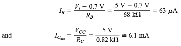
If we test the the equation 2 with these results we get:
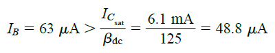
This appears to be perfectly satisfying the required condition. No doubt, any value of IB which is higher than 60 uA will be allowed to enter across Q-point over the load line situated extremely closely to the vertical axis.
Now, referring to the BJT network shown in the first diagram, while Vi = 0 V, IB = 0 uA, and asuming IC = ICEO = 0 mA, the voltage drop occurring across RC will be as per the formula:
VRC = ICRC = 0 V.
This gives us VC = +5 V for the first diagram above.
In addition to computer logic switching applications, this BJT configuration can be also implemented like a switch using the same extreme points of the load line.
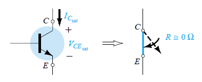
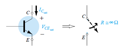
When saturation takes place, the current IC tends to get quite high, which corresponding drops the voltage VCE to a lowest point.
This gives rise to a resistance level across the two terminals as depicted in the following figure and calculated using the following formula:
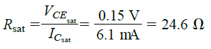
R(sat) = VCE(sat) / IC(sat) as indicated in the following figure.
If we assume a typical average value for the VCE(sat) such as 0.15 V in the above formula, we get:
This resistance value across the collector emitter terminals looks quite small when compared to a series resistance in kilo Ohms at the collector terminals of the BJT.
Now, when the input Vi = 0 V, the BJT switching will be cut off causing the resistance across the collector emitter to be:
R(cutoff) = Vcc / ICEO = 5 V / 0 mA = ∞ Ω
This gives rise to an open circuit kind of situation across the collector emitter terminals. If we consider a typical value 10 uA for the ICEO, the value of the cut off resistance will be as given below:
Rcutoff = Vcc / ICEO = 5 V / 10 uA = 500 k Ω
This value looks significantly large and an equivalent to an open circuit for most BJT configuration as a switch.
Solving a Practical Example
Calculate the values of RB and RC for a transistor switch configured like an inverter below, given that ICmax = 10mA
The formula for expressing collector saturation is:
ICsat = Vcc / Rc
∴ 10 mA = 10 V / Rc
∴ Rc = 10 V / 10 mA = 1 kΩ
Also, at saturation point
IB ≅ IC(sat) / βdc = 10 mA / 250 = 40 μA
For guaranteed saturation let's select IB = 60 μA, and by using the formula
IB = Vi - 0.7 V / RB, we get
RB = 10 V - 0.7 V / 60 μA = 155 kΩ ,
Rounding off the above result to 150 kΩ, and evaluating the above formula again we get:
IB = Vi - 0.7 V / RB
= 10 V - 0.7 V / 150 kΩ = 62 μA,
since IB = 62 μA > ICsat / βdc = 40 μA
This confirms the we have to use RB = 150 kΩ
Calculating Switching Transistors
You will find special transistors called switching transistors due to their fast rate of switching from one voltage level to another.
The following Figure compares the time periods symbolized as ts, td, tr, and tf with the collector current of the device.
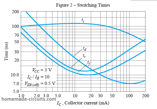
The effect of the time periods on the collector speed response is defined by the collector current response as shown below:
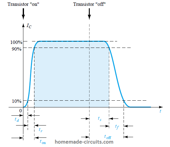
The total time needed for the transistor to switch from the “off” to the “on” state is symbolized as t(on) and can be established by the formula:
t(on) = tr + td
Here td identifies the delay happening while the input switching signal is changing state and the transistor output is responding to the change. The time tr indicates the final switching delay from 10% to 90%.
The total time taken by a bJt from a turned ON state to turned OFF state is indicated as t(off), and expressed by the formula:
t(off) = ts + tf
ts determines the storage time, while tf identifies the fall time from 90% to 10% of the original value.
Referring to the above graph, for a general purpose BJT, if the collector current Ic = 10 mA, we can see that:
ts = 120 ns, td = 25 ns, tr = 13 ns, tf = 12 ns
which means t(on) = tr + td = 13 ns + 25 ns = 38 ns
t(off) = ts + tf = 120 ns + 12 ns = 132 ns


Comments (15)
Hi Swagatam, hope you are well.
I’ve been trying to get my head around calculating the base resistor value for a given load but I just can’t get it to sink in or get results that make sense…even after reading your tutorial above. I’m probably missing something really obvious but don’t know where I’m going wrong.
I’m going to build an LED chaser based on your “Knight Rider” circuit but use 2 banks of 6 LED’s at each output to make a wide bar. Would you kindly look over my “test” schematic and tell me if the values quoted are correct and how to work out the base resistor (R1 in the circuit) from those values?
You’ll find the schematic here: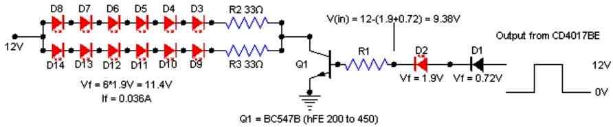
Many thanks
Steve
Hi Steve,
The formula is very simple actually:
R1 = (Supply Voltage at Transistor base – 0.7) x hFE / Total LED Current
Thanks for taking a look…much appreciated; thought I was missing something really simple. For the circuit attached, that formula gives me a value of 48.2k ohms using hFE=200…sounds very high?
Yes, it looks high but is is correct.
Nevertheless the value is not critical at all. You an simply use a 10K resistor without any issues or worries.
If I use a BC547A (hFE=110), a 10k resistor would limit collector current to about 95mA; which is far more than what I need but still within the parameters of the transistor. But I will be using a BC547B, as it’s the only one I can get locally, which has hFE=200. Would a 10k base resistor potentially allow more collector current than the transistor can supply; assuming a 12V supply rail?
Your LEDs have series resistors so the current can never increase above 40 mA for both the strings combined. So it is absolutely fine.
Thank you so much for explaining; it is clear to me now.
You are welcome!
Hi ,
I am using transistor(Two) ckt as level shifting of UART , Could you please help to calculate first transistor and second transistor collector output voltage ?
Hi, can you please show me the link of the schematic. Without seeing it I cannot suggest a solution.
Hi, Sorry for this dumb question.
Can we build transistor as a switch with common base / common collector configuration?
Thanks.
Hi, yes transistors are used as switches in DC circuits
Can you show me what the circuit looks like?
I’ve been searching on google, but I can’t find the circuit that use common base/collector configuration.
There are some good videos on youtube which you can watch and understand them thoroughly…
I would like to learn designing practical electronic circuits using PCBs. I want to start making Arc Welding Machines, Battery chargers and many more just to mention a few. I am not an Engineer but I have a Hamble knowledge of Electronics in general and I would like to improve that knowledge by interacting with High Powered Engineers like you. I will be sending you some requests and questions from time to time in this regard.
Kind regards,
Victor.