In this post I will comprehensively explain how to protect mosfets and prevent mosfet burning in electronic circuits by following some basic guidelines related to correct PCB layout, and careful manual handling of these sensitive devices.
Introduction
Even after connecting everything correctly you find the mosfets in your circuit becoming HOT and blowing off within minutes. This is quite a common issue faced by most new as well as experienced hobbyists while designing and optimizing mosfet based circuits especially the ones which involve high frequencies.
Obviously, connecting all the parts correctly as per the given details is the main thing that needs to be checked and confirmed first before assuming other issues, because unless the fundamental things are put absolutely right it would be meaningless tracing the other hidden bugs in your circuit.
Basic Mosfet protection application becomes critical specifically in those circuits which involve high frequencies in the order of many kHz. This is because high frequency applications calls for quick (within ns) turn ON and OFF of the devices which in turn demands efficient implementation of all the criteria associated directly or indirectly with the concerned switching.
So what are the main hindrances which cause improper or inefficient switching of the mosfets, I have explained comprehensively how to protect mosfets with the following points.
Get Rid of Stray Inductance:
The most common and prime bug in the que is the stray inductance that may be hidden within the circuit tracks. When the switching frequency and current are high, even a slightest unnecessary increase in the connecting path that is the PCB track may result in inter-linked inductance which in turn may affect the mosfet behavior drastically due to inefficient conduction, transients and spikes.
In order to get rid of this issue it's strongly recommended to keep the tracks wider and to keep the devices AS CLOSE AS POSSIBLE to each other and to the driver IC which are being used to drive the respective mosfets.
That's why SMD is preferred and is the best way of eliminating cross inductance across the components, also the use of double sided PCB helps controlling the issue due to its short "printed-through-hole" connections across the components.
Even the standing height of the mosfets must be brought to minimum by inserting the lead as deep down as possible into the PCB, using SMD is probably the best option.
We all know that mosfets include in-built capacitors which require charging and discharging in order to make the device conduct.
Basically these capacitors are connected across the gate/source and gate/drain. Mosfets "don't like" prolonged delayed charging and discharging of its capacitance since these are directly related to its efficiency.
Connecting the mosfets directly to a logic source output might seem to solve this problem, because the logic source would easily switch and sink the capacitance from Vcc to zero quickly, and vice versa due to the absence of any obstacle in its path.
However, implementing the above consideration could also lead to the generation of transients and negative spikes with dangerous amplitudes across the drain and gate making the mosfet vulnerable to the generated spikes due to sudden high current switching across drain/source.
This could easily break the silicon separation between the sections of the mosfet rendering a short circuit inside the device, and damaging it permanently.
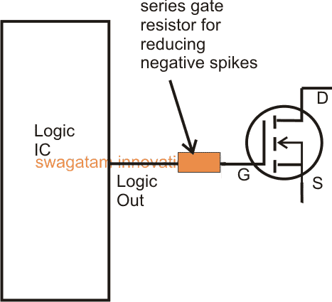
Importance of Gate Resistance:
To get rid of the above issue it is recommended to use low value resistor in series with the logic input and the mosfet gate.
With relatively lower frequencies(50 Hz to 1kHz), the value could be anywhere between 100 and 470 ohms, while for frequencies above this the value could be within 100 ohms, for much higher frequencies (10kHz and above) this must not exceed 50 ohms.
The above consideration allows exponential charging or gradual charging of the internal capacitors reducing or blunting of the chances of negative spikes across the drain/gate pins.
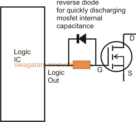
Using Reverse Diodes:
In the above consideration an exponential charging of the gate capacitance reduces the chances of spikes but that also means that the discharging of the involved capacitance would be delayed due to the resistance in the path of the logic input, every time it switches to logic zero. Causing a delayed discharging would mean forcing the mosfet to conduct under stressful conditions, making it unnecessarily warmer.
Including a reverse diode parallel with the gate resistor is always a good practice, and simply tackles the delayed discharging of the gate by providing a continuous path for the gate discharge through the diode and into the logic input.
The above mentioned points regarding correct implementation of mosfets can be easily included in any circuit in order to safeguard mosfets from mysterious malfunctions and burning.
Even in complicated applications such half-bridge or full bridge mosfet driver circuits along with some additional recommended protections.
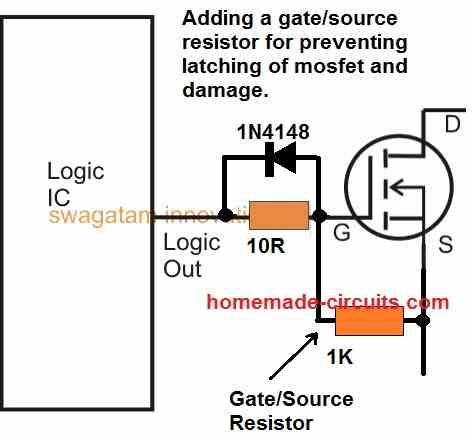
Using a Resistor Between Gate and Source
Although we have not indicated this inclusion in the previous images, this is strongly recommended to safeguard the mosfet from blowing of under all circumstances.
So how does a resistor across gate/source provide a guaranteed protection?
Well, normally mosfets have the tendency to latch up whenever a switching voltage is applied, this latching effect can sometimes be hard to revert, and by the time an opposite switching current is applied it is already too late.
The mentioned resistor ensures that as soon as the switching signal is removed the mosfet is able to quickly turn OFF, and prevent a possible damage.
This resistor value could be anywhere between 1K and 10K, however lower values would provide better and more effective results.
Avalanche Protection
MOSFETs may get damaged if its junction temperature suddenly increases beyond the tolerable limit due to over voltage conditions across its internal body diodes. This occurrence is termed as avalanche in MOSFETs.
The problem can arise when an inductive load is used at the drain side of the device, and during the MOSFET switch OFF periods the inductor's reverse EMF passing through the MOSFET body diode becomes too high, causing a sudden rise in the MOSFET's junction temperatures, and its breakdown.
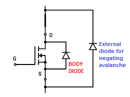
The problem can be tackled by adding an external high power diode across drain/source terminals of the MOSFETs, so that the reverse current is shared across the diodes, and excess heat generation is eliminated.
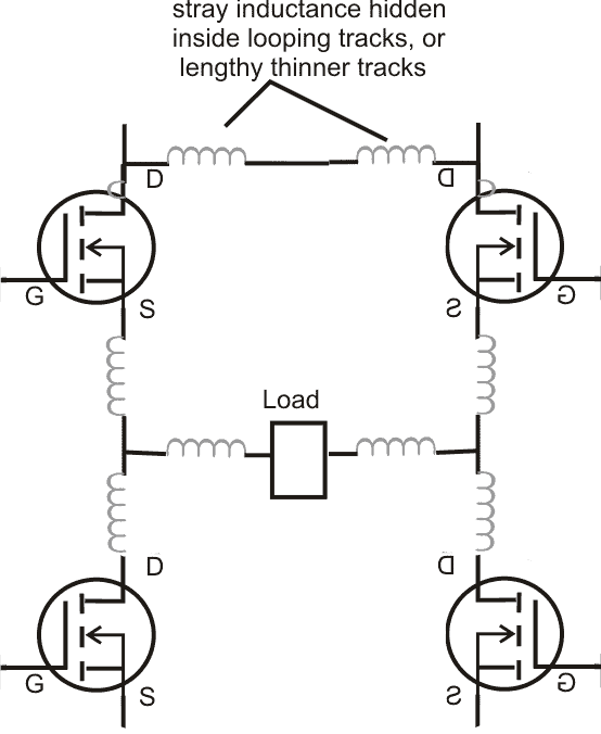
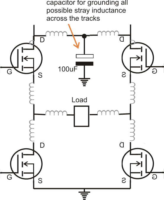
Protecting Mosfets in H-Bridge Circuits from Burning
While using a full bridge driver circuit involving a driver IC such as the IR2110 in addition to the above, the following aspects should be bored in mind (I'll discuss this in details in one of my upcoming articles soon)
- Add a decoupling capacitor close to the driver IC supply pinouts, this will reduce the switching transients across the internal supply pinouts which in turn will prevent unnatural output logic to the mosfet gates.
- Always use high quality low ESD, low leakage type of capacitors for the bootstrapping capacitor and possibly use a couple of them in parallel. Use within the recommended value given in the datasheet.
- Always connect the four mosfet interlinks as close as possible to each other. As explained above this will reduce stray inductance across the mosfets.
- AND, connect a relatively large value capacitor across the high side positive (VDD), and the low side ground (VSS), this will effectively ground all stray inductance that may be hiding around the connections.
- Join the VSS, the mosfet low side ground, and the logic input ground all together, and terminate into a single common thick ground to the supply terminal.
- Last but not the least wash the board thoroughly with acetone or similar anti-flux agent in order to remove all possible traces of the soldering flux for evading hidden inter connections and shorts.
Protecting Mosfets from OverHeating
Lighting dimmers often suffer from MOSFET failures. Most dimmers used in low-temperature AC industrial applications are enclosed and often embedded in the wall. This can cause heat dissipation issues, and can result in heat build-up - leading to a thermal event. Usually, the MOSFET used for the lighting dimmer circuits fails in 'resistive mode'.
A reflow-able thermal protection or RTP from TE Connectivity provides an answer to MOSFET failure in low-temperature AC applications.
This device acts like a low-value resistor at the normal operating temperatures of the MOSFET. It is mounted almost directly on the MOSFET, and is therefore able to sense the temperature with precision. If for any reason, the MOSFET drifts into a high temperature condition, this is sensed by the RTP, and at a predefined temperature, the RTP changes into a high-value resistor.
This effectively cuts off the power to the MOSFET, saving it from destruction. Thus, a lower priced resistor sacrifices itself to save a more expensive MOSFET. A similar analogy could be the use of a fuse (low-value material) in protecting more complex circuitry (e.g. a television).
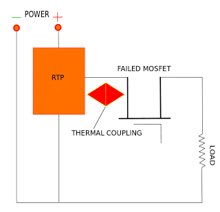
One of the most interesting aspects of the RTP from TE Connectivity is its ability to withstand enormous temperatures - up to 260ºC. This is surprising since the resistance change (to protect the MOSFET) usually occurs at around 140ºC.
This miraculous feat is accomplished via innovative design by TE Connectivity. The RTP has to be activated before it starts protecting the MOSFET. The electronic activation of the RTP occurs after the flow soldering (attachment) is completed. Each RTP has to be individually armed by sending a specified current through the arming pin of the RTP for a specified time.
The time-current characteristics are part of the specifications of the RTP. Before it is armed, the value of the resistor of the RTP will follow the specified characteristics. However, once it is armed, the arming pin will become electrically open - preventing further changes.
It is very important that the layout specified by TE Connectivity be followed when designing and mounting the MOSFET and the RTP on the PCB. Since the RTP has to sense the temperature of the MOSFET, it naturally follows that the two should remain in close proximity.
The RTP resistance will allow up to 80A of current at 120V AC through the MOSFET as long as the temperature of the MOSFET remains below the Open Temperature of the RTP, which can be between 135-145ºC.


Comments
Hie. I am making an inverter with an ir 2110 and irf1310n mosfets. My driver and mosfets keep on burning, pliz help. My transformer is centre tapped.
Connect a incandescent bulb in series with the supply, if the bulb remains switched ON without a load connected at the full bridge output that would mean either your bridge is configured wrongly, or the MOSFETs are bad, or the IC is not oscillating.
Sir swagatam,can the latching resistor be important to the mosfets mostly when the mosfets are receiving stepped down ac from the transformer in order to charge the batteries? I had tried this with an inverter with a centre tap transformer and found it working. The only thing I did was to improvise a change over system for isolation of the oscillator during the presence of mains power and to connect back to inverter mode when mains go off by the use of a 12v /1A transformer connected to the mains grid for powering the relays. Iam yet to try with this full bridge system,do you have anything in mind you can share with me?
Evans, without seeing the schematic it can be difficult to answer your question, but anyway MOSFETs are not designed to handle AC, and will blow if an AC is used to drive it.
Hello sir swagatam,av send you the diagram,look at it and see if it is possible
Evans, I checked the diagram, it seems the battery is being charged through the MOSFET’s body diode. When the gate pulse is removed the gate/source 1K switches off the MOSFET, which blocks the negative cycles from the AC, and allows only the positive through the MOSFET body diode which charges the battery.
You are right sir swagatam, that’s what was talking about,now can we employ the same principle to the h bridge system? Share with me any sketch you might have in mind,thank you.
Ok sir,let me do some research and if I succeed,will share with you. Thanks for your time.
No problem Evans, wish you all the best!
Ok sir swagatam,but do you think what am thinking? That in an instance am using relays then they should be able to switch at the same time without delay to avoid Short circuit. Or we should create some delay for the oscillator such that the boostraping network is switched on first ,then some delay like 5sec then the oscillator comes on? But this now delay might be a problem since some machines like CPUs might loose data in the process coz they will go off for the period 5sec delay is in place. Anything you can advise?
You are correct Evans, the N channel MOSFETs must be switched OFF before the AC is reverted to the MOSFETs, and if appropriate delays are included the inverter cannot be used like an UPS
Ok sir swagatam,got you but what about in a situation am using a boostraping network instead of specialized ics? What happens to the diode IN4148 that is connected to the positive terminal of the battery? I think during charge time ,some voltage will be still passing to charge the capacitor hence gates of the mosfets on the higher side might misbehave,and this might be recipe for trouble. Also look at the connection of 10uf/50v capacitor,will the stepped down ac from transformer not have some impact? Help solve this dilemma.
For a discretely bootstrapped full bridge stage it can be a problem, because the 4 N channel MoSFET cannot be disabled with a single direct supply input. There’s no way except using a relay to cut off the positive battery from the diode/capacitor and the ICs stages.
Evans, in that case you only have to activate the SD pin of the IC IRS2453(1)D. To do this connect the SD pin of the IC to ground through a 10K resistor, and apply a +12V DC link from a grid based 12 V adapter. Once this is done, the grid mains will need to be changedover to the transformer secondary winding, this will automatically allow the 4 MOSFETs to pass the stepped down AC from the transformer through the MOSfeT body diodes in to the battrey.
Also make sure to add 1K resistors across gate/source of all the mosfets
Hello Swagatam:
I need to develop a Push-pull H-Bridge converter 200W 100KHZ system. The system needs to be very efficient.
Do you please develop a system against Consultancy Fees Basis.
Kindly help.
Hello Kuldeep,
you can try the second design from this article:
https://www.homemade-circuits.com/simplest-full-bridge-inverter-circuit/
You can consult me through comments under the same article, I’ll guide you through until finish, free of cost.
I have repaired a dc drive having 2 mosfets/igbts…..D4068 configured in parallel driven by PWM for 180volt treadmill motor. Very close to the heat sink of mosfets, I have seen a hard copper wire shaped as pwm-on-state figure soldered on the pcb, marked as RT. Can you explain me to get learning as to what purpose it serve….? Thanks a lot, to whom it may concern, with all due regards.
Sorry could not understand what you meant by “..shaped as pwm-on-state figure soldered on the pcb…” please clarify this, I’ll try to figure out.
Hi,
I’m designing a Battery management system for my Li ion battery pack and I have used np pair mosfets for discharging across resistor(how can I upload and show my schematic)and differential opamps to monitor the battery voltages. the circuit works fine but there are some fluctuations when I turn on the mosfets. I want to know where can I have to put these Capacitor to eliminate this noise and why are they fluctuating.
Hi, you can upload the image on any free image hosting site or in dropbox . com and send me the link here, I will try to solve it!
Hello swagatam, I have built an inveterate using sg3524. The inverter works very well during operation. But anytime I try to turn on the inverter when the battery is fully charged, the mosfet fails. When the battery is not very fully charged, it starts up well, but even with that I see the transformer make a sudden heavy hum when I turn on the inverter. It looks like the inverter draws a lot if sudden current when it is initially turned on.but after it is able to turn on successfully it works very well…so my problem now has to do with mosfet failing during inverter startup…I really need your help
Hello carter,
SG3524 IC includes a slow start feature which you can effectively employ for tackling this issue.
This may be executed by connecting a 100uF/25V capacitor from positive line to pin#10, and also by keeping a 10K resistor connected from pin#10 to the ground line.
the above precautions are specific for high frequency circuits, for 50Hz inverter this might not be so critical…
Please sir, is it possible to design a simple circuit that can charge your cellphone battery with 4×1.5v duracell battery pack for 1 year use?
Hi J-boy,
Would it be possible for any human to survive for a year with a months ration in hand, same applies to your question….
Hi Michael,
Due to the present work load I am finding it hard to concentrate on all the fields, kindly bear with me, I'll try to get back as soon as possible.