The following inverter designs are unique modified sine wave inverter concepts designed me. The entire unit along with the oscillator stage and the output stage can be easily built by any electronic enthusiast at home. The present designed will be easily able to support 500 VA of output load.
Let's try to understand the circuit functioning in details:
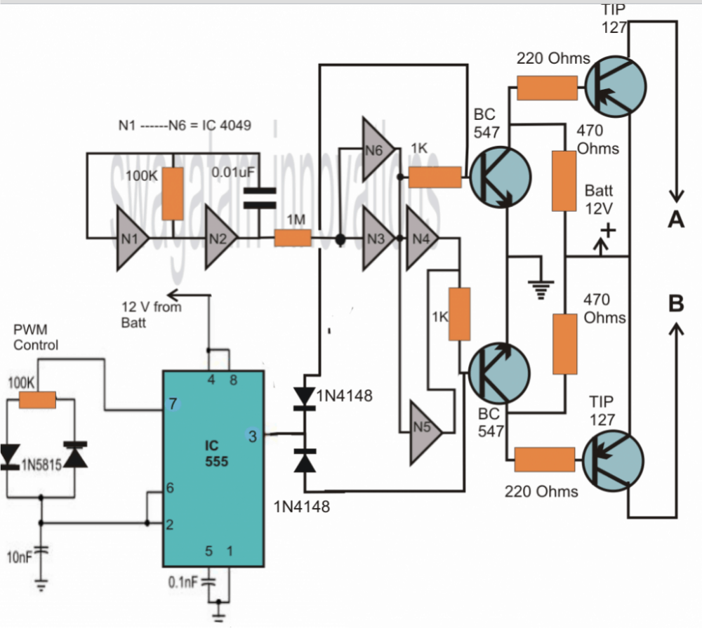
The Oscillator Stage:
Looking at the circuit diagram above, we see a clever circuit design comprising both, the oscillator as well as the PWM optimization feature included.
Here, the gates N1 and N2 are wired up as an oscillator, which primarily generates perfectly uniform square wave pulses at its output. The frequency is set by adjusting values of the associated 100K and the 0.01 uF capacitor. In this design it is fixed at the rate of around 50 Hz. The values can be altered appropriately for getting a 60 Hz output.
The output from the oscillator is fed to the buffer stage consisting of four parallel and alternately arranged NOT gates. The buffers are used for sustaining perfect pulses and for avoiding degradation.
The output from the buffer is applied to the driver stages, where the two high-power darlington transistors take the responsibility of amplifying the received pulses, so that it can be finally fed to the output stage of this 500 VA inverter design.
Until this point the frequency is just an ordinary square wave. However the introduction of the IC 555 stage entirely changes the scenario.
The IC 555 and its associated components are configured as a simple PWM generator. The mark-space ratio of the PWM can be discretely adjusted with the help of the pot 100K.
The PWM output is integrated to the output of the oscillator stage via a diode. This arrangement makes sure that the generated square wave pulses are broken into pieces or chopped as per the setting of the PWM pulses.
This helps in reducing the total RMS value of the square wave pulses and optimize them as close as possible to a sine wave RMS value.
The pulses generated at the bases of the driver transistors are thus perfectly modified to resemble sine wave forms technically.
The Output Stage:
The output stage is quite straight forward in its design. The two winding of the transformer are configured to the two individual channels, consisting of banks of power transistors.
The power transistors at both the limbs are arranged in parallel to increase the overall current through the winding so as to produce the desired 500 watts of power.
However to restrict thermal runaway situations with the parallel connections, the transistors are connected with a low value, high wattage wire wound resistor at their emitters. This inhibits any single transistor from getting over loaded and fall into the above situation.
The bases of the assembly are integrated to the driver stage discussed in the previous section.
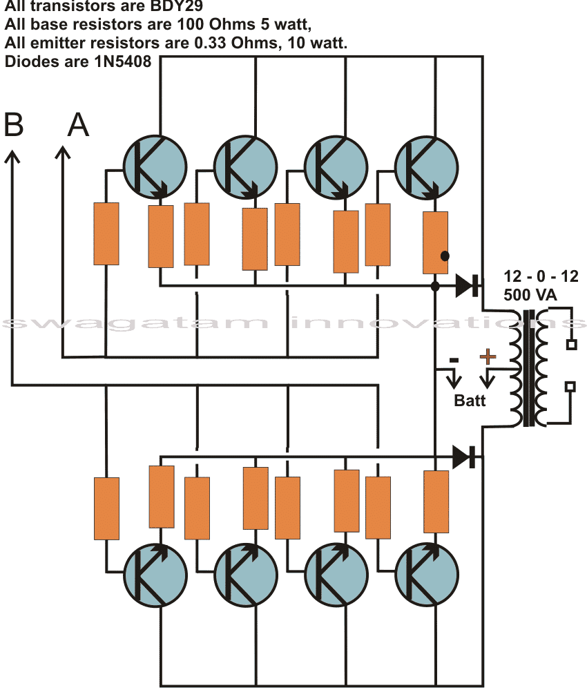
The battery is connected across the center tap and the ground of the transformer and also to the relevant points in the circuit.
Switching ON power immediately starts the inverter, providing rich modified sine wave AC at its output, ready to be used with any load upto 500 VA.
The component details are supplied in the diagram itself.
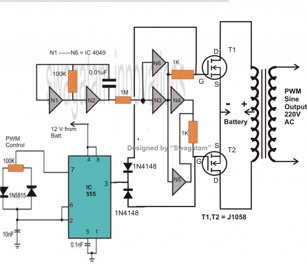
The above design can also be modified into a 500 watt PWM controlled mosfet sine wave inverter by replacing the driver transistors simply by a few mosfets. The design shown below would provide about 150 watts of power, for obtaining 500 watts, more number of mosfets may be required to be connected in parallel with the existing two mosfets.
Using a 4093 IC for the Modified Results
The PWM controlled modified sine wave inverter circuit presented below is our 3rd contender, it uses just a single 4093 for the specified functions.
The IC consists of four NAND gates, out of which two are wired up as oscillators while the remaining two as buffers.
The oscillators are integrated in such a way that the high frequency from one of the oscillators interacts with the output of the other, generating chopped square waves whose RMS value can be well optimized to match the regular sine waveforms.Inverter designs are not always easy to understand or build, especially so when it's as complex as modified sine wave types. However the concept discussed here utilizes just a single IC 4093 for handling all the required complications. I have explained how simple it is to build.
Parts you will Ned to Build this 200 Watt Inverter Circuit
All Resistors are 1/4 watt, 5 %, unless otherwise specified.
- R1 = 1 M for 50 Hz and 830 K for 60 Hz
- R2 = 1 K,
- R3 = 1 M,
- R4 = 1 K,
- R5, R8, R9 = 470 Ohms,
- R6, R7 = 100 Ohms, 5 Watt,
- VR 1 = 100 K,
- C1, C2 = 0.022 uF, Ceramic Disc,
- C3 = 0.1, disc ceramic
- T1, T4 = TIP 122
- T3, T2 = BDY 29,
- N1, N2, N3, N4 = IC 4093,
- D1, D1, D4, D5 = 1N4007,
- D3, D2 = 1N5408,
- Transformer = 12 -0 – 12 volts, current from 2 to 20 Amps as desired, output voltage can be 120 or 230 volts as per country specifications.
- Battery = 12 volts, typically a 32 AH type, as used in cars is recommended.
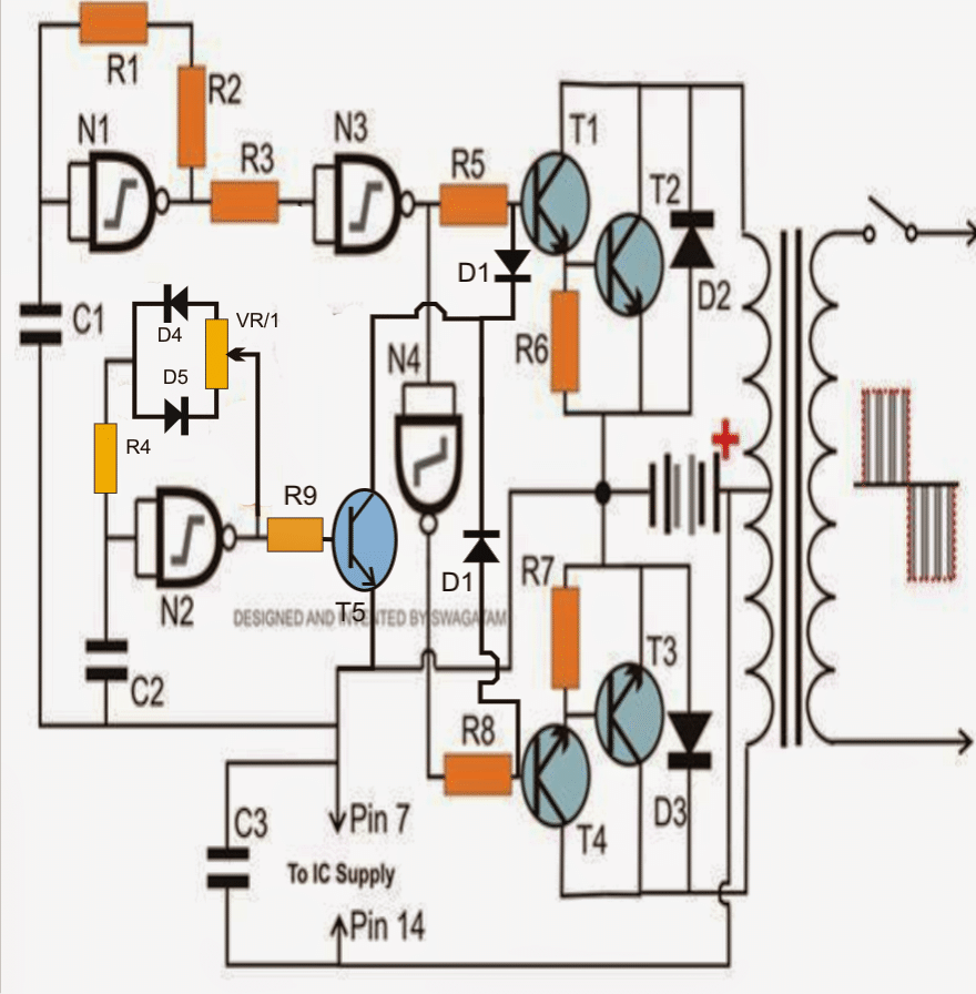
Circuit Operation
The proposed design of a 200 watt modified sine wave inverter obtains its modified output by discretely “cutting” the basic square wave pulses into smaller sections of rectangular pulses. The function resembles to a PWM control, commonly associated with IC 555.
However, here the duty cycles cannot be varied separately and is kept equal throughout the available variation range. The limitation does not affect the PWM function by much, since here we are only concerned in keeping the RMS value of the output close to its sine wave counter, which is executed satisfactory through the existing configuration.
Referring to the circuit diagram, we can see that the entire electronics hovers around a single active part – the IC 4093.
It consists of four individual NAND Schmitt gates, all of them have been engaged for the required functions.
N1 along with R1, R2 and C1 forms a classic CMOS Schmitt trgger type of oscillator where the gate is typically configured as an inverter or a NOT gate.
The pulses generated from this oscillator stage are square waves which forms the basic driving pulses of the circuit. N3 and N4 are wired up as buffers and are used for driving the output devices in tandem.
However these are ordinary square wave pulses and do not constitute the modified version of the system.
We can easily use the above pulses solely for driving our inverter, but the result would be an ordinary square wave inverter, not suitable for operating sophisticated electronic gadgets.
The reason behind this is that, square waves may differ greatly from the sine waveforms, especially as far as their RMS values are concerned.
Therefore, the idea is to modify the generated square waveforms so that its RMS value closely matches with a sine waveform. To do this we need to dimension the individual square waveforms through some external intervention.
The section comprising N2, along with the other associated parts C2, R4 and VR1, forms another similar oscillator like N1. However this oscillator produces higher frequencies which are tall rectangular shaped.
The rectangular output from N2 is fed to the basic input source of N3. The positive trains of pulses have no effect on the source input pulses due to the presence of D1 which blocks the positive outputs from N2.
However, the negative pulses are allowed by D1 and these effectively sink the relevant sections of the basic source frequency, creating kind of rectangular notches in them at regular intervals depending upon the frequency of the oscillator set by VR1.
These notches or rather the rectangular pulses from N2 can be optimized as desired by adjusting VR1.
The above operation cuts the basic square wave from N1 into discrete narrow sections, lowering the average RMS of the waveforms. It is advised that the setting is done with the help of a RMS meter.
The output devices switch the relevant transformer windings in response to these dimensioned pulses and produce corresponding high voltage switched waveforms at the output winding.
The result is a voltage which is quite equivalent to a sine wave quality and is safe for operating all types of household electrical equipment.
The inverter power may be increased from 200 watts to 500 watts or as desired simply by adding more numbers of T1, T2, R5, R6 and T3, T4, R7, R8 in parallel over the relevant points.
Salient Features of the Inverter
The circuit is truly efficient and moreover it is a modified sine wave version which makes it outstanding in its own respect.
The circuit utilizes very ordinary, easy to procure types of components and is also very cheap to build.
The modifying process of the square waves into sine waves can be done by varying a single potentiometer or rather a preset, which makes the operations pretty simple.
The concept is very basic yet offers high power outputs which may be optimized as per ones own needs just by adding a few more number of output devices in parallel and by replacing the battery and the transformer with the relevant sizes.


Need Help? Please Leave a Comment! We value your input—Kindly keep it relevant to the above topic!