Although a variety of laboratory power supplies have appeared in recent times, only handful of these will provide you with the efficiency, versatility, and low cost of the design detailed in this article.
In this article I have explained a highly regulated, DIY, laboratory grade power supply with dual 0-50 volt. The voltage and current ranges are independently variable from 0 to 50 V, and 0 to 5 amps respectively..
Having said that, because of the DIY layout, you can customize the settings as needed, which can witnessed in the following specification table..
- Number of Supplies = 2 (Fully Floating)
- Voltage Range = 0 to 50V
- Current Range = 0 to 5 amps
- Coarse control and Fine Control ratio for both current and voltage = 1:10
- Voltage Regulation = 0.01% line, and 0.1% load
- Current Limiter = 0.5%
You Will Also Like: How to Design a Bench Power Supply Circuit
Circuit description
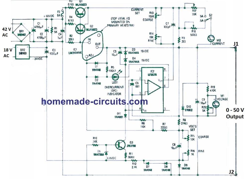
Figure 1 above shows the circuit diagram of the laboratory power supply. The specifications of the layout is centered around IC1, an LM317HVK adjustable regulator, for wide-ranging functionality. The "HVK" suffix suggests the high-voltage edition of the regulator.
The remaining portion of the circuit enables voltage setting and current limiting capabilities. The input to IC1 originates from the output of BR1, which is filtered by C1 and C2 to around + 60 volts DC, and the input for current-sense comparator IC2 develops from bridge rectifier BR2, which furthermore works like a negative bias supply to get regulation to ground level.
The function of IC1 is to keep the OUT terminal at 1.25 volts DC over the ADJ terminal. The current drain at the ADJ pin is extremely minimal (as low as 25 µA) and, therefore, R15 and R16 (the crude and refined voltage manipulations) and R8 form a voltage divider, with 1.25 volts showing up around R8.
The lower terminal of R16 attaches to a -1.3 reference volt developed by D7 and D8, permitting the R8 - R15 resistive divider fix the output voltage right down to ground level any time R15 + R16 becomes 0 ohms.
Calculating the Output Voltage
Generally speaking, the output voltage depends upon, the following results:
(VouT - 1.25 + 1.3) / (R15 + R16) = 1.25 / R8.
Thus, the highest magnitude of voltage value available from each variable supply board can be:
VOUT= (1.25 / R8) x (R15 + R16) = 50.18 volts DC.
Potentiometers R15 and R16 is used for controlling the output voltage, which enables the VouT to vary from 0-50 volts DC.
How Current Control Works
When the DC load current increases, the voltage drop across R2 also rises, and at around 0.65 volts (that is relative to around 20 mA), Q1 and Q2 switch on, becoming the primary course of the current. Additionally, R3 and R4 guarantee that Q1 and Q2 handle the load uniformly. IC2 works like a Current limiter stage.
Its non-inverting input makes use of the output voltage like a reference, while its inverting input is attached to the voltage divider developed by R6 and the current control pots R13 and R14. The voltage drop across R6 is about 1.25 volts, the reference voltage stated above is determined by the difference across the IC1 terminals OUT and ADJ.
Current passing across Q1 and Q2 moves via R9, building a voltage drop across R13 + R14. As a result, IC2 is forced to switched OFF as soon as the voltage drop around R9 generates current by means of R13 and R14, causing the non-inverting input voltage to go beyond VouT.
This fixes the current limiting threshold at: (IouT x 0.2)/(R13 + R14) = 1.25/100K; low = 0 to 5 amps. This provides a corresponding a range of around 0-5 amps.
When the current limit threshold is reached, output of IC2 becomes low, driving the ADJ pin down by way of D2 and resulting in the illumination of LED1. Extra current for D5 is delivered by R5.
As the ADJ pin is driven low, the output follows, until the output current falls to a point equivalent to the setting of R13 and R14.
Considering that the output voltage could be between 0-50 volts, the supply voltage for IC2 should follow this range working with D3, D4, and Q3.
Then, D9 ascertains that the output voltage won't increase once the supply input is turned off, while D10 safeguards against a reverse supply voltage. Lastly, the meters M1 displays the voltage reading and M2 displays the current reading.
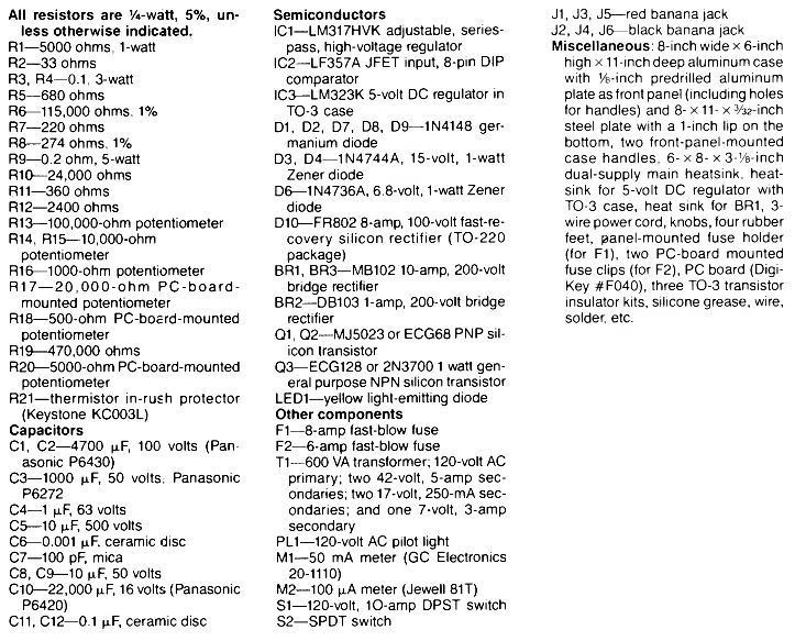
Parts List
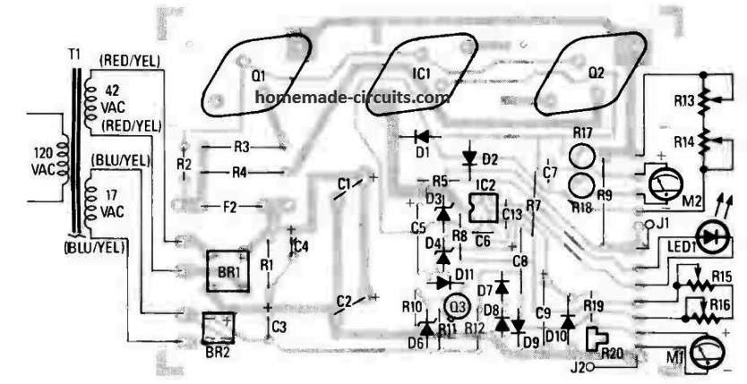
PCB Layout Design
Another Simple Laboratory Power Supply Circuit using LM324 IC
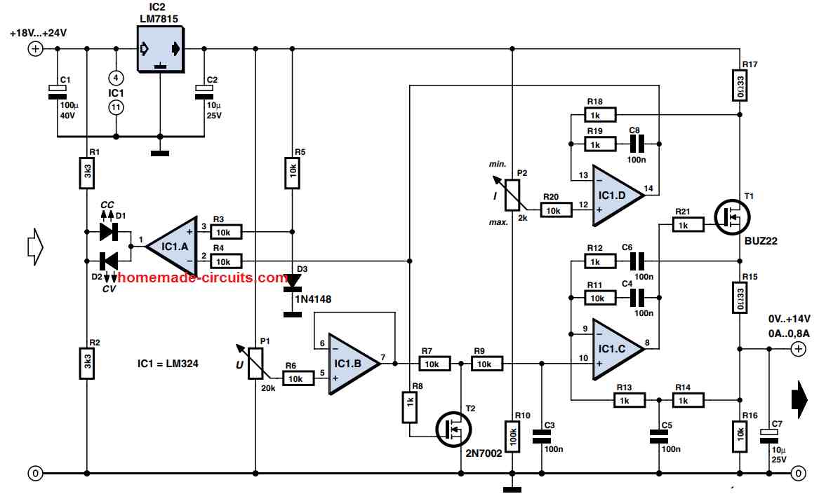
To obtain an intermediate supply voltage the regulator IC LM7815 has been used here. Its output travels by means of R17, that reads the output current, for th MOSFET T1.
This MOSFET is operated through the opamp IC1, configured like a voltage regulator. In this laboratory power supply circuit R11 and C4 establish the control loop's bandwidth, which enables the elimination of oscillation at increased frequencies.
Resistor R15 guarantees that capacitive loads having reduced effective resistance will not cause the control loop to become unstable. The AC content's negative feedback of the current through R12 and C5 enables the circuit to be perfectly reliable even while a large capacitor is employed at its output of the power supply.
The DC content's negative feedback through the low-pass filter is established by resistor R14 and capacitor C6. This configuration guarantees that the voltage drop developed across the resistor R15 is effectively compensated for.
The output capacitor C7 delivers a low impedance source for high-frequency loads. The resistor R16 helps the discharge of the capacitor C17 whenever the set voltage is decreased in the absence of an output load.
The IC1D section works like a current regulator. Once again in order to make sure the lab power supply works with perfect stability, the feedback loop's bandwidth is restrained by the resistor R19 and the capacitor C8.
In case the voltage drop developed across the resistor R17 becomes higher than the value as adjusted by the preset P2, the current limiting feature of the circuit kicks in and the transistor T2 is triggered ON.
This action subsequently cuts down the input voltage to the voltage regulation circuit stage until the specified amount of output current is arrived at. Resistors R7, R9 and capacitor C3 guarantee that proper regulation of current does not produce overshoots of the output voltage and also ensures that there's no generation of resonance effect whenever an inductive load is connected at the output.
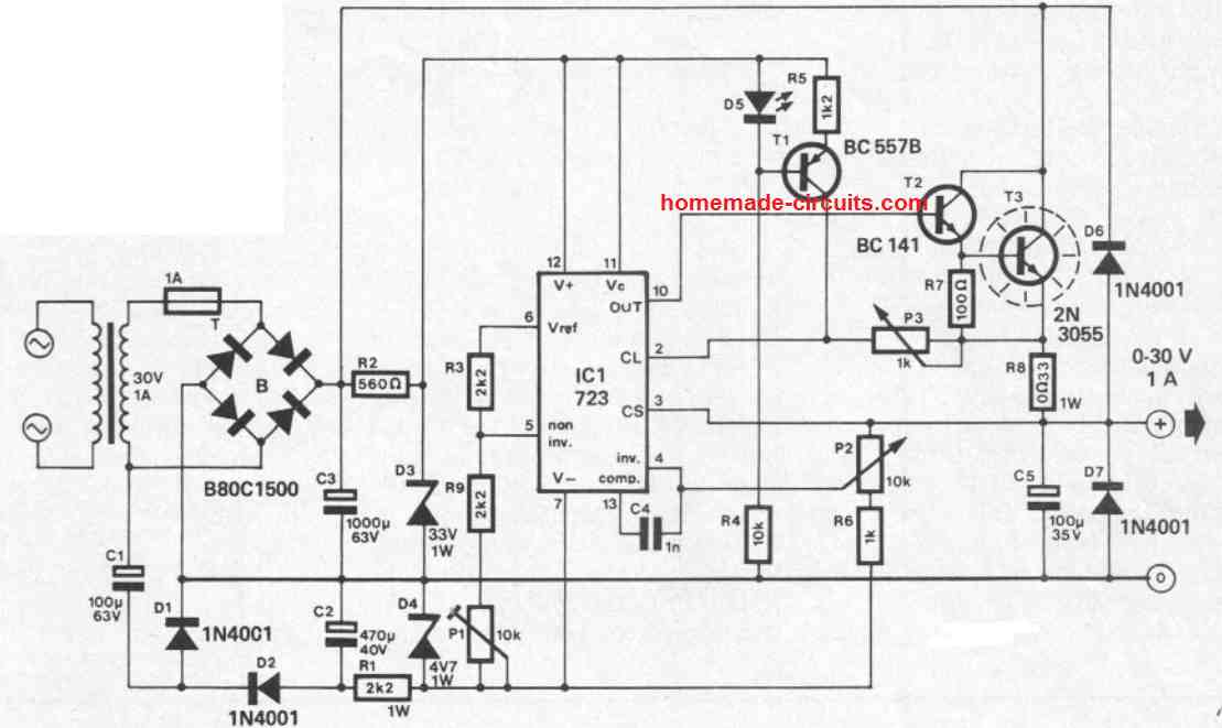
Using IC 723
The next design shows a simple yet extremely useful laboratory power supply using the IC LM723:


Comments
I need to make a 13.8 V, 25A power supply(adjustable) using this circuit , What are the changes I have to make? Please help
.