In this article I have explained using circuit diagrams how a clipper and a compressor circuits work to processes an input audio signal as per the required output signal.
What is an Audio Clipper
An audio clipper circuit is basically used to alter or restrict the amplitude (volume) of an audio signal. There are mostly two kinds of clippers:
Hard Clipper Circuit: A hard clipper circuit suddenly restricts the audio signal's loudness at a specific audio signal threshold level, . When the signal rises over this limit, it is "clipped" or flattened, producing distortion and an output that resembles a square wave.
Soft Clipper Circuit: Contrary to a hard clipper, a soft clipper progressively softens down the audio signal's peaks as it gets close to the threshold level. As a result, when the signal crosses the threshold, the distortion is smoother and more realistic.
In conclusion the audio signals with hard clippers have a harsh, abrupt distortion, whereas those with soft clippers have a smoother more subtle distortion.
Hard Soft Clipper Circuit
To compress the dynamic range of an audio signal, a gain-controlled or gain-limited stage is typically utilized, which is particularly effective in applications such as speech compression on PA systems and transmitters.
A gain-controlled stage is inherently more intricate compared to a gain-limited stage, often referred to as a clipper.
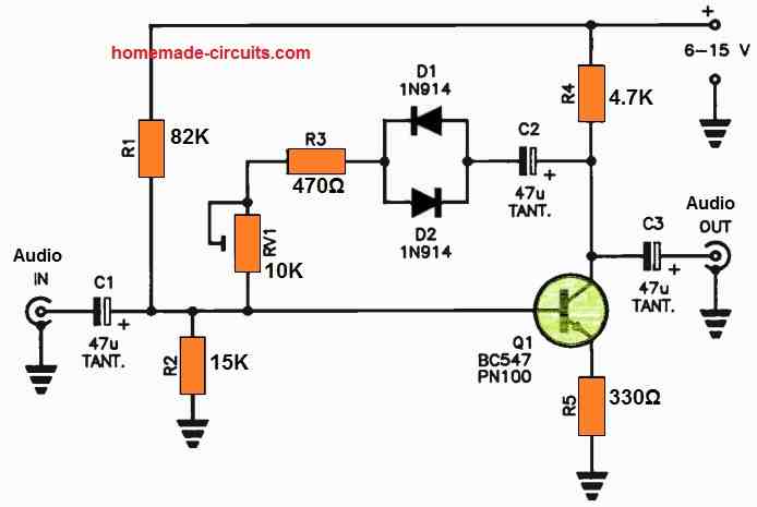
The simplest audio clipper circuit configuration as shown above involves the use of a pair of diodes arranged back-to-back, limiting the signal's voltage swing to approximately 0.6 V, resulting in a form of hard clipping where the input signal waveform is essentially truncated or clipped sharply at the peak.
This particular circuit employs a pair of back-to-back diodes within the feedback path of a single-stage transistor amplifier.
It incorporates a potentiometer control that may be used to vary the clipping characteristics, ranging from soft to hard.
When RV1 is set to its minimum value, it produces hard clipping, whereas at its maximum, it generates soft clipping.
It's worth noting that the stage's gain can be adjusted by altering the ratio of R4 to R5, with resistor R5 introducing a degree of degenerative feedback.
Following the stage, it is advisable to implement a low-pass filter to attenuate any harmonics produced during the clipping process.
Although tantalum capacitors are specified for use in this circuit, low-leakage alternatives can be substituted if needed. Any commonly available small-signal transistor can be employed for Q1.
This circuit should be integrated immediately after the microphone input stage.
Audio Clipper with Minimum Distortion
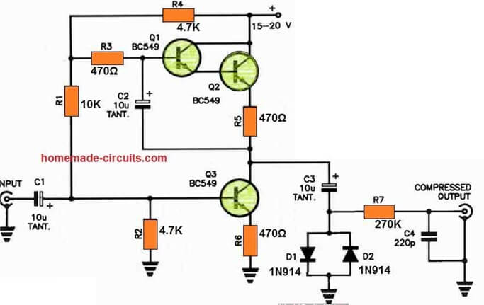
The issue commonly encountered with most audio signal clippers lies in their tendency to produce harsh harmonics due to the inherent asymmetry in many circuits.

This particular circuit addresses this problem by employing a pair of super-matched transistors, namely the LM394.
The LM394 features a unique construction where two transistors are intricately etched onto a single piece of silicon, ensuring an extremely close match in their characteristics.
Within this circuit, Q1 functions as the input stage and operates in a common-collector configuration, while Q2 serves as the output stage, operating in a common-base configuration.
This setup proves effective in achieving symmetrical clipping of the signal when overdriven at the input.
To establish proper biasing, R1 and R3 work together as a bias divider network, and R2 and R6 function as base isolation resistors. The circuit boasts a unity gain, and its input impedance is notably high.
What is an Audio Compressor
An audio compressor circuit is basically designed to minimize the dynamic range of an audio signal.
This is achieved by attenuating the amplitude of high audio peaks and boosting the quieter signal ranges.
This audio processing produces a more consistent and controlled output.
This helps to balance the audio output levels, causing the softer audio signals to become louder, and preventing distortions from extremely high audio peaks.
Compressor Circuit (Log)
Unlike clippers that compress the dynamic range of an audio signal once it surpasses a specific threshold, a compressor circuit with an input:output behavior closely resembling a logarithmic V [log.] curve delivers gradual signal limiting across an extensive range.
This results in a smoother compression effect.
This particular compressor circuit shown above exhibits a highly effective logarithmic input:output characteristic across a dynamic range spanning approximately 60 dB.
It achieves this through a pair of back-to-back diodes driven by a current generator, producing an almost ideal logarithmic transfer characteristic.
It's crucial to select diodes with closely matched forward resistance properties for optimal performance.
When it comes to polarized capacitors, you have the option of using either tantalum capacitors or low-leakage electrolytics.
Additionally, R7-C4 combination serves as a low-pass filter in this configuration. For optimal results, this stage should be inserted directly after the microphone amplifier.
An Alternative Logarithmic Compressor Design
This circuit shown below illustrates a method for achieving a logarithmic input:output characteristic in an amplifier stage, potentially serving as a compressor.
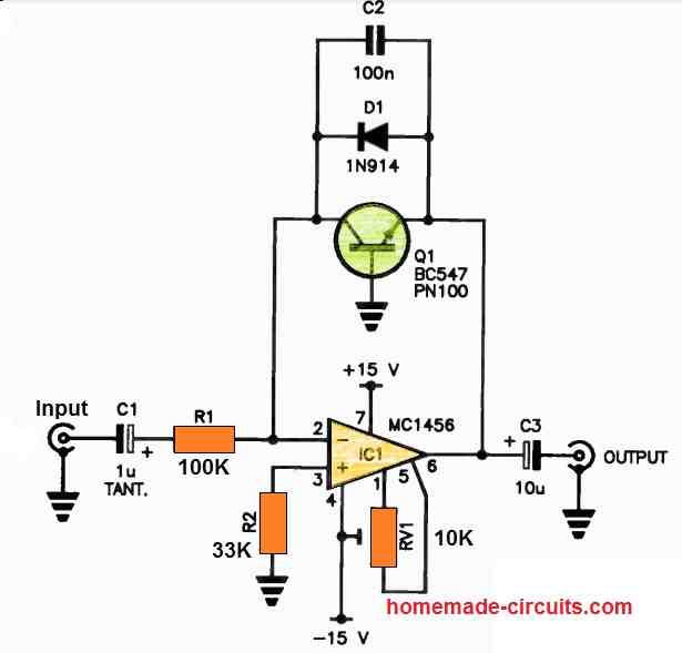
The circuit capitalizes on the logarithmic characteristic inherent in the base-emitter junction of a transistor.
In this setup, the transistor is integrated into the feedback loop of an operational amplifier (op-amp).
Virtually any small-signal transistor can be utilized for this purpose.
Diode D1 is employed to restrict the output voltage swing, while RV1 is finely adjusted to nullify the op-amp's output offset voltage, setting it to zero.
Objective
In this circuit we expect a logarithmic relationship between the input and output signal amplitudes.
Logarithmic Compression:
The circuit compresses a wide range of input signal amplitudes into a smaller output range. For example:
Small input signals get amplified more.
Large input signals get amplified less.
This is due to the logarithmic behavior of the transistors base-emitter junction in the feedback loop.
Dynamic Range Control:
The circuit is well suited for applications like audio compressors or automatic gain control systems where we need to manage signals with a wide dynamic range without distortion.
Output Characteristics:
For small input signals the output will have a relatively larger amplitude.
For larger input signals the output will increase at a slower rate indicating a logarithmic response.
The output should also maintain a clean and low-noise signal if the circuit is correctly designed and components are functioning correctly.
Circuit Working
This circuit works as a logarithmic amplifier by taking advantage of the logarithmic voltage-current relationship of a transistor's base-emitter junction. Let’s understand it step by step:
Input Signal Handling
We start with the input signal which passes through C1 (1 µF). This capacitor blocks any DC component and lets only the AC signal through.
R1 (100 kΩ) sets the input impedance making sure we don’t load the signal source too much.
Operational Amplifier Basics
The MC1456 op-amp is set up in an inverting configuration.
The non-inverting terminal (+) is connected to ground.
The inverting terminal (-) is part of the feedback loop, which includes the transistor (Q1) and the feedback network.
Here the op-amp amplifies the input signal but only as dictated by the components in the feedback loop.
Logarithmic Feedback Using Transistor (Q1)
The key to the logarithmic behavior is Q1 (BC547) whose base-emitter junction gives us a logarithmic relationship between the base-emitter voltage (VBE) and the collector current (IC).
In the feedback loop:
The op-amp makes sure the voltage at the inverting terminal matches the non-inverting terminal (which is at 0 V because of the virtual ground).
This means that the current flowing through the feedback path (via Q1) is directly proportional to the input voltage divided by R1.
The voltage across the transistor’s base-emitter junction VBE adjusts itself to satisfy this current relationship, following the logarithmic formula:
VBE = VT * ln(IC / IS)
Here:
VT is the thermal voltage (about 26 mV at room temperature).
IS is the transistor's saturation current.
Output Signal
At the output, the op-amp gives us a signal thats proportional to the logarithmic response of the feedback loop.
C3 (10 µF) smooths things out by removing any high-frequency noise from the output.
What we get is a signal that’s a logarithmic version of the input which is great for applications like audio compression or analog computation.
Clamping Diode (D1)
D1 (1N914) limits how much the output voltage can swing. This protects Q1 from reverse voltage damage during large input signals.
It also keeps the transistor working within its logarithmic region without going into breakdown or saturation.
Offset Null Adjustment (RV1)
Op-amps naturally have a small offset voltage that can cause an unwanted DC component at the output.
We use RV1 to fine-tune this offset, ensuring the output is zero when the input is zero.
Stabilization with Capacitors
C2 (100 nF) is placed across the diode and transistor to filter out high-frequency noise and stabilize the circuit.
Together with C1 and C3 these capacitors prevent oscillations and ensure smooth, reliable operation.
Conclusion
The input signal goes through R1 to the inverting terminal of the op-amp.
The op-amp adjusts its output to make the base-emitter voltage (VBE) of Q1 follow a logarithmic relationship with the input current.
The output voltage ends up being the logarithmic function of the input, with the swing limited by D1.
RV1 ensures the output starts at zero when the input is zero.


Comments
A clean but heavy, distorted noise with a tide-like swishing sound is produced when the maximum gain is applied. By adjusting the gain from 0 dB up to higher dB levels, the noise-like swishing effect can be smoothly controlled, which helps to create a more pleasing listening experience for the audience. This is a nice circuit to experiment with, and by changing component values you can fine-tune and build up the desired effect.
Thanks for your honest feedback, it is much appreciated!!
Hi, Did someone build the Alternative Logarithmic Compressor ? I can’t make it work at all… Can’t find exact opamp but I tried with TL062, 741 but it doesn’t work. Any suggestion ?
Hi, I have not tried it yet, so can’t confirm the results. By the way did you adjust the offset voltage control to fix a zero output volts, with the input terminal grounded.?
Hi Swag, thanks for you answer. No I did not check the offset but I will. Also I will use maybe an opamp with this function (NE5534 ?)and let you know the result
Thanks Tony! sure, you can try it and let me know how it goes…
Ok, i have some 5534 so i built simple inverting amp to check and my 5534 are ok with offset compensation pot installed. So i set input to ground, set dc offset to zéro. Now i add npn (tried with hfe from 300 to 600, transistor checked before off course), also check 1N914. No way to set dc to zéro this time. I inject 1khz 100mV up to 1 V and i only get a weak and noisy 17 mV on my Clio Pocket audio analyser. How can the npn work with no bias/power supply ? It is supposed to act as à variable résistor ?
Thanks for the update. Yes, The NPN transistor should work like as a variable resistor, controlled by the feedback loop of the op-amp. It doesn’t need a direct power supply. Rather, the op-amp dynamically establishes the base-emitter voltage (around 0.6–0.7 V) to turn it on.
The Weak and Noisy Output could be because the transistor is not conducting properly. Please again verify the feedback loop, diode (1N914), and capacitor connections, and make sure RV1 is adjusted to nullify offsets with the transistor in place.
Are you sure of c2 = 100nf ? Because circuit works without c2 but with 37% thd ! With à small 1nf i get 18%thd with 100mV in, 125 mV out . 1 V in gives only 366 mV out so it compress but with lot of distortion, 25%thd.
Actually these circuits are not designed by me, instead they were contributed by external authors. If reducing C2 value gives better response, then you can reduce it to any desired value.
Makes a cool guitar distortion pedal with a buffer and some gain in front of it. I will explore more and send you final result schematic if i can get à descent result. Anyway, thanks for your help.
Sure, no problem! The final schematic will help the other users to further improve this design.
are there any printed sources you recommend for learning more about audio compressor designs? I have looked at a number of books about audio circuits, but none has more than a passing mention of compressors.
thanks!
Cameron
Currently I am not able to find any external printed sources for this topic, if I happen to find it, i will surely let you know…
Thank you, please do!
for anyone else looking, I did just receive a small book called “Audio IC Projects” that includes a few circuits for VCAs and automatic gain controllers. Not much explanation behind it, just a general overview, schematic, parts list, and pcb layout for people who already have some technical experience.
can i use this circuit also for electric guitar.?
erik
Yes, you can!
parabéns swagatan, fi muito agradecido pela sua imensa generosidade, de compartilhar seus conhecimentos de forma abrangente para todos os estudantes e técnicos eletrônicos em geral.
meus sinceros votos de paz, saúde e felicidade, porque sua ajuda é de extrema importância para o desenvolvimento, e o conhecimento das pessoas que muito precisam de completar ou concluir seus projetos na área eletrônica.
forte abraço.
Fernando Boiago.
Thank you so much Fernando, for your kind words. I greatly appreciate it.
All the best to you.
congratulations to swagatan for the projects presented, your posts are very important for the development of knowledge in
various electronic circuits, for people dedicated to this universe of electronics.
I am immensely grateful for Swagatan’s commitment and dedication to everyone who seeks to improve their knowledge.
thanks!
Thank you so much Fernando, for your kind words. I am glad you found this site helpful.
All the best to you.
Hi Swagatam, regarding the circuit ‘audio clipper with minimum distortion’ that uses the lm394 matched transistors, could you tell me how one can adjust the level at which clipping occurs? I am building a remote microphone for my hearing aids and want to try and stop harsh & sudden noises (such as cutlery banging against plates) from creating discomfort. Many thanks!
Thank You Bob,
Although I am not good with grasping audio circuits, I think R1 and R2 can be tweaked to adjust the clipping thresholds.
Bom dia, se caso montar este compressor, vai funcionar?
If you install the compressor circuit for compressing audio signals, it will work