Both the majority of class B or AB power amplifiers currently encountered in HI-Fi amplifiers are presented in the form of integrated circuits specifically designed for this purpose. It is interesting for technicians to know how this type of amplifier works, if only out of intellectual curiosity.
The provided model allows the study of several different class B and AB amplifier structures. Examining the oscillograms of the output voltage for the various configurations considered enables the user to understand the effect of modifications and their significance.
Classes of Amplification
To define the operating class of a power amplifier, it is sufficient to determine the duration during which the power transistors are conducting in relation to the period of the amplified signals.
When the output stage has a single transistor and it conducts throughout each period, we have a class A amplifier. If the output stage requires 2 complementary transistors that work alternately during half a period, we have a class B amplifier, or more commonly, a class AB amplifier.
The difference between these two classes is related to the biasing of the transistors, which is intended to eliminate the detrimental effects of the base-emitter junction conduction threshold, resulting in connection distortion.
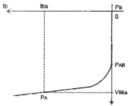
Based on the characteristic curve Ic = f(Vbe) of a silicon NPN transistor, we can say that the three amplification classes A, B, and AB correspond respectively to the operating points PA, PB, and PAB in Figure 1.
For a PNP transistor, the polarities of Ic and Vbe are opposite. Figure 2 below shows the basic diagram of a single-transistor amplifier operating in class A, with base biasing provided by the resistive bridge Ra, Rb.
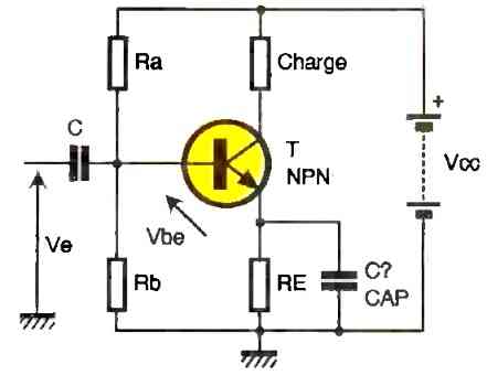
These two components must be calculated so that in the absence of excitation (ve=0), the voltage Vbeo is equal to Vbea (value shown in Figure 1).
The major drawbacks of a class A amplifier are that it consumes significant power even at rest and its maximum efficiency does not exceed 25%.
Therefore, class B and AB amplifiers are preferred, as they have much higher efficiency (up to 78% maximum) and negligible or zero power consumption at rest.
The diagram in Figure 3 below provides the general structure of a class B amplifier without any sophistication.
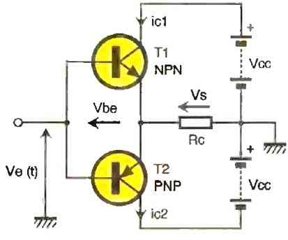
The bases of the two complementary transistors, T1 and T2, are interconnected and connected to the input signal ve(t).
No biasing is provided at the base level, so in the absence of a control signal (ve(t) = 0), the voltage Vbeo is zero.
When ve(t) has a positive alternation with an amplitude greater than the conduction threshold of T1, a collector current ic1 (= β1 * ib1) appears in the load, which can be approximated as equal to the emitter current iel.
During this time, the PNP transistor T2 is in a blocked state. This situation reverses when ve(t) has a negative alternation, with T2 becoming conducting and T1 being blocked.
Due to the voltage drop across the base-emitter junctions, the input voltage ve(t) reappears across the load.
The voltage amplification of a class B stage is slightly less than 1, but its current amplification can be significant since the input and output currents are equal to the base and emitter currents of the transistors.
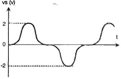
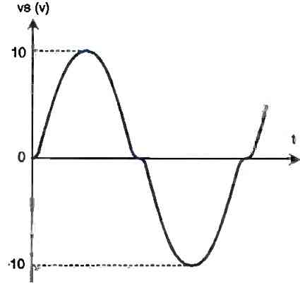
For low-amplitude input voltages ve(t) (a few volts), the conduction threshold of the transistors leads to significant distortion of the output signal, which decreases in relative value as the amplitude of ve(t) increases (Figures 4a and 4b) below.
To reduce this distortion, the bases of the two transistors are slightly biased, and the previous circuit takes the form shown in Figure 5 below.
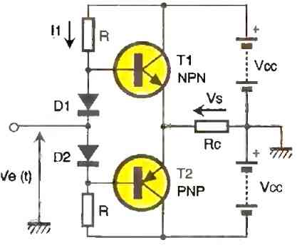
We have an amplifier operating in class AB. The current flow 11 through diodes D1 and D2 creates a voltage drop across them, which biases transistors T1 and T2 at the PAB point (Figure 1).
This pre-biasing eliminates the conduction threshold of the base-emitter junctions of T1 and T2. The output signal vs resembles ve(t).
The term "pre-biasing" is more appropriate than "biasing" because we are operating at a point where the transistor conducts very little or not at all, as it is prepared to conduct.
The transition from class B to class AB only requires a limited number of components to reduce the distortion rate of power amplifiers.
Therefore, it is evident that the vast majority of power amplifiers rely on this structure, which may not always be presented in the proposed form, but its various variations always serve the same purpose.
Characteristics of the Prototype
The prototype is powered by a symmetrical power supply of ±15V with respect to ground, capable of delivering 1A. The load is a 10 Ohm resistor with a minimum rated power of 5W.
Although modest, this significant value already allows us to address several issues related to the heating of the load or power transistors, which are equipped with heat sinks.
The change in structure, transitioning from class B to class AB, requires moving small jumpers similar to those used in computing.
It is worth noting that the power amplifier can also be associated with an operational amplifier to study the improvements brought about by connecting the feedback loop to the load (global feedback).
Prototype Schematic
Figure 6 below represents some of the sub-assemblies discussed in the first part of this article, including transistors T1 and T2.
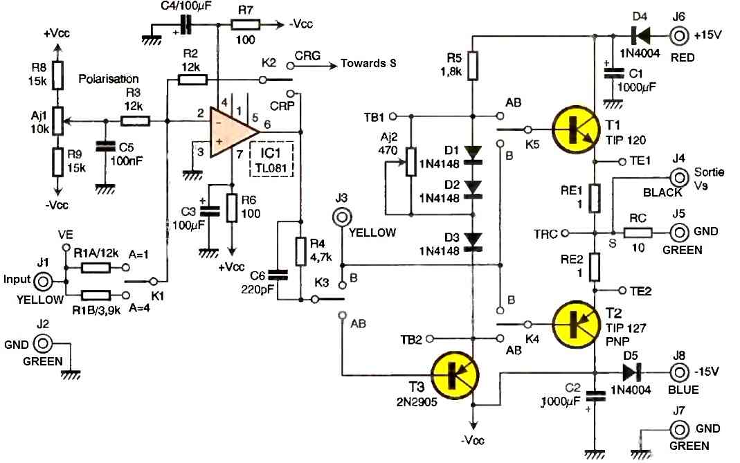
It should be noted that these elements are Darlington transistors (Figure 7 beow), which limits the value of the base current lb since their current gain β exceeds 1000, whereas ordinary power transistors often struggle to reach a β value of 100.
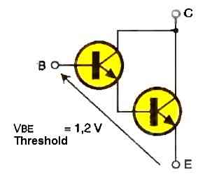
The trade-off of this choice is an increase in the conduction threshold of the transistors (2 times 0.6V), which allows for better evaluation of the flaws of a class B amplifier at low levels but must be taken into account when selecting the biasing system for transitioning to class AB.
Compared to the theoretical diagrams in Figures 3 and 5, we can observe the appearance of two emitter resistors (RE1 and RE2) aimed at stabilizing the operation of the output stage in relation to temperature variations.
Assuming that the emitter current has a value lel at temperature θ1, if the temperature increases while the base current remains constant, the emitter current le increases.
As a result, the power dissipated by the transistor increases, leading to a further rise in temperature. If not properly addressed, this snowball effect can quickly lead to the destruction of the transistor.
By introducing the resistor RE, any increase in the average emitter current reduces the idle voltage Vbeo, and consequently, the base current lb, the emitter current, and the power dissipated by the transistor decrease.
The reduction in power dissipation by the transistor lowers its temperature, compensating for the initial temperature rise.
The biasing circuit for transistors T1 and T2 now involves 3 diodes because the transistors are Darlington pairs, which have a doubled conduction threshold compared to a normal transistor.
In theory, 4 diodes should be connected between the bases of T1 and T2.
However, practical experience shows that using 3 diodes biased at 0.7V provides sufficient pre-biasing for the two transistors, bringing them to approximately 1V (2 times 0.5V).
The goal of pre-biasing is not to put the transistors into conduction but simply to prepare them for conduction. Any over-biasing would lead to unnecessary power dissipation at idle, so the chosen solution is satisfactory.
By adjusting the adjustable resistor Aj2 connected in parallel to D1 and D2, the current passing through these diodes can be modified.
This alters the voltage drop across the diodes, allowing for better adjustment of the inter-base voltage of T1 and T2.
The biasing circuit is connected to the emitter of transistor T3, whose base receives the output signals from the operational amplifier (OP-AMP) IC1.
The OP-AMP is configured as an inverting adder (or potentially an amplifier for input signals when using resistor R1b instead of R1a).
One of the inputs of IC1 receives a bias voltage (adjustable by Aj1), while the second input receives the signal to be amplified (ve(t)).
When the maximum amplitude of the signals provided by the function generator (GBF) supplying this prototype does not exceed 5V, these signals are amplified (3 times=R2/R1b) by setting the jumper switch K1 downwards.
If the GBF provides a signal with an amplitude of at least 10V, this amplification is unnecessary, and K1 is positioned upwards (amplification -R2/R1a=-1).
The feedback resistor (R2) of the OP-AMP can be directly connected to its output (jumper switch K2 in the lower position = partial feedback, CRP) or to the hot point (S) of the load resistor Rc (global feedback, CRG).
To conclude the specific features of this OP-AMP stage, its power supply is provided through resistors R6 and R7, decoupled respectively by capacitors C3 and C4.
These low-pass filters aim to reduce any potential fluctuations in the high-power general supply voltage.
Without this precaution, parasitic oscillations could occur in the circuit, especially if the power source is slightly limited in current.
Similarly, the ±15V power lines are decoupled by capacitors C1 and C2 with high capacitance values.
The capacitor C6, connected in parallel to R4 (base resistor of T3), reduces the risk of high-frequency oscillations in this circuit, which has high current gain. Diodes D4 and D5 serve as protection in case of reverse polarity on the power supply.
Practical implementation
The printed circuit board (PCB), whose layout is shown in Figure 8 below, supports all the components of the circuit.
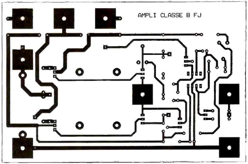
Its wiring poses no difficulty; it is sufficient to follow the proposed arrangement as shown in Figure 9 below.
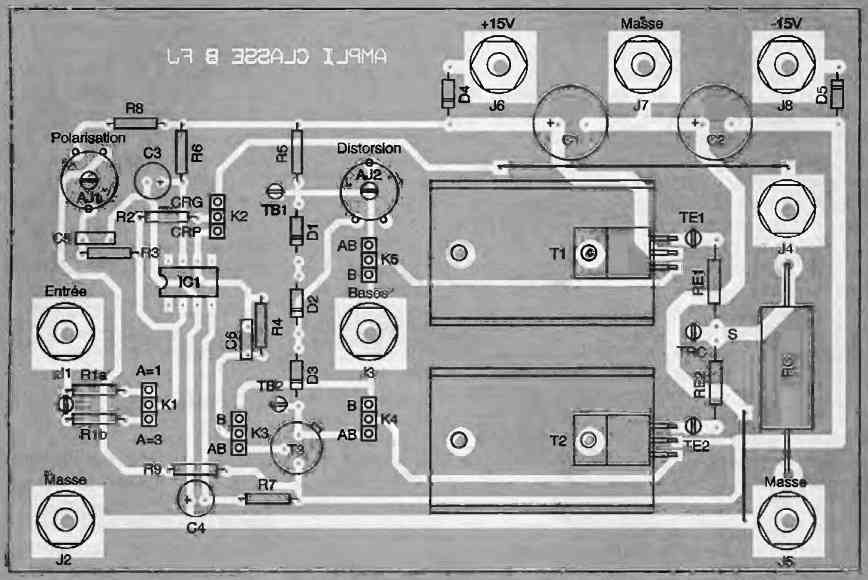
The implementation of the "switches" that enable the structural change involves using breakable male pin headers with a 2.54 mm pitch.
Three pins are required per switch. The power transistor heat sinks are TV21 models secured in place with 3 mm diameter screws.
The positioning of the transistors on these heat sinks requires careful drilling during assembly.
To facilitate thermal exchange, it is advisable to raise resistors RE1, RE2, and load resistor Rc by at least one millimeter relative to the PCB.
The various 4 mm female terminals for the chassis allow for connections with the external world (function generator, DC power supply). Several test points (TB1, TE1, etc.) enable the visualization of signals at different points in the circuit.
How to Use
Primarily intended to highlight the various aspects of power amplification in class B and class AB, this circuit offers numerous measurement possibilities: observing the waveform at different points in the circuit for different configurations, measuring distortion levels, current consumption, output power, calculating efficiency, and determining operating limits, among others.
Several measurements can be performed for different configurations, such as analyzing and measuring the distortion level of the output signal, determining the maximum input level that causes saturation in at least one of the output transistors, measuring the output power (Ps) and the absorbed power (Pf) by the circuit, and calculating the efficiency.
Observing the signals naturally requires the use of an oscilloscope.
Measuring distortion levels can rely on the study of switched capacitor filter circuits, which we have discussed and used in previous months.
Measuring the output power (Ps) follows the formula Ps = Vs²eff / Rc. To accurately measure it, a true RMS voltmeter should be connected across the load resistor (Rc), especially when the output signal is not sinusoidal, as is the case with uncompensated class B amplification.
With a load resistor value of 10 ohms, an effective voltage of 7V (corresponding to a peak value of 10V in a sinusoidal regime) is required to achieve a power of 5W at the load.
To measure the power supplied by the power sources (Pf = Vcc(I* + I)), a DC ammeter should be inserted between each power source and the circuit.
Knowing Ps and Pf allows for the calculation of the circuit's efficiency (η = Ps/Pf).
The maximum theoretical efficiency of a class B amplifier is 78%, although it is unlikely to be achieved in practice (unless there are measurement or calculation errors).
Deviations from theory can be attributed to transistor threshold voltages, non-zero Vcesat values, and the presence of emitter resistances that are not considered in the theoretical calculation of maximum efficiency.
It is important to note that the operational amplifier stage introduces a phase shift of 180° when in use, which is normal since it operates as an inverter.
Different Configurations
Whenever the operational amplifier IC is used, it is important to note that the DC bias introduced by the adjustable resistor Aj1 affects the operating point of the power stage.
Therefore, it is necessary to verify that the voltage Vs across the load is zero at rest for each configuration change.
The basic class B amplifier (similar to the circuit in Figure 3 but with additional emitter resistors) can be obtained by setting jumpers K4 and K5 towards input terminal J3.
If the function generator (GBF) delivers a signal with an amplitude of at least 10y, it can be directly connected to this input (J3) and to the ground, ensuring that jumper K3 is removed or placed in the down position to avoid coupling the GBF signal to the output of the operational amplifier IC1.
If the amplitude of the GBF output signal is insufficient, it can be sent to input terminal J1 and amplified by setting jumper K1 to the down position.
Don't forget to place jumper K2 downwards (CRP) and K3 upwards to allow the IC1 output signal to reach terminal J3.
To observe the effect of overall feedback (as shown in the theoretical schematic in Figure 10 below), simply move jumper K2 upwards.
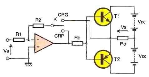
This modification has a significant impact on the shape of the output signal, which appears to have no distortion even at low levels.
This particular configuration lowers the transistor conduction threshold to a value equal to Vseui I/A, where A represents the open-loop amplification of the operational amplifier IC1.
With A approximately equal to 100,000, transistors T1 and T2 begin conducting as soon as the input voltage exceeds a few μV.
This value is so small that the conduction appears constant to the observer. In this specific configuration, the voltage amplification VsNe of the circuit is equal to -R2/R1, with the combination of the operational amplifier and the class B amplifier forming a power operational amplifier.
The transition from class B to class AB is achieved by modifying the positions of jumpers K3, K4, and K5. The first jumper is moved downwards, while the other two are placed as far away as possible from terminal J3.
The signal to be amplified is applied to terminal J1. When choosing this configuration, start by adjusting Aj1 so that the output voltage Vs is zero at rest.
Then apply a sinusoidal signal Ve(t) and observe the influence of the adjustment of Aj2 on the shape of the output signal.
Once the crossover distortion is properly compensated, it is advisable to recheck the quiescent point of the output stage.
Adjust Aj1 if Vs is non-zero while ve(t) is zero. Also, ensure that the voltage drop across the two emitter resistors RE1 and RE2 does not exceed 10 or 20mV (corresponding to emitter currents of 10 or 20mA).
If it does, it indicates that the transistors are not correctly biased. In such a case, readjusting Aj2 may be necessary, even if it slightly affects the quality of the output signals.
This slight deterioration can be compensated by using overall feedback instead of partial feedback (via K2).
It is important to emphasize that any configuration change must be accompanied by readjusting the quiescent point of the output stage using Aj1.
Without this precaution, transistors T1 and T2 may heat up abnormally, even in the absence of any signal at the input of the circuit.
These guidelines should help users understand the advantages of different configurations relative to others and provide a better understanding of the operation of class B and class AB power amplifiers.


Need Help? Please Leave a Comment! We value your input—Kindly keep it relevant to the above topic!