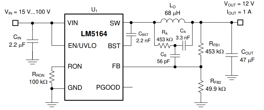
Ok now we have this LM5164 chip, and we want to drop voltage from 100V down to let's say 12V, right? But we also need 1A output so we need to design everything properly. Now this chip is cool because it has ultra-low quiescent current (IQ) so it does not waste much power when it is idle. Also this is a synchronous buck converter, which means that it has MOSFETs inside, so we do not need an external diode like old-school buck circuits. That makes it more efficient.
Now here we first see the circuit with LM5164 then we go step by step choosing parts like inductor, capacitor, resistors and finally, we talk about PCB layout and troubleshooting. Ok, let’s start.
What We Get with LM5164
This LM5164 chip is super useful because it can take 15V to 100V input, and we can set output voltage from 1.225V to whatever we want (below VIN). But here we set it at 12V 1A. Now some good things about this chip:
Works from 15V to 100V so very flexible.
We can adjust output using two resistors.
Gives 1A current, good enough for many things.
Has low IQ so doesn’t waste much power.
Uses constant-on-time (COT) control, meaning fast response to load changes.
Has MOSFETs inside so no need for external diodes.
So this chip is pretty neat when we want high voltage input but need a safe 12V output.
What This Circuit Has
Now when we use this LM5164 we do not just connect it directly, we need other parts to make it work properly. Here is what we put:
LO (Inductor) → This part stores energy and helps switching work smoothly.
CIN (Input capacitor) → This stabilizes input voltage so that LM5164 doesn’t see sudden voltage dips.
COUT (Output capacitor) → This reduces ripple, so we get clean 12V DC.
RFB1, RFB2 (Feedback resistors) → These set output voltage.
CBST (Bootstrap capacitor) → This helps the high-side MOSFET work properly.
RA, CA, CB (Compensation network) → These are needed to keep the circuit stable.
If we choose wrong values, then we get bad output—either voltage jumps, high ripple, or it won’t even start. So, we calculate everything properly.
How We Set Output Voltage
Now LM5164 has a feedback pin (FB) and we connect RFB1 and RFB2 there to set the output voltage. The formula is:
VOUT = 1.225V * (1 + RFB1 / RFB2)
We fix RFB2 = 49.9kΩ (good value from datasheet), now we calculate RFB1 for 12V output:
RFB1 = (VOUT / 1.225V - 1) * RFB2
RFB1 = (12V / 1.225V - 1) * 49.9kΩ
RFB1 = (9.8 - 1) * 49.9kΩ
RFB1 = 8.8 * 49.9kΩ
RFB1 = 439kΩ
Ok but 439kΩ is not standard so we use 453kΩ which is close enough.
How Fast This Circuit Switches
This buck converter works by switching, so we need to set switching speed. The time it stays on (TON) is:
TON = VOUT / (VIN * fSW)
We take VOUT = 12V, VIN = 100V, fSW = 300kHz so:
TON = 12V / (100V * 300000)
TON = 400ns
Now the off-time (TOFF) is:
TOFF = TON * (VIN / VOUT - 1)
Substituting values:
TOFF = 400ns * (100V / 12V - 1)
TOFF = 400ns * 7.33
TOFF = 2.93µs
The duty cycle (D) is:
D = VOUT / VIN
D = 12V / 100V
D = 0.12 (12%)
So the MOSFET is on for 12% time and off for 88% time.
Choosing Components
Inductor (LO)
We find LO using this:
LO = (VINmax - VOUT) * D / (ΔIL * fSW)
We take ΔIL = 0.4A,
LO = (100V - 12V) * 0.12 / (0.4A * 300000)
LO = 68µH
So we use a 68µH inductor.
Output Capacitor (COUT)
We need COUT to reduce ripple:
COUT = (IOUT * D) / (ΔVOUT * fSW)
For ΔVOUT = 50mV,
COUT = 8µF
But better to use 47µF to be safe.
Input Capacitor (CIN)
For CIN we use:
CIN = (IOUT * D) / (ΔVIN * fSW)
For ΔVIN = 5V,
CIN = 2.2µF
Bootstrap Capacitor (CBST)
We just take 2.2nF from the datasheet recommendation.
Checking Efficiency
Efficiency (η) is:
η = (Pout / Pin) * 100%
Pout = VOUT * IOUT = 12W
For 80% efficiency,
Pin = 12W / 0.80 = 15W
Input current:
IIN = Pin / VIN
IIN = 15W / 100V
IIN = 0.15A
PCB Layout, Super Important!
Now if PCB layout is bad then we get high noise, bad performance or even failure. So:
Make high-current traces short and wide.
Place capacitors close to the chip.
Use a ground plane to reduce noise.
Add thermal vias under the LM5164 to help cooling.
Testing and Fixing Problems
Start with low input voltage (15V).
Check if we get 12V output.
Use an oscilloscope to see switching waveform.
Increase VIN up to 100V and check for heating.
If Things Go Wrong
| Problem | Why? | Fix |
|---|---|---|
| No output | Wrong feedback resistors | Check RFB1, RFB2 |
| High ripple | Bad capacitor | Use low-ESR capacitor |
| Overheating | Bad layout | Improve cooling |
Build This LM5164 Circuit Like a Pro, Step by Step
now we know how to design the LM5164 buck converter but if we build it carelessly, then boom! It won’t work or it will get hot, or output will be noisy. So now we go deep into construction tips to make this solid, stable, and reliable. If we follow all these then this circuit will work like a charm.
PCB Design – If We Mess This Up, Nothing Will Work
Ok, PCB layout is super, super important. If we do it badly then we get high noise, poor efficiency, overheating, and unstable voltage. Heres how we do it correctly:
Keep High-Current Paths Short and Thick
Now the current is super high in some places especially from VIN to SW, through the inductor, so these traces must be wide and short.
If these traces are thin or long then resistance increases, heat increases, voltage drop happens, and efficiency goes down.
So we use at least 50 mil (1.2 mm) width for high-current traces.
Place Capacitors Very Close to LM5164
CIN (input capacitor) and COUT (output capacitor) must be as close as possible to the LM5164 pins.
If they are far away then parasitic inductance comes in, voltage spikes happen, and switching becomes noisy.
So we directly place CIN between VIN and GND pin of LM5164.
We directly place COUT near the load so that output stays clean.
Grounding Must Be Perfect – Use Ground Plane
Bad grounding means noise, ripple and instability.
We do not use thin ground traces. Instead we use a full ground plane on the bottom layer.
All capacitors must be grounded directly to this ground plane, not through thin traces.
This reduces noise and improves efficiency.
Keep FB (Feedback) Trace Away from Switching Node
The FB pin is super sensitive. If we let it pick up noise then output voltage jumps up and down randomly.
So we route FB trace far away from the SW node.
We use a small via to take FB trace to the bottom layer so it stays away from noisy signals.
Thermal Considerations – Keep LM5164 Cool
If LM5164 gets hot, efficiency goes down and it might even shut down.
The GND pad of LM5164 should have multiple thermal vias connecting it to the bottom copper layer.
We can also use a small copper area (heat sink) around the chip to help cool it down.
Soldering – If We Do It Wrong, It is Dead
Ok, now we have the PCB ready but if we don’t solder properly then this thing won’t work or worse, it will burn.
Use Proper Soldering Iron and Tip
LM5164 is an SMD component so we don’t use a big fat soldering iron.
A small tip (1mm) with temperature around 300°C is perfect.
If we go too hot then we burn the chip. If we go too cold, then solder joints will be bad.
Use Flux – Always, No Excuse
Flux is super important because it removes oxidation and makes solder flow properly.
We apply a little flux before soldering so that joints are shiny and strong.
If we do not use flux then we get cold joints and then circuit wont work properly.
Solder LM5164 First, Then Other Parts
We first solder LM5164 properly because it is the most important component.
Then we solder all capacitors because they stabilize everything.
Then we solder resistors and inductor.
Testing After Soldering – If We Skip, We Might Burn It
Now before we power it up we must check some things or else we might see smoke.
Check for Short Circuits
We take a multimeter, set it to continuity mode and check:
VIN to GND (should NOT beep or we have a short!)
SW to GND (should NOT beep, or MOSFET is shorted!)
VOUT to GND (should have resistance, but not zero!)
Apply Power Slowly – Do not Jump to 100V
We don’t just connect 100V right away! We first test with 15V or 20V.
If output is 12V as expected then we slowly increase input voltage step by step.
If voltage jumps or heating starts or weird noise comes, we stop and check what’s wrong.
Check Waveforms with an Oscilloscope
We take a scope and check:
SW node (should show clean square waves, no ringing)
VOUT (should be smooth, no high ripple)
FB pin (should be stable, no oscillations)
Fixing Problems – If Things Go Wrong
Ok even if we do everything right, still sometimes things don’t work. So, here’s how we debug issues:
| Problem | Why It Happens | Fix |
|---|---|---|
| No output voltage | Feedback resistors wrong | Check RFB1, RFB2 values |
| Output voltage too high | FB pin picking noise | Route FB trace away from SW node |
| High ripple on output | Bad output capacitor | Use low-ESR capacitor (47µF MLCC) |
| Overheating | Bad PCB layout | Add thermal vias, widen traces |
| Noisy switching waveform | Poor grounding | Use full ground plane |
| Circuit not starting | Bootstrap capacitor wrong | Use 2.2nF CBST |
Final Thoughts
So we designed the full 100V to 12V buck converter using LM5164, picked all the right components and made sure it is efficient and stable. If we follow good PCB design then it works perfectly. This chip is great for industrial, automotive, and battery applications where we need safe, low voltage from high input.
Original source:


Comments
Hello Mr. Swagatam
Thank you for answering questions, and I thank you in advance for answering my question.
I want to convert 12V DC to 1 to 5 volts DC with a power of 3000 watts and with very low power loss.
Please send the circuit schematic.
Thank you.
Hi Mazloumi, for that your 12V source must be rated at 3000/12 = more than 250 amps, do you have this arrangement?
yes Mr. Swagatam.
I want to have electromagnets whose pole directions are reversed every few seconds,perfectly synchronized with each other via an H-bridge. I will determine the number of magnets through practical testing.
Perhaps twenty will be needed.I want to apply 1 to 5 volts and 120 amps to each magnet. If it’s possible with 1 volt, I would definitely use 1 volt. If not, I will increase the voltage. Mr. Ali, in your opinion, how can I synchronize these magnets exactly with each other? I might need up to 30 of them. For example, can I have a separate H-bridge for each electromagnet but use one common driver for all of them?
Yes, Mr. Swagatam. my input power supply is 12V DC and at least 250 amps, and the preferred output is 1 volt and 3000 watts. However, the output voltage should be adjustable up to 5 volts without a drop in power and with high efficiency.
Thank you for your efforts and guidance.
best regards.
Thank you Mazloumi,
In that case you will need to design your own customized buck converter using the following software:
https://www.homemade-circuits.com/buck-converter-calculator/
For the core you can use any large E-core with thick Litz wire, the wire thickness can be calculated using the following calculator:
https://www.homemade-circuits.com/56492-2/
Hello Mr. Swagatam
Thanks of your reply.
Mr Swagatam , in your opinion, how can I synchronize these magnets exactly with each other? I might need up to 30 of them. For example, can I have a separate H-bridge for each electromagnet but use one common driver for all of them?
best regards
Mr. Mazloumi, do you want the magnetization to happen in rotating form, where opposite magnets have opposite polarity?
Yes.
Should they all have the North pole or the South pole simultaneously and occur in a rotating manner,where opposite magnets have opposite polarity?
Also, if I apply, for example, 1 volt and a current of 50 amperes to each electromagnet, do you think they will work? Because the voltage is very low. Won’t this voltage level cause any issues in the system’s operation? According to my own calculations, there is no problem regarding wire resistance in the design, and it is possible to pass even more current.
If your electromagnet winding is rated to work with 5V, 50 amp then it won’t have any problems…
Since, i do not have any expertise in this concept, it may be difficult for me to guide you with this project.
That said, if you have any further questions regrading this specific project, please feel free to post them under the following article, I will try my best to solve them for you…
https://www.homemade-circuits.com/regenerative-motor-acceleration-experiment/
When you look at these DC to AC inverters, they have as many as 8 transformers inside them, there circuits are simple there is no extra stuff. I have a project that uses 4 HF ee42 transformers rated at 1000 watts each. They have a bunch of voltage output from 50 to 420 volts. I pick a tap say 220 ac. After a full bridge and a cap, I end up with 245 volts but none of them are the same output I parallel them, there is failure at some time some times right away. Maybe this is so simple and I am crazy. I question myself. Thanks.
Hey Art, as you can see your comment is not related to the above buck converter article…so can please post your question again under a transformer or inverter related article…I will try to solve it for you…