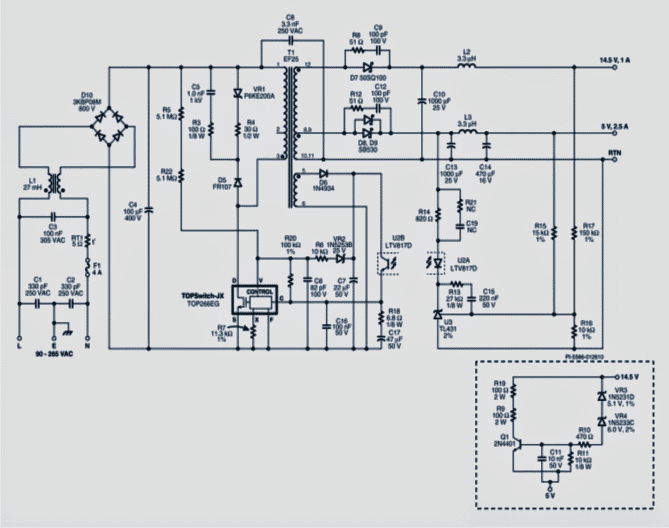
This power supply functions with a broad input voltage range from 90 to 265 V AC and produces a dual output in the form of 5 V / 2.5 A, and 14.5 V / 1 A.
The Circuit Layout
The great aspect of this source is its minimal power consumption, optimized power consumption in idle mode and high efficiency at full load conditions.
There are additional built in security protections, which includes hysteretic output overvoltage protection, hysteretic output protection against short circuit and thermal protection against overheating with a large hysteresis.
Part of the below given explanation is a comprehensive power supply specifications, schematic overview and components used, along with manufacturing documentation and proposal transformer circuit boards and a summary of performance data.
The power supply circuit uses the TOPSwitch-JX TOP266EG (U1), which directly hooks up in its housing and also with the high voltage switching MOSFET and driver flyback configuration.
EMI Filter
Capacitors C1, C2 and C3 in conjunction with the inductance L1 forms an EMI filter, which works both in the common mode and differential mode EMI filtering.
It is followed by the subsequent classic diode bridge D10, which rectifies the input AC voltage, and the resulting power is further filtered by capacitor C4. A diode bridge was selected in the form of D10 in order to execute a reliable operation even at lower input potentials such that it compensates and operates at full load.
Using the IC TOP266EG
TOP266EG circuit (U1) TOPSwitch-JX Series shakes hand with oscillator circuit driver switching element, trigger and protection circuitry and MOSFET power supply - all within a single monolithic IC.
One of the terminals of the primary winding of the power transformer T1 can be seen joined to the positive side of the filter capacitor C4 and the other line gets hooked up directly with the output pin of U1. When the attached MOSFET turns off, the leakage inductance of the transformer peaks up to induce voltage.
The specified amplitude is restricted by the clamping stage, consisting of D5, R4, VR1, R3 and C5.
A big portion of the excess energy becomes avaialble across VR1 and R4 is a series combination of R3 and C5 (parallel with R4 and VR1), which further contributes to minimize the magnitude of high frequency surges.
The value of the resistor R4 fixes the magnitude of the difference between the two channels. This framework was implemented for minimizing switching losses and internal consumption while it may be running on without any load.
Circuit Diagram
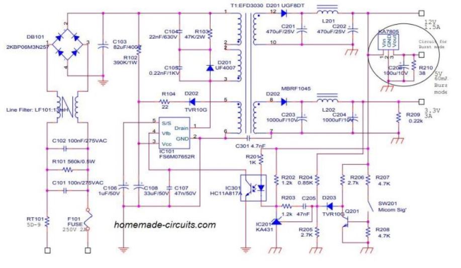
Another design using Fairchild's FPS switch:
FOR COMPLETE DETAILS REFER TO THIS ARTICLE


Questions & Answers
I did. some said 100KHz max, 500KHz max for the bipolar type and 2MHz max for the cmos type. I m having only d bipolar type available(NE555). pls can u help me test it live with your oscilloscope. r1=1k, r2=100k and c=10pF. please help me out. tanx
600 kHz is achievable if done carefully by using high quality components and by keeping all the leads as short as possible, use SMD parts preferably.
your part values will produce above 700kHz and at 50% duty cycle.
Can an NE555 oscillate @ a frequency of 600KHz, 50% duty cycle if r1=0.5 ohms r2=12k and c=100pF? If not, help me 2 verify it, i dont have an oscilloscope.
I am not sure whether the the part values suggested by you are correct or not, but the idea is possible….just Google "555 circuit with 50% duty cycle" once you have located the circuit, you can simple change the capacitor value for achieving the desired frequency….you can use any online 555 calculator for calculating the capacitor value that would give 600khz.