Referring to the following chaser circuit diagram below, we can see a low-frequency, astable oscillator circuit, made up of two gates, IC1a and IC1b, from the IC 4011 quad two-input NAND gate.
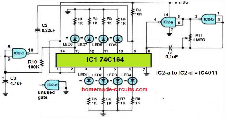
The operating frequency of this astable is determined by the values of C1 and R11. This circuit configuration works well as a clock-pulse generator for feeding the IC1's 74C164 shift register. The positive output pulses from the clock at pin 4 of IC2 are supplied into the shift register's clock input at pin 8 of IC1.
Each output of the shift register is wired to an LED. Each LED is connected to a 1K current-limiting resistor in series.
The input of gate IC2c is connected to the eighth output of the shift register, located at pin 13, via a time-delay RC configuration comprised of R10 and C3.
The output of the gate is connected to the clear input of the shift register at pin 9 through a capacitor. LED8 is turned on by the eighth clock pulse, and C3 is charged as soon as pin 13 of IC1 becomes positive.
After a little delay, the output of IC2c becomes low, clearing the outputs of the shift register.
The LEDs light up in the following sequence: LED1 is turned on by the first clock pulse, LED2 by the second, and so forth until all eight LEDs are illuminated.
The clear pulse from IC2c shuts off each LED once the eighth LED illuminates, and the process is then repeated.
R10 and C3's values can be changed to make LED8 stay on for the identical amount of time as the remaining LEDs.
For a quicker sequence, the RC time delay circuit must be smaller; and for a slower series, it must be larger. Increasing the value of R10 or C3 will shorten the delay period, and decreasing the value will extend the delay time.
Explanation in Details
This circuit is basically one LED chaser using 74C164 Shift Register so LEDs keep turning ON one after another. When the last LED lights up then the whole thing resets again and starts from beginning.
Astable Clock Generator
IC2 works like an astable oscillator here which means it keeps generating clock pulses continuously by itself.
Pulse speed depends mainly on R11 and C1, so if R11 or C1 becomes larger then pulses slow down but if values become smaller then pulses speed up.
Those pulses come from pin 4 of IC2 and go into pin 8 of IC1 which is the clock input of the shift register. so now every pulse acts like one step movement command.
Shift Register Operation
The 74C164 Shift Register keeps shifting one logic HIGH from one output to next output whenever clock pulse arrives.
Outputs are connected to LEDs through 1K resistors because resistors limit current otherwise LEDs and IC outputs may take too much current.
So first pulse turns ON LED1, then next pulse shifts things forward and LED2 turns ON, then LED3 after that, and it keeps moving like this until LED8 finally turns ON after the eighth pulse.
Outputs remain latched meanwhile therefore LEDs look like they are filling one by one gradually.
Reset Delay Circuit (R10 and C3)
Now the last output pin 13 is connected into IC2c through R10 and C3 and this section mainly creates a small delay before reset happens.
When LED8 turns ON then pin 13 becomes HIGH and C3 starts charging through R10 slowly.
After a short moment voltage across C3 rises enough, then IC2c changes its output state and sends one reset pulse into pin 9 of the shift register which is the clear input.
As soon as pin 9 gets that clear pulse then all outputs instantly become LOW and all LEDs switch OFF together.
Clock however still keeps running, so sequence starts again from LED1.
Why the Delay is Needed
Without R10 and C3 the reset would happen almost immediately so LED8 may barely become visible before everything resets again.
That little RC delay keeps LED8 ON briefly so it looks normal like the other LEDs instead of disappearing too quickly.
Adjusting the Chase Speed
We have actually two timing sections here.
Main running speed comes from R11 and C1, those decide how fast LEDs move from one output to another.
Then reset delay comes from R10 and C3 which decides how long LED8 stays ON before reset occurs.
So now if you increase R10 or C3 then delay becomes longer and LED8 stays visible more time.
If values are reduced then reset happens faster.
Important Timing Clarification
Normally in RC timing circuits we see larger R or C values produce larger delay, while smaller values reduce the delay time So if someone wants LED8 to stay ON longer then increase R10 or C3.
If faster reset is needed then decrease them.
That previous statement saying increasing R10 or C3 shortens delay looks technically opposite maybe, because practically RC delay normally increases when resistance or capacitance increases.


Need Help? Please Leave a Comment! We value your input—Kindly keep it relevant to the above topic!