In this post we try to investigate how to design a SG3525 full bridge inverter circuit by applying an external bootstrap circuit in the design. The idea was requested by Mr. Mr. Abdul, and many other avid readers of this website.
Audio/Video Representation
Why Full-Bridge Inverter Circuit is not Easy
Whenever we think of a full bridge or an H-bridge inverter circuit, we are able to identify circuits having specialized driver ICs which makes us wonder, isn’t it really possible to design a full bridge inverter using ordinary components?
Although this may look daunting, a little understanding of the concept helps us realize that after all the process may not be that complex.
The crucial hurdle in a full bridge or a H-bridge design is the incorporation of 4 N-channel mosfet full bridge topology, which in turn demands the incorporation of a bootstrap mechanism for the high side mosfets.
What's Bootstrapping
So what’s exactly a Bootstrapping Network and how does this become so crucial while developing a Full bridge inverter circuit?
When identical devices or 4 n-channel mosfets are used in a full bridge network, bootstrapping becomes imperative.
It's because initially the load at the source of the high side mosfet presents a high impedance, resulting in a mounting voltage at the source of the mosfet. This rising potential could be as high as the drain voltage of the high side mosfet.
So basically, unless the gate/source potential of this mosfet is able to exceed the maximum value of this rising source potential by at least 12V, the mosfet won't conduct efficiently. (If you are having difficulty understanding please let me know through comments.)
In one of my earlier posts I comprehensively explained how emitter follower transistor works, which can be exactly applicable for a mosfet source follower circuit as well.
In this configuration I have explained that the base voltage for the transistor must be always 0.6V higher than the emitter voltage at the collector side of the transistor, in order to enable the transistor to conduct across collector to emitter.
If we interpret the above for a mosfet, we find that the gate voltage of an source follower mosfet must be at least 5V, or ideally 10V higher than the supply voltage connected at the drain side of the device.
If you inspect the high side mosfet in a full bridge network, you will find that the high side mosfets are actually arranged as source followers, and therefore demand a gate triggering voltage that needs to be a minimum 10V over the drain supply volts.
Once this is accomplished we can expect an optimal conduction from the high side mosfets via the low side mosfets to complete the one side cycle of the push pull frequency.
Normally this is implemented using a fast recovery diode in conjunction with a high voltage capacitor.
This crucial parameter wherein a capacitor is used for raising the gate voltage of a high-side mosfet to 10V higher than its drain supply voltage is called bootstrapping, and the circuit for accomplishing this is termed as bootstrapping network.
The low side mosfet do not require this critical configuration simply because the source of the low side mosets are directly grounded. Therefore these are able to operate using the Vcc supply voltage itself and without any enhancements.
How to Make a SG3525 Full Bridge Inverter Circuit
Now since we know how to implement a full bridge network using bootstrapping, let’s try to understand how this could be applied for achieving a full bridge SG3525 inverter circuit, which is by far one of the the most popular and the most sought after ICs for making an inverter.
The following design shows the standard module which may be integrated to any ordinary SG3525 inverter across the output pins of the IC for accomplishing a highly efficient SG3525 full bridge or H-bridge inverter circuit.
Please use this online calculator to calculate the SG3525 parameters.
Circuit Diagram
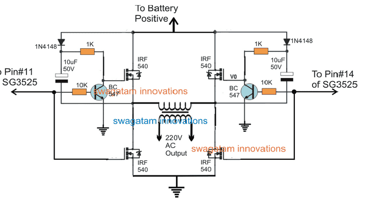
Referring to the above diagram, we can identify the four mosfets rigged as an H-bridge or a full bridge network, however the additional BC547 transistor and the associated diode capacitor looks a bit unfamiliar.
To be precise the BC547 stage is positioned for enforcing the bootstrapping condition, and this can be understood with the help of the following explanation:
We know that in any H-bridge the mosfets are configured to conduct diagonally for implementing the intended push pull conduction across the transformer or the connected load.
Therefore let’s assume an instance where the pin#14 of the SG3525 is low, which enables the top right, and the low left mosfets to conduct.
This implies that pin#11 of the IC is high during this instance, which keeps the left side BC547 switch ON. In this situation the following things happen withing the left side BC547 stage:
1) The 10uF capacitor charges up via the 1N4148 diode and the low side mosfet connected with its negative terminal.
2) This charge is temporarily stored inside the capacitor and may be assumed to be equal to the supply voltage.
3) Now as soon as the logic across the SG3525 reverts with the subsequent oscillating cycle, the pin#11 goes low, which instantly switches OFF the associated BC547.
4) With BC547 switched OFF, the supply voltage at the cathode of the 1N4148 now reaches the gate of the connected mosfet, however this voltage is now reinforced with the stored voltage inside capacitor which is also almost equal to the supply level.
5) This results in a doubling effect and enables a raised 2X voltage at the gate of the relevant mosfet.
6) This condition instantly hard triggers the mosfet into conduction, which pushes the voltage across the corresponding opposite low side mosfet.
7) During this situation the capacitor is forced to discharge quickly and the mosfet is able to conduct only for so long the stored charge of this capacitor is able to sustain.
Therefore it becomes mandatory to ensure that the value of the capacitor is selected such that the capacitor is able to adequately hold the charge for each ON/OFF period of the push pull oscillations.
Otherwise the mosfet will abandon the conduction prematurely causing a relatively lower RMS output.
Well, the above explanation comprehensively explains how a bootstrapping functions in full bridge inverters and how this crucial feature may be implemented for making an efficient SG3525 full bridge inverter circuit.
Now if you have understood how an ordinary SG3525 could be transformed into a full fledged H-bridge inverter, you might also want to investigate how the same can be implemented for other ordinary options such as in IC 4047, or IC 555 based inverter circuits, …..think about it and let us know!
UPDATE: If you find the above H-bridge design too complex to implement, you may try a much easier alternative
SG3525 Inverter Circuit which can be Configured with the the above Discussed Full Bridge Network
The following image shows an example inverter circuit using the IC SG3525, you can observe that the output mosfet stage is missing in the diagram, and only the output open pinouts can be seen in the form of pin#11 and pin#14 terminations.
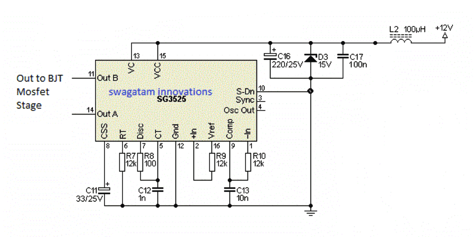
The ends of these output pinouts simply needs to be connected across the indicated sections of the above explained full bridge network for effectively converting this simple SG3525 design into a full fledged SG3525 full bridge inverter circuit or an 4 N channel mosfet H-bridge circuit.
Feedback from Mr. Robin, (who is one of the avid readers of this blog, and a passionate electronic enthusiast):
Hi Swagatum
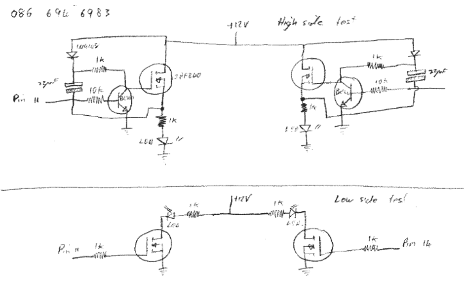
Ok,just to check everything is working I separated the two high side fets from the two low side fets and used the same circuitry as:
(https://www.homemade-circuits.com/2017/03/sg3525-full-bridge-inverter-circuit.html),
connecting the cap negative to the mosfet source then connecting that junction to a 1k resistor and an led to ground on each high side fet.Pin 11 pulsed the one high side fet and pin 14 the other high side fet.
When I switched the SG3525 on both fets lit up momentarily and the oscillated normally thereafter.I think that could be a problem if I connected this situation to the trafo and low side fets?
Then I tested the two low side fets,connecting a 12v supply to a (1k resistor and an led) to the drain of each low side fet and connecting the source's to ground.Pin 11 and 14 was connected to each low side fets gate.
When I switched the SG3525 on the low side fet's would not oscillate until I put a 1k resistor between the pin (11, 14) and the gate.(not sure why that happens).
Circuit diagram attatched below.
My Reply:
Thanks Robin,
I appreciate your efforts, however that doesn't seem to be the best way of checking the IC 's output response...
alternatively you can try a simple method by connecting individual LEDs from pin#11 and pin#14 of the IC to ground with each LED having its own 1K resistor.
This will quickly allow you to understand the IC output response....this could be done either by keeping the full bridge stage isolated from the two IC outputs or without isolating it.
Furthermore you could try attaching a 3V zeners in series between the IC output pins and the respective full bridge inputs...this will ensure that false triggering across the mosfets are avoided as far as possible...
Hope this helps
Best Regards...
Swag
From Robin:
Could you please explain how{ 3V zeners in series between the IC output pins and the respective full bridge inputs...this will ensure that false triggering across the mosfets are avoided as far as possible...
Cheers Robin
Me:
When a zener diode is in series it will pass the full voltage once its specified value is exceeded, therefore a 3V zener diode will not conduct only as long as the 3V mark is not crossed, once this is exceeded, it will allow the entire level of voltage that's been applied across it
So in our case also, since the voltage from the SG 3525 can be assumed to be at the supply level and higher than 3V, nothing would be blocked or restricted and the whole supply level would be able to reach the full bridge stage.
Let me know how it goes with your circuit.
Adding a "Dead Time" to the Low Side Mosfet
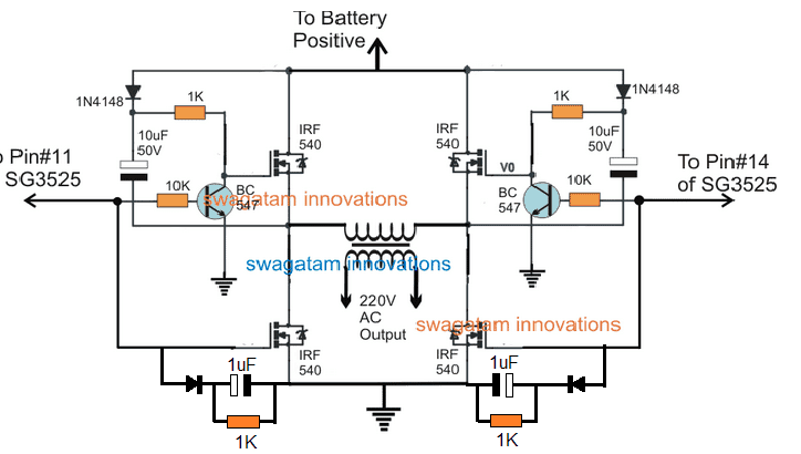
Thee following diagram shows how a dead time could be introduced at the low side mosfet such that whenever the BC547 transistor switches causing the upper mosfet to turn ON, the relevant low side mosfet is turned ON after a slight delay (a couple of ms), thus preventing any sort of possible shoot through.
Using IR2110 half bridge driver ICs
This is basically an SG3525 based full bridge inverter driver, using two IR2110 half bridge driver ICs.
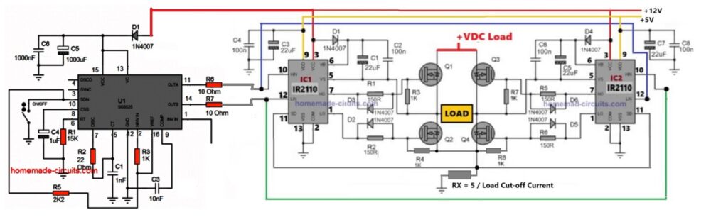
Left side we see SG3525, marked as U1. This is the PWM controller which creates two complementary PWM outputs from pin 11 and pin 14.
R1, R2, C1 around it set the oscillator frequency. If you change them, then frequency shifts accordingly. Pin 8 and pin 9 handle soft start and compensation, so when power comes then it does not slam full duty immediately. The ON/OFF switch goes to SDN pin, so if you press it then PWM shuts down.
This section only makes timing pulses. It does not drive MOSFETs directly, that part comes later.
Now middle section, we have IC1 and IC2, both IR2110. Each one handles one half bridge. Since we need full H-bridge, then two of them are used, so together they form full bridge driver stage.
From SG3525, pin 11 output goes through 10 Ohm resistor to one IR2110 input. Pin 14 goes through another 10 Ohm resistor to second IR2110. These resistors are there to limit input current and reduce ringing, otherwise if edges are sharp then noise can come.
Now bootstrap part, this is important. For each IR2110, D1 which is 1N4007 plus 22uF capacitor form bootstrap supply. When low side turns ON then capacitor charges, and when high side needs to turn ON then it lifts the gate above +VDC Load.
Without bootstrap, high-side N-channel MOSFET will not turn ON properly, since gate must go higher than source, so then it fails.
Right side is power stage, full bridge using Q1, Q2, Q3, Q4. Top left Q1, bottom left Q2. Top right Q3, bottom right Q4. Load is connected between midpoints of the two half bridges.
When Q1 and Q4 turn ON then current flows one direction through Load. When Q2 and Q3 turn ON then current flows opposite direction. So now alternating happens, therefore AC appears across the Load.
Gate area we see 150R resistors, these are gate resistors, they control gate charging speed. 1N4007 diodes help discharge gate faster or protect if reverse condition comes. 1K resistors are pull-downs, so if driver is inactive then MOSFET stays OFF, otherwise it may float and turn ON randomly.
Supply rails now, top red line is +12V. Yellow line is +5V logic. Blue line is driver supply. +VDC Load is the main high voltage DC bus feeding bridge, for example 160V or 310V depending on design. If DC bus increases then output AC amplitude increases accordingly.
At bottom there is RX = 5 / Load Cut-off Current. This is current sense resistor. Voltage across RX goes back to SG3525 current sense pin. If load current exceeds set value then voltage rises across RX, then SG3525 detects it and shuts down PWM. So protection is there, not open loop blind system.
That is the whole circuit operation, from PWM creation, to driver boosting, to MOSFET switching, to AC across Load, simple but solid.
An Easier Full Bridge Inverter using P-Channel MOSFET
If you think the above SG3525 full bridge inverter circuit using 4 N-channel MOSFETs is too complex for you to handle, then you can rather try the following simpler design.
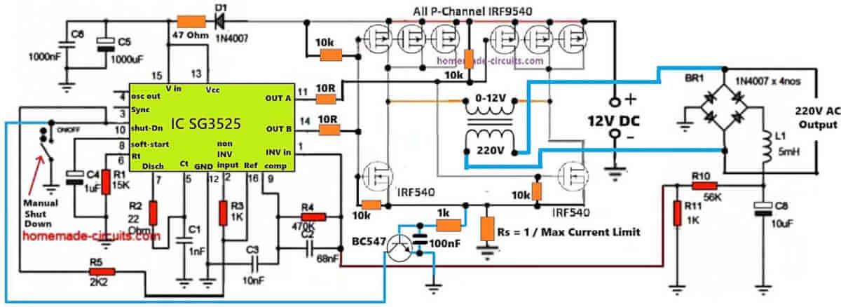
It replaces the high side N-channel MOSFETs with P-channel MOSFETs, thus eliminating the need of a bootstrapping network.
You can see 3 to 4 P-channel MOSFETs are connected in parallel on the high side, while only single MOSFETs are used on the low side.
This is because P-channel MOSFETs have relatively higher RDSON resistance specifications compared to the N-channel MOSFETs, which have very low RDSON resistance.
To make sure the P-Channel MOSFET's RDSON resistance matches with the N-channel counterpart, more number of P-channel MOSFETs are connected in parallel, which makes sense.


Questions & Answers
Can you make a 120V AC version, I’m in USA bro!
Sure Bro, just use a transformer with secondary side rated at 120V AC, that’s all…
Hello Swagatam, I trust your day is fine. I want to verify something please which is related to the question you have already answered. choosing a bootstrap capacitor is really a challenge please could you give us a detailed and general formula to calculate that which can be used for 12v, 24v 48v e.t.c of inverters. for 12v inverter for example, as you have above, base on the rule of thump the bootstrap capacitor should be at least 10x the supply voltage, here are we to consider the voltage of the capacitor or its value to be 10x the supply voltage. in the diagram you used 10uf, 50v for the bootstrap for a 12v inverter
Hello Moses, If you want to calculate the boostrapping capacitor with accuracy, then you can try the following formula. I am sure of any other easy alternative other than this.
C ≥ 2 * [(2 * Qg) + (Iqbs(max) / f) + Qls + (Icbs(leak) / f)] / (Vcc – Vf – VLS – VMin)
Where:
Qg = Gate charge of high-side FET
f = Frequency of operation
Icbs(leak) = Bootstrap capacitor leakage current
Iqbs(max) = Maximum VBS quiescent current
Vcc = Logic section voltage source
Vf = Forward voltage drop across the bootstrap diode
VLS = Voltage drop across the low-side FET or load
VMin = Minimum voltage between VB and VS
Qls = Level shift charge required per cycle (typically 5 nC for 500 V/600 V MGDs and 20 nC for 1200 V MGDs)
Capacitor Voltage Rating:
The bootstrap capacitor voltage rating should be at least 3 to 4 times the supply voltage to have proper reliability.
For a 12V inverter you can use a 50V rated capacitor (common choice may be: 10µF, 50V).
For a 24V inverter you use at least a 100V capacitor.
For a 48V inverter you use at least a 160V capacitor.
Capacitor Value (μF):
A general rule of thumb is to use a bootstraapping cap which is 10 times the gate charge (Qg) of the MOSFET.
For low-power inverters (like 12V, 24V, 48V systems) a 10µF is a good choice.
For higher power, you may need 15µF or 22µF to ensure enough charge.
Hi sir I have an ADH refrigerator rated 220V AC and 0.8A
Can u design for me an inverter circuit to run this refrigerator because I’ve tried my best and failed to make one. Thanks
Hi Joseph, can you please tell me which inverter design did you try, with full specifications, and what issue you are facing? I will try to figure out the problem…
Am using an old transformer without spec but it’s secondary winding size is 10 SWG .The PWM Driver uses IC SG3524 driving into two IRFP150 MOSFETS. So whenever I connect the refrigerator, the voltage drops from 240V to 190V ac and the compressor cannot start. The compressor is not capacitor start type but it uses PTC resistor for starting.
The refrigerator works fine when connect it to grid power supply.
And what is the battery Ah rating? Is the battery voltage also dropping?
Since your refrigerator start up current could be around 400 watts, make sure your inverter is rated at, at least 450 watts.
No the battery only drops from 12.6 to 12.3
Then the battery may not be the issue. In that case it seems the transformer is the culprit and could be having some hidden issue.
Please connect a 200 watt filament bulb as the load and check whether the voltage drops or not, if it drops then certainly the transformer is the culprit.
The battery is 75Ah
Hello, I am in Iran, I have prepared the circuit, but when the consumer is connected to the circuit, the frequency jumps, sometimes it is 40 Hz, sometimes 20 Hz, and sometimes 80 Hz. If I disconnect the consumer, it goes back to 50. What is the problem?!
Hi, is the output 220V dropping when you connect the load? Please check the output AC across load and before connecting the load. Also make sure the 12 supply to the IC is regulated through a 7812 IC and capacitors.
Yes, I prepared the circuit with 4 MOSFET irf740 to convert 220V DC to 220V AC. My oscillator is 50Hz but when I connect to the output of a 100W lamp it goes to 80Hz. If I connect a low-power 10 watt lamp, it reaches 40 Hz. If I don’t connect anything to the output, it is ok at 220 V, 50 Hz. I don’t know where the problem is. I tested 5 different 50Hz oscillator circuits and all of them had the same problem.
Which oscillator circuit have you used, and how are you supplying the DC to the IC?
Hallo Mr Swagatam.I have challenge for you.Please advice , how is possible prepare H bridge mosfet , 50 to 100kHz PWM, to convert 300V ( rectified 230V ) for about , 900-1300V , 1 A (anodes), 250V ,100mA (2grid) , 12.6V ,12A (ad filament ), -80 V( 1 grid , BIAS ) , 800 to 1000W total power. I need to change , my 100 kg charger use for 1kW HF PA ( 2 x russian tubes ) for nice and small PWM supply.But this is some difficult for me.Is this possible ?Please help me , becouse am very impressive.Gregory SP9CNN ,Poland
Hello Gregory,
For the full bridge circuit you can use the first concept from the following article:
https://www.homemade-circuits.com/simplest-full-bridge-inverter-circuit/
For getting different voltage outputs you will have to incorporate a transformer with separate secondary windings for all those outputs. A transformer designer will be able to help you out in this regard.
Hi, good morning. I made the inverter, it worked for some time and stopped. I even had to make more boards but all ended up same way. what should I do?
Please check what went wrong, check the MOSFETs, and the IC an,d try to find out what is blowing…I will try to figure out the cause…
good day, I made the inverter as seen but there was a ticking sound in the mosfet side, how do I get rid of the sound please
Hillary, It is difficult to say the reason of the ticking sound without practically seeing your circuit. Is there anything heating up?
there is nothing heating up at all. I had to make a separate set of MOSFET, but same thing happened
Please remove, or disconnect the transformer and check again…
Hello Mr. swag, i have a 2.5kva inverter I built using your first diagram design, bit I would like to replace the bc547 transistor with a Darlington transistor like tip122 to help improve on the gate current to be able to withstand more load. Do you think it’s necessary, if it is, how do I integrate the tip122 in the circuit (with it’s base resistor)?. Thanks slot
Hi Chinomso,
The load is handled only by the MOSFETs, so upgrading the BC547 is not necessary.
thank you swagatam for your quick response. I am curious not to blow the high side fet- I build one already but the capacitor is 47uf 50v and can 35uf 100v be used?
Moses, actually I have not yet tested the design, i got this from one of the online forums, yes 35uf 100v should be good according to me.
Good day mr Swagatam, how is work and the family? I want to verify something: in choosing the right capacitor for a bootstrap network, is the voltage of the capacitor more important than its capacitance or the capacitance should be considered first. For example what should I consider first when choosing the right capacitor for 24vdd supply for full bridge inverter?
Thank you Moses, everything is good so far.
The capacitance value is more important, which can be anywhere between 10uF and 22uF.
For 24V Vcc, the capacitor voltage rating can be around 50V, as per the standard norms.
pls can I connect a 22k across the gate and source of only the low side MOSFET and eliminate the high side since the high side has a switching transistor 547. or should I connect it all because for the high side the source is connected to drain of low side so am getting it confused on how to connect it on the high side MOSFET since it has a 547 with the MOSFET pls.
You are right, the a gate/source resistor might not be relevant to the high side MOSFETs due to the presence of the bc5477 transistor, therefore you can use the resistor only for the low side MOSFETs…
Sorry Mr. Swag for asking much. I forgot to state that my oscillator IC is sg3524, does the signal matter here?
It doesn’t matter, because the basic working of both these ICs are identical.
Hi Mr. Swag,
I built a full bridge inverter using your above explained design. However, I made use of irf3205 MOSFETs in parallel since I intend to drive the winding on 5000watts automatic voltage regulator transformer. I also used 100uf capacitor for the high side. The issue is that, the system works fine on a low low current battery input, such as 12v 14a source, but burns the whole MOSFETs on a 12v 200a battery source. Could the problem have come from the transformer our 100uf capacitor?. Also how could the high side capacitor be measured to attain smooth switching?.What do I need to improve on to make this work well?. Thanks
Hi Chinomso,
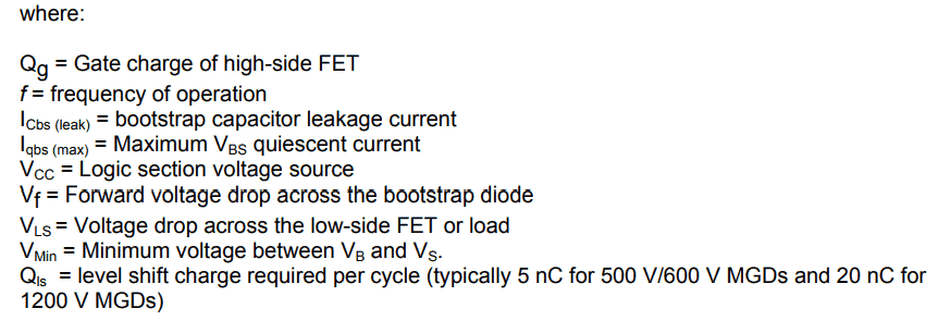
Calculating the high side bootstrapping capacitor can be quite complex, here’s the actual formula to calculate it:
However, normally this value can be anywhere between 10uF and 22uF.
To prevent the MOSFETs from burning you could try a few things.
1) Check whether the current drawn by the transformer is too high or not.
2) Implement soft-start for the IC SG3525 so that the MOSFETs are not subjected to sudden current inrush.
3) Add a 10k resistor across gate/source terminals of all the 4 MOSFETTs.
4) Add reverse protection diode across the drain/source terminals of all the 4 MOSFFETs
Let me know if that helps.
How can this h-bridge circuit be powered with a 24v battery is their any changes with the boost capacitor, diodes and dead time value
You can disconnect the anodes of the 1N4148 diodes and feed a 12V to these anodes through a 7812 IC, and supply the 24V only to the drains of the High side MOSFETs.
So this setup works well even though the transformer isn’t a center tap one
It is a Full bridge inverter circuit so center tap transformer is not required here.
Hi Mr Swagatam,
I’ve built a 1.5kva inverter with the Hbridge system and it working well, and in reverse, I could charge my battery from the mains. But here’s the thing; the charging is not effective, especially when the mains voltage goes lower. I would like to install a feedback using an optocoupler, please do help me out in this, as a diagram would be more helpful. Thank you so much in anticipation
Hi Chinomso,
You asked this question earlier and I have already answered you, please check your email for the link, it might have gone into your junk mail..
Hello, Iam aiming to design a circuit to invert 18V DC input to AC output at high frequencies such as 50KHz in order to transmit it wirelessly then re convert into DC at the receiver to charge a battery, how can I increase or decrease the frequency using the topology you introduced if possible. Thanks in advance
Hello, your concept is not feasible, battery charging requires high current which is not feasible using wireless transmission.
Yes I understand but I will be having a very small prototype for university it will not require actual charging I just need to transmit any sort of power.
Wireless electricity transmision may be possible only for a short distance of a few inches or a foot. As the distance increases the efficiency decreases. What distance are you looking for?
Yes I have a maximum distance of 25 cm no more.
In that case you can use the search box at the top and search for wireless phone and wireless LED
Hi Swagatam,
May I know the output frequency and wave form of this project. Is it 60hz out put and pure sinewave?
Thank you.
Hi Jack, the output frequency can be adjusted by suitably adjusting the R7, C12 values in the following diagram:

Output will be a square wave
Thank you so much for swift reply.
I must again recommend your good works Mr swag, thanks a lot. my question is, can this circuit work for microcontroller inverters?
Thank you Hillary,
I am not sure how the above circuit can be used with a microcontroller inverter. I will try to investigate and let you know.
Which side is the high side and do I connect the feed back
The top side mosfets are high side mosfets. Feedback can be connected on pin#10 of the IC, by disconnecting it from ground and then configuring it with a bridge rectifier and resistive divider network.
From which pin of the SG3525 can I connect the feed back sir
You can use pin#1 for the feedback control, as indicated in the following diagram:
How can this H-bridge be done using ir2110 driver ic with sg3525
hi sir,
i want to try full bidge induction heater with sg3525 ic to drive igbt with help of 316j can you help me about it.
is this safe or not for igbt .
Hi Hiren,
I do not have an SG3525 based induction heater circuit, but I have a different IGBT based circuit which you can refer in the following article:
Induction Heater Circuit Using IGBT (Tested)
hi sir can you chechk the circuit. its not working.
Hi Celal, I checked the full bridge diagram which you sent me, but it will never work because it uses 4 N channel mosfet without a bootstrapping network.
How I can I do it. I don’t know. may you help me with it because I did a lot of circuits like this and non of them worked. If you can help me I’ll be so glad.
The full bridge is already explained in the above article which you can try. Or you can refer to the following article:
Simplest Full Bridge Inverter Circuit
I want to drive 1000w DC motor in the place of transformer in any way with n-channel MOSFETs to drive pwm with DIR ,please help me,and thanks,with my expects
You can try the following concepts:
https://www.homemade-circuits.com/simplest-full-bridge-inverter-circuit/
Thanks for good job ,send send to me please,not very difficult principal circuit ,,,full H-bridge with 4N- channel MOSFETs to drive 1000watts DC motor,and thank you at all,with my expect.
Thank you, the above explained circuit is very easy to build…
Can this work for the sinewave inverter explained earlier?
It can be converted to sine wave by chopping the low side mosfets with SPWM
Thank you very much
So what can we use to replace that transformerand still performer the same function….
So what can we use to replace that transformer?
And I couldn’t find this IC SG3525 on Proteus library ….pls how can I get it
You will have to use the following concept:
https://www.homemade-circuits.com/how-to-convert-3-phase-ac-to-single/
sorry I don’t use softwares so can’t help with proteus issue.
pls i need a circuit diagram design on transformer less automatics voltage regulator.
that is the project am working on and I’m facing some difficulties on it
Sorry, I don’t have this design with me right now.
if we dosnt want to use that transformer what else can we use to replace it and still get 220v at output.
and this IC component is found in proteus for simulation where can we get it
without transformer you cannot get 220V from 12V
Okay….what if we generate 214v from bridge rectifier and use it as an input to the H BRIDGE circuit, instead of 12v…so is it possible to get stable 220 output without transformer
Yes that’s possible but the output will turn into a square wave
dear Swagatam; I redrawn the circuit and succeeded. but as a result of many trials, I found the most ideal values on the circuit by experimenting. I use 100uf instead of 10uf. Instead of 1k, I use 2.2k, 1w or 2w mosfets (irf840), even without cooling. It works for 8 hours, the temperature is super (21khz)
That’s great Mesut, I am glad you could improve the H-bridge design with some modifications in the part values. If possible please provide the drawing through an external link.
Thank you sir I’m reading your ideas but are so teaching and valuable,infact am going to like site , becoz I love electronics
Thank you Kintu, I appreciate your thoughts!
Hello sir swagatam
I’m very interested in one of the inverter welding mention diagram that you shared but some parts of it like L1and L2 is being closed please can I get the direction on how to connect it.
Hello Samson, please post your question under the article you are referring to.
Hi Swagatam,
I am very grateful for all the information you have provided me. I have build a lot of your projects. So thanx for that. Just one question. The circuit mentioned in this site (which i love) i have build and even added more mosfets with great success. My question : i want to convert this 12v project to 24 or even 48 volts. What i don’t understand is whats the point of putting on a 24v battery and then just adding say a 7812 to protect the ic or adding a dc to dc step down converter. At the end of the day everything just comes back down to 12v.
Am i missing something or can you help by upgrading this particular circuit to 24v. i Don’t want a center tap circuit as your full H-bridge is much more efficient to me.
Thanx very much for always answering my questions.
Regards
Peter
dear peter I converted this h bridge to pcb but it didn’t work. Can you share how you did it?
Thank you Peter, Glad you found the projects helpful. 12V or any lower level voltage is suggested to safeguard the IC since most ICs are not built to handle 24V or 48V. Such ICs are only used as an oscillator source for feeding the mosfet or BJTs. The actual 24V or 48V is used with the transformer and power devices to boost the power in that order.
Higher voltage at the output stage ensures proportionately lower current, which in turn means cooler transistors, and more compact inverter size….comparatively for lower voltages such as 12V units, the current, size and heat dissipation will be much higher.
Thank you for the input
So how do i feed 24v or 48v to the mosfets without damaging the ic. Since i will be using a voltage regulator to step down the voltage for the ic like a 4047 (15v max). so the 4047 outputs wil still be around 6v each which does not solve my problem. I saw a few of your circuits were 24 or 48v was applied but that was with a center tap transformer. i would like to implement higher input voltages to your h-bridge circuit.
Does that make any sense., or am i lost. i don’t wanna compromise the h-bridge for a center tap
If you can show me how my battery connection would look like regarding the above h-bridge circuit i will be grateful.
Thanx again
Peter
The output of 4047 or any similar IC will be almost equal to its supply voltage, So if you are using 12V for the 4047, its ON time will be almost 12V, which is sufficient for the MOSFETs.
In the above h bridge, you can isolate the diode anodes and connect them with the 12V, and connect only the drains with the 24V or 48V battery.
Before this make sure to test the full bridge with 12V first, just to confirm its working.
dear friend.Swagatam why?h bridge 2pcs p channel mosfets 2 n channel mosfets are not made cross way.I’m reviewing all the circuits. But no complete result was found.
Hello Mesut, using 4 n channel is the most efficient method of implementing a full bridge circuit, you can use n channel and p channel also by appropriately matching their RDson values.
Thanks for the quick response. I have now researched (RDS ON) it is very different. I’m working on wireless energy. My goal is to run at 20khz. I succeeded with 2 mosfets. I want to try the h bridge to develop it. That’s why I’m doing research. can you update the h-bridge picture..sorry for the english.
For p channel and n channel bridge circuit, you can try the following topology:
I’m irf9640 and irf630 rds very close what is your opinion. I’m very undecided h bridge pcb did not happen.
Anyone running this h bridge circuit?
because i prepared pcb but it didn’t work. The circuit is not working. Do you have a trial drawing?
thanks for the answer. I made a h bridge drawing pcb, but it didn’t work. 1 mosfet is getting hot. There is no heat for the mosfets.
The concept used in the bridge network is correct you can verify it from anybody, however I have not tested it myself, the idea was taken from one of the forum discussions.
If you are having difficulty with the above design you can try a simple p-chanel N-channel mosfet bridge.
Hi, I do repair inverters with center tap transformers but most of the transformers now a days is no more center tap so I will like you to give me a circuit using sg3524n on how to drive the transformers without center tap
Hi, It is already explained in the above article.
From SG3525 full Bridge inverter diagram, I built it, it was OK but can’t charge.
What should I do to make it charge batteries?
There are many charger circuits explained in this blog, you can use any one of them to charge your battery
I tried using SG3524, but my sg got blown up. So what should I do?
Thanks
The transformers when I plugged them into light , 12v input battery reads 6v, 24v input battery reads 12v.
So my question is if I put in the circuit you gave me, will it charge?
Which circuit are you referring to….?
Can this H-Bridge topology be adapted to work from high voltage rail (rectified 220v ac)?
I can see a bootstrap challenge. Perhaps you will be kind enough for another version?
It looks difficult to implement high voltage in the proposed circuit, you may have to employ a specialized full bridge IC for that!
Please I built this full bridge inverter using sg3525 with this circuit this is what I’m observing if I test the oscillator board every is working fine and I have 50hz but when ever I link the oscillator board to my MOSFETs that’s the switching unit the frequency changes and keep fluctuating to different frequency and if I link the transformer to it, it will burn the MOSFET please what could be the possible cause to this
Please use an oscilloscope to test the frequency, duty cycle etc, DMM can give misleading results.
Actually I did test with my mini oscilloscope it give accurate value of 50hz and the wave form is correct but when ever I connect transformer to it, it will bow up my MOSFET so I was confused which one to believe oscilloscope or DMM
Scope is correct, DMM is not. Try increasing the dead time, an try implementing all that’s mentioned in the following article:
How to Protect MOSFETs – Basics Explained
Hello Mr. Swagatam.
Greetings sir.
Please I have an issue that borders me so much. I made a 5.5KVA inverter which is being used to power a 2.5KVA SUMO (water pump), a deep freezer of 0.7kw, and other lighting points, and FAN, TVs in the house. But the problem is that each time the whole appliances are powered at once, the output filter capacitor blows and this also burns the whole MOSFET in the inverter. I have used 104, 400V in parallel with 225, 400V X rated capacitor to filter the output and it burns, I replaced the with 2.2uf, 275 MKP capacitor and it lasted for about 5 days and the same problem occurs again.
Please help rescue me from such trouble. what value of filter capacitor will I use for a 5.5KVA inverter? Or is it appropriate to remove the filter entirely (i.e do away with the output filter)?
Hello Kingsley,
Good quality capacitors should never blow, especially when they are correctly rated. Try using 630V metallized polyester type capacitors and check the response again.
Pls I need a link explaining parts or section and working principles of the sections.
Example drivers part, buffer part, etc
Last day example if inverter is working but not charging battery, check this part.
Thanks
Obviously a bomb. Pls practice your circuitry before publicising it. Mere looking at the IN4148 with 1k resistor connected to the gate of ir540, you will simply understand that the ir540 drain to source is constantly closed with Direct current. Dis will blow up the fets
Don’t worry nothing will blow up here, you merely looked at the diode/resistor but failed to notice that the input to the BC547 base are alternatively switching, which means vertical MOSFETs can never be ON at any instant, so the MOSFETs can never burn….Now I hope you have understood that the circuit is fine to use….
Hi, Sir
Thank you very much for the H-bridge circuit diagram. Its much more efficient than the center tap circuit.
My question is, do you have a circuit diagram for a bigger inverter, by that i mean something with more watts output. I used to same 12v-0v 6amp tranformers in parrellel but that only helped to share the load.
Thank you
Peter Ferreira
Thanks Peter,
For bigger transformers you just have to upgrade the MOSFET and the battery power rating appropriately.
Hello swagatan, am very happy for the good work you’re doing for us here, my question is, what if am using a microcontroller and not sg3525
Secondly, does the above network works similar with IR2110.?
Thank you Wilson, any flip-flop oscillator can be used as the input source, and it should work. You can use a microcontroller based oscillator, IC 4047, BJT astable, or any similar all should give the intended results, just make sure to add an appropriate deadtime
Dear Swagatam,
SG3525 Full Bridge Inverter Circuit
I have studied the circuit with great interest, as I am wanting to produce a 1kW design using the SG3525.
Having been out of the electronics industry for many years, my memory and knowledge is being stretched to the extreme !
I can follow the description given generally, however, would appreciate your help in understanding what the discharge path for the capacitor is ( referred to in item 7)
7) During this situation the capacitor is forced to discharge quickly and the mosfet is able to
conduct only for so long the stored charge of this capacitor is able to sustain.
As I see it, the FET has a High gate impedance, so the discharge cannot be via. the gate / source junction, so I am a little confused.
Also, the 10uF capacitor and 1k resistor give around 7mS time constant, which seems very excessive, as the system is operating with a PWM frequency of 114kHz (according to data sheet and components shown) giving 57kHz transformer frequency – surely the capacitor would only need to hold the charge for 1/2 cycle (just under 10 uS).
As a side issue, I also want to run from a 60 volt battery pack to keep the current reasonable, as I will have 4 x floating 1kW units running together, feeding a 4kW grid tie inverter. 60 volt rail will result in the gate-source voltage being exceeded on the upper FET’s, so plan to use two back to back 15v zeners to clamp the gate – source within the 20v limit.
I am obviously misunderstanding the situation somewhere with the bootstrap circuit and would appreciate some help prior to committing to the build and risking components !
(Sorry for the long text)
Peter
Dear Peter, the capacitor discharges when the BC547 and the low side MOSFETs are switched ON, in this situation the capacitor leads are shorted with only the 1k resistor in the path.
The 10uF is not a calculated value and will need to be optimized by the user as per their preference, nevertheless it is intended for a 50 Hz frequency. The SG3525 circuit is only for reference purpose and its components will need to be adjusted for getting 50 Hz output.
For more info regarding the bootstrapping you can go through the following article:
https://www.homemade-circuits.com/h-bridge-bootstrapping/
Hi Swagatam,
Thank you so much for the rapid response and answer, which has clarified things – very much appreciated.
Peter
You are welcome Peter!
I have 24v, 220v hbridge type transformer ( without center tapping). which of your circuit can use for making an inverter by using the above transformer and also as a spwm?
If i input 330VDC at load voltage,will I have output as AC without using transformer on the load side?
Yes that’s correct.
swagatam , ıf I Show the my pcb schematic , Could you look after about okey or not ?
But for the send schematic ı need your email .
gulay, verifying PCB design can be time consuming, so it may be difficult for me to do this for you due to lack of time…
Swagatam ,
I design full bridge single phase inverter closed loop , Share with the formulas with me ?
I can not determined the frequency , Load R and Load L . Please help me ?
Thank youu 🙂
Sorry, I do not have the fomulas, whatever details I had I have presented it in the above article.
Hı Swathagam
SG3535 is make the closed loop otomatically , One of the feet is feedback . Am I wrong ?
Thank you 🙂
Hi Gulay, you can refer to the 3rd circuit from the following article, and learn how to add a feedback loop to the circuit
https://www.homemade-circuits.com/sg3525-pure-sinewave-inverter-circuit/
Hi Swagatam ,
I want to obtain square wave singe phase full bridge closed loop inverter . Which PWM producer am I used ?
And Share the schematics with me.
Thank you,
Hi Gulay, the required circuit is already given in the above article. You can apply the last schematic for the full bridge stage, and integrate it with any SG3525 oscillator module. However, for a closed loop you will have to add a feedback circuit as shown in the following diagram:
Hi , these are half bridge (2 trasnsistor)
How is the full bridge single phase inverter with sg3525 ?
Please , Answer my question.
If you have an oscilloscope troubleshooting will be easier, check the output waveform, if both pin 11 and PIN 14 comes the same time i.e when one if on the other is off the same time and there is no delay before the the next then that is the problem
hello Sir, I am from Argentina, I am trying to make the full bridge inverter for a solar system. But I used igbts 30j124 instead if the mosfets and the capacitors in the bootstrap are 35v, I cant find here 50v 10microF.
I proved with a lamp and works great, I tested with a tester and the voltage in Ac and is 30v and the frecuency is 49hz. But yesterday when I try it with the transformer, two ijbts burned. Do you think I need some protection for the igbts? maybe a diode in paralell?
Hi Luis, if it’s happening with a transformer only then it could be due to back emf spikes. You must connect reverse diodes across collector/emitter of the IGBt, and also connect a 100uF capacitor across the positive/negative supply rails of the bridge.
Thank You Swagatam!! for taking the time to reply to me. This circuit it’s of great help to my family, we will take a warm shower with this!!
You are most welcome Luis, please keep up the good work!
Sir swagatam,do you mind updating the sg3525 full bridge system for me for a 24v dc supply,iam about to start the process of construction of the 6000w/24v inverter,I have already consolidated the requirements but I don’t want to messing any way. Please I will be
happy if you could update this full bridge
https://www.homemade-circuits.com/sg3525-full-bridge-inverter-circuit/?unapproved=74295&moderation-hash=12568f8795f12b87d88e0b2268189fb5#comment-74295
https://www.homemade-circuits.com/sg3525-full-bridge-inverter-circuit/?unapproved=74295&moderation-hash=12568f8795f12b87d88e0b2268189fb5#comment-74295
Evans, the above design uses discrete components which means a slight mistake will blow the MOSFETs. Since you are a newcomer you must go for the specialized full bridge ICs…But anyway none of the full bridge designs are recommended for newcomers.
You must first start with smaller designs, and then gradually as you learn you can upgrade them for more power output. Look for the specilaized ICs, if you don’t get them then make the center tap version.
Ok sir,but I have been making square wave ones with centre tap for quite a long time now,so wanted to upgrade hence thought you could be of help.
center tap may be bigger in size but will give you fail proof results, full bridge may not.
Sir swagatam,is there any difference between sg3525 and sg3524?
SG3525 is an improved version of SG3524, but the basic functions are identical.
Ok sir,can I use the ic 4047 circuit that you provided in your earlier articles and integrate spwm with opamp? Will there be any modifications?
yes you can try that using P channel and N channel mosfets, but with adequate precautions that I mentioned earlier
Sir I noticed that there’s no voltage at the negative of the 10uf and when I connect the driver to the mosfet voltage drops drastically also the mosfet heat up very fast, is like it shorting
Good afternoon sir, I’m having a serious challenge, I build a hbridge and I build the boostrapimg drive the hbrigd while sg3524 is use to drive the boostrap for but when ever I power it my mosfet blown or at times the voltage will drop to the extent that there will be no output from the ocillator board, but if I power the oscillator board alone it works fine. Please what could be the cause
Faith, short circuit can happen only when the MOSFETs in the same vertical line conduct together, which cannot be possible in this configuration. The BC547 will never allow both the vertical MOSFETs to turn ON together. Make sure your IC is working correctly, and has some dead time set.
Always Test with 12V car head light bulbs in series with the drain pin of the MOSFETs
Sir please I want to ask what could cause the output of the se3524 fluctuating because I noticed if I put the sd3524 my regulator will heat up but if remove it the regulator will not heat up again I noticed the output of the ic is not steady what could be the cause
Faith, did you add the L2, C16, C17, D3 as shown in the second diagram? Try replacing the L2 with a 220 ohm resistor and check the response
I only add 1000uf,25v, but will that cause Both on and off time to happen the same time, because, Sir this is not my first time of building this the first and second time I build this it works fine but I don’t know what is wrong with this very one, now I took my time to troubleshoot it but I couldn’t fine any error I now check the output waveform from pin 11 and 14 and I observed that both on and off happen the same time, which is not supposed to be so, now I compared it with the old board I have and I observed that in the old board there is a delay between the on and off time, what I can’t figure out is why is Both on and off time happen the same time, which I believe is the cause of my burn mosfet, please sir any ideas why this is happening
Sir swagatam,so if I use a 4047 oscillator to the updated full bridge network you have provided with the dead time,will the outcome be same as if I could have used sg3525? Or should add/subtract anything? Again sir how will the direction of the 3v zener diode? Where will the anode and cathode connect?
No changes will be required because the output of the two ICs work in a similar fashion…
Hello sir swagatam,can you send me the diagram for 4047 you are proposing for faith to use? Am facing the same issue with sg3525. What am wondering is will 4047 feed to he full bridge without any modifications?
Evans, SG3525 is a precision IC, and will never produce wrong output unless the connections are wrong the IC itself is faulty. Yes you can connect the 4047 output with the specified full bridge network.
Hi Faith,I seem to be facing similar issue, please would you mind sending your diagram on how you trouble shoot the problem I will really appreciate
Sir I have rectify the problem and is working fine now thank you so much for your help I’m really great full,
Glad you could solve it Faith…keep up the good work!
The output should work in push-pull manner, when one pin is OFF the other should be ON and vice versa. Use 4047 IC instead if you are finding it difficult to handle.
Also why it’s that the connection of a Zener diode in series to the base or gate of a transistor is important and why being specific at the voltage rate of 3V please sir I need more light on this
Thanks and may The Lord god continue to blessed you for the good work
As explained in the article, the 3V zener will keep the MOSFETs OFF until a genuine trigger above 3V or upto 12V appears at the gate of the MOSFET. This ensures that the MOSFET switching across the two channel is isolated by a minimum 3V value, and they never conduct together due to minor stray leakages
Hi swagatam please can this circuit be modified by adding the PWM circuitry or SPWM circuitry and which side of the MOSFET is high/low also why it’s that when modifying a circuit the PWM or SPWM circuitry is always being connected to the low side of the MOSFET not the high side of the MOSFET thanks
Hi Emmanuel, yes it can be controlled with SPWM on the low side mosfets. PWM integration with low side mosfet is implemented only on full bridge topology which uses 4 MOSFETs and no center tap transformer.
Hi,tanx for Ur helps.before now I ve had successes with this cct,but now am having problems.for a 12volt inverter, if battery voltage is 12.5volts, the transformer makes noise until the voltage drops to about 11.0volts,then the noise will stop and inverter works well.
Sir,what can I do as a remedy,i ve been using this cct for two years now with great success.
Thanks Charles, did you use any kind of feedback or some other customization? I would suggest to test the inverter in its basic mode and see if the problems still exists.
Thanks a million 4 Ur time.if used with a centertap transformer,it wok’s very well,hwever full bridge inverters are more economical.am presently working on a new design, I will update you later. Thanks.
Sure, thanks for the feedback!
Thank you Swagatam sir.
You are welcome Manuel
Dear Swagatam sir,
Doubt cleared sir, thank you for your immediate response. Matching Transistor MOSFET for 200w inverter ?
You are welcome Manuel, the MOSfeT can be IRF540
Dear Swagatam Sir,
I am late comer in your tutorial regarding Inverter Circuits. I am about to make one by your instruction, Sir generally which type of transformer we can use all these circuits,I mean normal 230V AC to 12-0-12 step down Transformer we can use by Reversing the Sec. side to (12-0-12) as Input ? My requirement is approx 200W.
Welcome Aboard, Manuel. Yes that’s right, you can any use normal step-down transformer as a step up inverter transformer just by turning it the opposite way.
Step-up or step-down conditions depend on which side is being used as the input and which side as the output
his sir can u plz make a code in arduino uno which generates 3 positive and 3 negative pulses for igbt gate driver circuit…
Hi Ahmed, I am not good with Arduino so coding can be difficult, but this can be perhaps implemented using external totem pole transistors also
Hi Swagatum
Hello Robin!
Hope you are well
Just out of interest
Refering to the above circuit I tested it on my oscilloscope awhile back and found that there was some shoot-thru because of the inversion of the signal,so i tried these two circuits which work perfectly.I also built a similar circuit with the dedicated high low side drivers(IR2110) which still outperformed these.(trying to send you some images)
I plan to try the second circuit where you have introduced the dead time for the low side mosfets and check the results
Juust in case can i still send an email to: hitman2008 @ live.in
Hello sir… Rply me sir i have no much more time… Please help me for making this project….
Hello Apurva, I have just changed my website URL so your previous comments might be deleted. sorry about that!
I have already answered to all your previous questions. Please let me know if you any further doubts.
I made that full bridge circuit and I used atransformer which had 12v at its at its primary and 220v at its secondary and it inverted igot the out put voltage 220v but when I load my inverter the output drops to 170v but may inverter need feedback at the ic can you help me with that feed back circuit sweetable for that sg 3525 ic circuit
You can add a feedback to pin#1 of the IC as shown in this diagram
Hi, can this bootstrap circuit work at high frequency like 100khz, I require it to operate ferrite core transformer??
yes that’s possible, just make sure the ferrite trafo is correctly matched with the frequency and the voltage
Will the transistor BC547 respond at that high frequency of 100khz??
yes it should, BC547 is rated at 1MHz
Thank you so much for helping, one last question, how many MOSFETs can I connect in parallel? for bc547 to be able to drive them? Or can u suggest me more powerful transistor for bc547, or can I use IGBT’s
Thank you so much again
You are welcome!!
Rohan, mosfets and IGBTs require minimal current at their gate/base to operate, therefore no special BJTs are required, BC547 can be easily used
Hi Engr Swagatam. Pls, where do I connect pin #10 of IC 2535 for shut down against overloading etc.
Hi Yusuf, you can connect pin#10 with the output of the following opamp circuit.
https://www.homemade-circuits.com/automatic-output-voltage-regulator/
eliminate the transistor stage completely and connect pin#6 of the opamp directly with the pin#10 of the SG3525.
Make sure to use 3 or 4 1N4148 diodes in series so that the opamp output leakage offset voltage is blocked.
sorry, the said arrangement will prevent over voltage not overloading, to control overloading you may have to swap the input pin numbers of the opamp, meaning pin#2 and pin#3 must be swapped, and the recommended output diodes reversed
hi sir,
S1 S3
| |
——– TR ———
| |
S2 S4
is there any deadtime between high (S1) and low side (S2) mosfet? since there are came from 1 source (Pin11 SSG3525)
i think would be better if add some deadtime at the moment they are switching to prevent 1 side are not fully off but another side is aready on.
thanks.
Hi Rudi, yes dead time can be set by adjusting the resistor at pin#7
https://www.homemade-circuits.com/understanding-sg3525-ic-pin-outs/
hi sir,
sorry sir, i think you get me wrong. i know pin7 is to adjust deadtime between outpin11 and outpin14. but what i means is between low and high side of fet. since they are opposite, for example, if pin11 is high then the low side would be high too, but at the same time high side will turn low., if we operate at some high freq, is it possible the low side is go high while the high side of fet are not fully turn off?
i think would be better to have some deadtime between them for keep it safe. i know low and high fet (at the same side) cannot be turn on together, this will blow up the fet.
thanks,
Hi Rudi, you mean to say during dead time since the BC547 BJTs would be OFF, the high side mosfets would be turned ON, you want to have all the mosfets turned OFF during the dead time, right? I am sorry that looks difficult for this particular design.
To satisfy this condition you may have to try a full bridge topology using p and n channel mosfets as shown in the following article:
https://www.homemade-circuits.com/arduino-full-bridge-h-bridge-sinewave-inverter-circuit/
Hi sir,
Yes sir. During the bc547 turn off the high side gate to gnd is cut off and make it on by a cap (bootstrap). My idea is at right before that happening, it is better to let the low side off for a short of time to keep the things smooth.
I have read a lot of example on internet, there is one of many ways is to introduce a rcd (resistor,cap,diode) can achive that. But i dont know how to implement it into ur circuit.
Thanks,
Ok thks for the advices. I will try it again when i am got free.
Regards,
Rudi
Hi sir,
I have tested your circuit. When operatr at low freq says 50hz, the waveform look great, prefect square wave. But if i ran at some khz speed, let say 33khz my waveform is very distorted. Its more look like a banana shape.
Can you point me what cause this problem? How can i make this just look as great as 50hz?
Thanks
Thanks Rudi, Glad you could test it successfully.
When you use high frequency, inductive spikes starts getting more active and these spikes could start developing across connecting wires, tracks, solder fluxes, or any other possible unwanted source creating harmonics and distortions.
I would advise you to use a well designed PCB and make the tracks as short as possible across the mosfets and the transformer. The transformer here will be obviously a ferrite based transformer.
also use suppressing capacitors across various nodes as suggested in the following article
https://www.homemade-circuits.com/mosfet-protection-basics-explained-is/
Ok thanks sir
Hi Rudi,
I have updated the required design at the bottom of the article please check it out and let me know if you have any doubts.
Hello Sir, Thank you for the awesome website. Sorry for the silly question but does the connection between the MOSFETs connect to the 12V side of the transformer as well as the 10uF caps or do they just pass over them?
Thanks Again!!
Dylan
Thanks Dylan, Only the negative side of the capacitor is overlapping a few of the other lines…but it is connected only with the source of the respective mosfets, and nothing else.
I cannot see any other overlapping lines other than the above
Sir can I charge 12V battery with 9V or 11V or 15V transformer? I aaked u what is minimum and maximum volt to charge a 12V battery? Sir I hope now u understand
plz make me understand
Thank u
Mehedi, you are repeating the same question which I have already answered….
Sir I asked about charging volt. what is the minimum and maximum charging volt for 12V-95A battery.
sir u said charging current 10A and charging time 12Hr
but
*Total battery Amp / Charging Amp = charging time*
so that 95/10=9.5Hr, m I right?
Mehedi, I have provided the charging details in the earlier comment, you can refer to it for the details. Your charging period calculation is approximately correct…
Sir I have a 12V 95 Amp Sealed led acid Battery,
now what will be minimum and maximum volt and charging current? for safer charge for long lasting the battery life,
Mehedi, it is standard for all 12V batteries, 14.3V full, and 11V low. Charging current will be around 10 amps for 12 hours
SIR THANK YOU, I hv understood it bt
IRFZ44N( just one on each chanel) total 2.
just 2 IRFZ44N will give out put of 400Wattage!? I m so surprised, I hv no batter idea about MOSFET, thank u sir, I have anoter question, if I use your above Full bridge circuit for 400watage out put then which MOSFET should I use?
Mehedi, since The mosfets are rated to handle that much wattage so they will be able to do it comfortably…pleas note that this is as per my analysis.
you can use the same mosfets for the above inverter also
Sir I hv no perfect decision about it.
that’s why I asked u
I m using 650VA (390W) UPS transformer and 100AH battery(12V)
I want 400Wattage output
now my questions are:-
1. if I use your above Full bridge circuit then how many MOSFET will need to use on each Chanel? and which MOSFET?
2.if I use center tape transformer then how many MOSFET will need to use on each chanel? and which MOSFET?
sir plz make me understand correctly about this
Mehedi, I mean to say that if you have asked regarding the dissipation factor then you should have also asked regarding the VDss, and Id factors of the mosfets because these are more prominent factors than power dissipation..
anyway, power dissipation is the value which shows at what power the device may reach its maximum core temperature without a heatsink. So at 94 watts the device may dissipate temperature which may eb dangerous for the device, and therefore adequate heatsinking must be applied to it to ensure it is able to sustain the specified max level of 55 x 49 = 2695 watts
I hope you have understood it now…
Ok…good point. Charge pumps, bootstrapping, isolated drives and other means of high side N channel mosfet drive techniques. Could you talk a little about them? I have discovered that the H bridge for many ferrite inverters hardly use tlp250, but almost all the iron core transformer h bridge does. Why is that so? Please explain. Thanks.
TLP250 is just an enhanced opto-coupler for ensuring safe switching for the connected mosfets, because mosfets can be highly sensitive and unpredictable devices, especially when the triggering frequency is high.
At lower frequencies the vulnerability is reduced to a great extent and therefore no such special arrangement is required for their switching.
However these cannot be used for the high-side mosfets because the bootstrapping needs to be applied directly to the mosfet gate, so intermediate buffer cannot work here.
ok….I get more enlightened each day by your blog …Thanks. I want to implement a H bridge switching , not unlike the one above. Only I want to use a Microcontroller for the SPWM generation. What kind of drive circuitry can I use? Mostly for the High Side Mosfets? I already successfully generated the high voltage VDc from the dc dc converter. I need to understand more the modalities involved. I got a bunch of IR2110, but unfortunately, they are mostly inferior, and act rather unpredictible. I need an alternative drive pattern. Thanks.
unfortunately there is no better driver alternative than the specialized full-bridge driver ICs, therefore you will have to test and optimize your circuit using only these driver devices…make sure to add a 1K resistor across gate/source leads of the mosfets for better stability
I have taken apart several high frequency inverters, and most of them did not use any special drivers, some did. Others used totem pole for switching the low side, and a sort of charge pump for the high side. I didnt completely understand the full rationale for the charge pump. What is your take?
Thanks.
the charge pump is used for bootstrapping and will be required if no special driver IC is used, you can read regrading bootstrapping in this article:
https://www.homemade-circuits.com/sg3525-full-bridge-inverter-circuit/
bootstrapping raises the hi-side mosfet gate level typically to 12V over its drain level, to enable optimal conduction.
Please send me your email sir. I have several questions I would love to ask you, and wouldn’t want to do it here, as it may be different from the topic. I follow your tutorials, and I have been really enlightened.
Thanks.
Mho, I want our discussions to be visible to all the visitors here so that all can benefit through this, therefore it would be a better to present our discussions here itself, in emails the discussions will remain hidden and will be wasted.
I m using 12V 100AH Battery
sir u said one on each Chanel will be enough. that’s mean I need to use total 2 IRF44N.
but my IRFZ44N(Power Dissipation 94 W)
94+94= 188W
188W switching wattage will be 400W by 650VA(390W) Transformer????
sir I m confused how it possible?
in your previous reply u said that :-
Swag says
“The switching devices must be rated above the transformer rating, if the trafo is 500 watt then the mosfets must be rated at minimum 600 watts.”
in this case now transformer is 390W so switching device (Mosfet) must be rated at minimum 490W,
sir I m so much confused!!!!!!!!!
You are right but then what about the drain/source rating of the mosfet, and the continuous drain current rating of the mosfet which are shown as 55V and 49 amps respectively…..please let me know your opinion about this??
Thank you sir for your valuable Reply.
Sir I am designing an inverter for 400watt full load.
I am using your above Full bridge circuit with SG3524 ic circuit, almost everything done and I am getting out put from transformer.
But I am facing a problem that is, I am unable to chose right mosfet for actual 400Watt out put.
so I need your help to chose right mosfet.
I m using 650VA UPS transformer and
100AH battery
now say me what mosfet is needed for this inverter? and how much mosfet in total?
I have available mosfet in my palce :-
IRF44N
IRF540N
IRF840N
IRF3205
IRF3710
please u help me to use right mosfer for accurate Wattage
Thank u sir
Mehedi, assuming your battery voltage is below 48V, you can use the first one which IRF44Z, just one on each channel will be enough, with adequate heatsinks attached
hello SWAG. thanks for your idea. i tried your circuit using sg3524 ic.
the high side drain voltage is 48v, i replaced bc547 with tip41c.
my bootstrap cap. is 160v 10uF. my mosfets are irfp260n.
the 1N4148 is connected to a 12v supply. when i power on, the circuit works but the high side FETs gets hot after a few minutes without load. what i’m i getting wrong?
should i replace the 12v supply wih 48v?
Hi Nick, The upper mosfet could get hot if the gate voltage reaches higher than its rated gate value, you can try measuring this value by keeping the meter probes across the 10uF capacitor, and momentarily switching ON the trigger across the base of the relevant TIP141 transistor…the reading should not be above 60V, if it is above this value then we may have to think of a different configuration in which the drain voltage could be applied separately and the 12V applied independently yet make sure these two become a part of the 10uF cap.
Hello Swag; thanks for getting back to me so soon. what if i change the 1n4148 to 1N4007 and connect a resistor (say 22k) in parallel with the bootstrap cap? what do you think? i’ll try it and let you know the outcome. thanks again
Sorry Nick, I am unable to simulate the configuration in mind so it would be better to get it checked practically and learn how it behaves…wish you all the best
What is Drain side volt of upper mosfer? ( IRF540)
How can I read drain side volt of any mosfet from it datasheet? plz say me
In IRF540 datasheet we know that :-
Type Designator: IRF540
Type of Transistor: MOSFET
Type of Control Channel: N -Channel
Maximum Power Dissipation (Pd): 150 W
Maximum Drain-Source Volt |Vds|: 100 V
Maximum Gate-Source Volt |Vgs|: 20 V
Maximum Gate-Threshold Volt|Vgs(th)| 4 V
Maximum Drain Current |Id|: 30 A
my question is here what is the drain side volt here?
Here by Drain side voltage I meant to say the voltage which you prefer to apply across the drains of the upper mosfets.
ok sir I got it,
I am using 12V(13.5)V at upper mosfet drain side, so that the equation goes 12+20=32v/10uf
or 13.5+20=33.5/10uf
but they are not available
that’s why 10uf/50v, am I right sir?
sir one more question :-
in lower mosfet gate, can I use 100R or 33R or 10R resistance? please say which is best
for lower mosfet gates you can use any value below 100 ohm
you are right Mehedi, the capacitor voltage rating should be ideally twice the supply level applied across its terminals, higher rating than this will do, but lower than this may not be advisable.
Sir can I use 10uf/25V cap? 50V is not available now.
and can I use 10ohms or 33ohms gate resistance instance of 22ohms?
Mehedi, what is drain side voltage you have used? The capacitor voltage rating must be 20V higher than the drain side voltage of the upper mosfets
Ok Sir I understand but I have a little misunderstand that is-
in ur above 300+300 (w) driving wattage
1.if I use 500w transformer then what will the out put watt from transformer?(4*150)
2.if I use 1000w transformer then what will the out put watt from transformer?(4*150)
that’s the matter I want to know
Please sir make me clear the thinking.
Thank u
Mehedi, mosfets are like switches, you can compare them to a relay contact or any form of switch that we we use for operating an electrical device…they are designed only to carry the current which the transformer pulls from the battery…so the mosfet only needs to be rated at the transformer wattage level so that they can carry the current safely to the transformer and don’t get burnt….the output from the transformer depends solely on the transformer wattage and the battery capacity.
1) for 500w trafo the output will be 500 watt provided the mosfets are rated to carry 500 watts and the battery is also rated to supply current for getting the 500 watt…it will be same for the 1000 watt also
Sir Thank u for your valuable reply
I want to know about switching wattage : that means in the above article you used IRF540 (4, each 150w)
here I want to know that 4nos IRF560(each 150w)
so what will be switching wattage?
1.150+150=300
2.150*4=600
Sir kindly say me in ur above circuit what is Switching wattage?
As I have already mentioned, the combined wattage of the mosfet gives its total power handling capacity…in your case for one channel it will 300 watts and for the other channel it will 300 watts…
the output power will be decided by the transformer, not by the mosfets.
Sir I have some questions
1. if I use 4 IRFZ44N( each 100w) and a 500w transformer then what will be the output watt?
2. here u described H-bridge circuit with 4 Mosfet, if I want to add more mosfet to increase wattage then how can I add more mosfet?
3. in the above circuit you drive the lower tow mosfet directly from pin 11 n 14, can I add gate resistance with each 4 mosfet? if I can then what resistance?
4. one another thing, if I want add safty diode (IN14007) then what will the diode connection?
Sir plz make me understand
Thank u…….
The switching devices must be rated above the transformer rating, if the trafo is 500 watt then the mosfets must be rated at minimum 600 watts.
you can more mosfets in parallel, just make sure to add a resistor separately with each mosfet gate.
yes you can add a gate resistors for the low side mosfet, and also add 1K resistors across gate/source
for diodes the cathode will go towards the drains of the mosfets…use 1N5408, and not 1N4007
1.Sir if I use 500w trafo then 4 nos 600w mosfet( each 600w)? please make it clear
2.with each mosfet gate what will the resistance value?(gate resistance)?
3.at low side mosfet what will the gate resistance value?
4.sir u said “for diodes the cathode will go towards the drains of the mosfets” bt anode will go where?
Sir plz help me
1) The combined wattage of the mosfets on each channel can be 600 watt
2) low gate resistance for each mosfet can be 22 ohms 1/4 watt, high side mosfet will not require any gate resistor.
4) diode must be connected across drain/source of each mosfets
Thanx Swag,
One more thing I want to ask you, have u worked on resonant power supplies, I want to design a constant current mode power supply,
plz suggest design using igbt
Regards
Aiqbal
Hi Aiqbal, I have not yet worked with resonant power supply designs, whatever SMPS designs I have posted all are referred from other sites…
Hi Swag,
I applied this circuit and it works nicely for me with irf3205 FETs, I have used this circuit for high voltage capacitor charging application,
I have one problem : at start FETs draws very high inrush current which have destroyed my fets some times, I don’t want to use current limiting resistors due to power loss, plz suggest any ideal circuit using sg3525 and irf3205 for inrush current limiting ,
Second problem is that this circuit doesn’t work with igbt instead of fet, what drive circuit u suggest for ixgx60n120,
Hi Aiqbal, I am glad it is working for you.
If you refer to the following article regarding the pinout details of the IC
https://www.homemade-circuits.com/understanding-sg3525-ic-pin-outs/
You will find that pin#8 decides the slow or oft start for the IC by generating narrow pwms during initial power switch, so may be you can try increasing the capacitor value connected at this pin to some higher value for enabling higher level of soft start and subsequently reducing the initial surge.
Alternatively you can also try increasing the dead time parameter of the IC by increasing the resistor value at pin#7 of the IC
Hi Swag,
I plan to make a similar project with 24V VDD. Do you have any experience/recommendations how do configure the bootstrap cap (double the value?) and the high side resistor to prevent overvoltage of the gate? Or would you see general problems with 24V VDD?
Thanks and best regards,
Watson
Hi Watson,
I have no idea about it, in fact I am myself struggling to understand the calculations, that’s why it is better to use a specialized IC for the driver as I have explained below:
https://www.homemade-circuits.com/simplest-full-bridge-inverter-circuit/
Hi Swag,
thank you. I even had tested a 24V project with the IRC2453 two times , but had bad experiences (the circuit became instable after some time in use). The oscillator frequency was hard to set in lower ranges (~ 100 Hz for iron core transformer) ans changed permanently. Although I used a voltage regulator chip for the fullbridge IC. Maybe a design error, but I am now looking for another option than the IRC2453. Will make further test and maybe report what I found out.
Best regards,
Watson
OK, wish you all the best Watson, in the meantime you could also explore the following concepts
https://www.homemade-circuits.com/full-bridge-1-kva-inverter-circuit/
https://www.homemade-circuits.com/h-bridge-inverter-circuit-using-4-n/
I tried this circuit, with rail supply 12vdc and the output was 5.6 to 7vac. Then changed rail voltage to 315vdc and there was no output at all. What could be wrong with it? I intend to use this full bridge on an inverter which has 315vdc as bus voltage.
https://photos.app.goo.gl/PmouwUVAFEktOSSK2
sorry, I am not able to troubleshoot it…no ideas.
Hie, I want you to help me on another circuit but don’t know how to post a picture on comments.please help.
Hi, you can upload it to any free image hosting site online and provide the link here…I’ll check it out.
Hello sir!
I once constructed a circuit with boot strap and worked fine but I really don’t know how exactly the bootstrap work.
How possible the n fets on high side are not burnt with high Vgs? For example, I have 370vds on the drain and Vg must be 5v minimum above supply voltage which means it must be 375v or more but the fet maximum Vgs is 30v.
Please could you explain this in detail.
Thank you.
Hello Thatcher,
since the hi-side mosfets are in a source-follower mode the high voltage on the gate is not considered by the mosfet, and it gets nullified by the equivalent drain high voltage, only the remaining 5V or 10V is considered for triggering the mosfet, this is due to the specific characteristic of all semiconductor devices, in which the conduction of voltage from one end to the other end becomes possible only when the required minimum specified forward voltage drop of the device is satisfied, otherwise the device will stay unresponsive and locked.
Therefore in mosfet or BJTs the full conduction is able to happen only when the gate or base voltage is pulled above the emitter voltage by a value which may be equal to the fwd drop voltage.
In normal configuration the drain voltage is ignored because the source is at the ground level that is at zero level, theefore only 10V becomes sufficient
The formula that needs to be satisfied for mosfets is Gate voltage = source voltage + 10V
since the load is attached with the source, the source has to first reach the drain level, then pass through the load to ground.
Therefore the source has to first reach at the drain voltage level, say 310V, but this can happen only when the gate voltage reaches 310 + 10 = 320V value
and that’s exactly why we need to reinforce the gate with that extra 10V over the drain voltage level
Thank you so much for this info I think I now know the concept.
I am glad it helped!
Sir, I got something here. Now I want to contruct something different but almost similar, the last time I built an h- bridge with 12 volts as supply voltage band used bootstrap cap 10uf /50v. This time the supply voltage for the h-bridge is 300volts, do I have to change the voltage rating of cap to 400v? If no ,how could the cap charge to about 300v to meet gate voltage required at high side. Again on driver stage can I use any transistor with specs almost to thebc547 and bc 557 or I need absolutely with same?
Thatcher, 300V rating will not be required, the capacitor can be a 25V rated one, because the capacitor will store only the extra charge which is required to be raised over the drain level. The voltage stored inside the capacitor will be dumped in series with the drain level for a fraction of a second during the high side ON time switching, forcing the gate level to go up by the factor supplied by the capacitor charge value over the drain supply level.
Hi Mr. Swagatam…
can u design full bridge inverter using HCPL 3120 optocoupler to drive the MOSFET?
ThankS!!!
Hi Ayam, can you please specify why do you wish to use optos when the mosfet can be directly driven from the relevant sources?
I want to drive the modulation and frequency of the inverter. PWM source from Arduino and go to the HCPL 3120 and then drive the full bridge MOSFET with 310VDC. Its like to control the load using scalar method (V/F method). thanks!!!!
I could not correctly understand the principle of operation that you are trying to implement. Controlling an induction motor speed with V/F is quite complex therefore I must fist completely understand how your Arduino is adjusting the parameters through the optocoupler, only then I would be able to design it. If possible please provide more details
hi sir. can I know what type of diode that u use in this circuit?
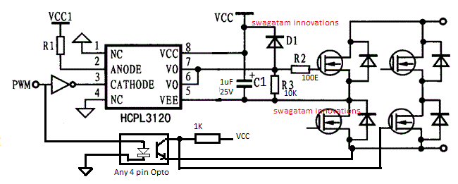
D1 can be 1N4148. other across the mosfets can be 1n5408. usually these are already present inside the mosfets…
Thanks sir. I very appreciate it. for the resistor, how about the power rating should I use? 1/4 W or bigger than that?
you can use 1/4 watt resistors since no high current is involved here.
Thank you for your suggestion. I will wait if you are willing to design with full bridge IC standard as you said. for the selection of high voltage opto by me is because I have referred to another website stating that HCPL3120 is Robustness, Real-estate, and Simplicity instead of using IR2110. If you have other ideas, which are relevant to the requirements of my project, I would appreciate it if you can help me create a circuit that works well based on the needs of this project.
Thanks!!!!
OK I’ll try to do it soon, and let you know….
yes. I would like to know how to implement the opto to control the MOSFET apart from using the component of discrete electronics. I intend to use four (IXFH22N60P3 – Power MOSFET, N Channel, 22 A, 600 V, 0.39 ohm, 10 V, 5 V) to create a full bridge network.
Maybe you can help me in terms of connecting and using other passive components to build this full bridge network such as the choice of appropriate value of capacitor, resistor, and diode by using HCPL3120 to drive the MOSFET
I have tried to do it here, you can check it:
here VCC1 = 5V
VCC = 12V
one side is shown, you will have to repeat the same layout for the other side of the bridge
I won’t recommend using discrete components as that wouldn’t guarantee accurate results, I’ll try to design it with a standard full bridge IC.
However I cannot understand why the high voltage opto is selected by you, any other low voltage opto can be also used because we are not connecting the opto anywhere along the BUS line of the mosfet, as far as I understand.
here the idea is to only ensure total isolation of the Arduino from the Full bridge network in every possible manner..
I’m done with the bipolar PWM for the full bridge with V/F control method using MATLAB/Simulink. the PWM signal (4 PWM signal) I was deployed to the hardware (Arduino). So I want to send the PWM signal to the HCPL3120 and drive the MOSFET. I realize that the HCPL3120 can reduce my component than I’m using IR2110 to drive the MOSFET.
Here the output PWM of the simulation for 0.02sec ( ).
). ).
). )
)
Here the PWM with LC filter for 0.02sec (
here the output waveform if I variable the modulation and the frequency (
any suggestion for me Mr. Swagatam?
OK so you want to know how the opto coupler can be integrated with a full bridge network in order to implement the full-bridge operation correctly? right?
and what is the specifications of the full bridge, should it be using 4 N channel mofets, because using 4 channel moefets will require a special driver IC. Although I have designed circuits without using driver ICs, I haven’t tested them practically.
Please clarify the above
I’m done with the bipolar PWM for the full bridge with V/F control method using MATLAB/Simulink. the PWM signal I was deployed to the hardware (Arduino). So I want to send the PWM signal to the HCPL3120 and drive the MOSFET. I realize that the HCPL3120 can reduce my component if I’m using IR2110 to drive the MOSFET. any suggestion for me Mr. Swagatam?
Great job
Hi,
Will it be possible to use a portable battery bank for phones to charge a laptop? I’m trying to use the USB output (5V/2.1A) as my source to the circuit. However, since SG3525 requires 8V and above, I’m thinking of boosting this 5V to 12V instead. I do not need it to supply enough capacity to charge a laptop fully but I just need it to work and be able to charge.
So far, I have made a SG3525 DC-DC Converter (push-pull) running at 180V. Didn’t focus much on the inverter part yet because I believe that most recent laptop chargers are SMPS-based and rectification should be the first stage so DC might be possible. I tested the output with a dummy load of 680ohms at 180V and managed to get 0.1A so I assume the DC/DC converter is working fine. Load is assumed to be about 70W for laptop. Issue is with the input side.
The issue is that my input source is not able to supply sufficient current. If my input voltage is 12V so for a load of 70W, my input current will need at least 5.83A which is too big for my application. I’m only able to supply 2.1A at most using the USB output of my port battery bank. Are there any ways to amplify the current using transistors or other methods at the source side? I have heard of methods to keep the average current constant but able to have certain pulses of current to be much higher (e.g. 5A) and with certain pulses to be lower but still average it out to be the current the source supply (e.g. 2.1A in my case).
Thanks.
Hi, Amplifying current would result in dropping the voltage, and vice versa, in other words the output wattage can never exceed the input wattage. In your case the input wattage us 12 x 2 = 24W, if you divide 24 with 180 it comes to around 0.13 amps, and this figure cannot be increased without decreasing the 180V level. Whether it is in the pulsed form or continuous the o/p IxV will be always less than the i/p VxI. For getting 70 watt output you will need an input higher than 70 watts
how many watts and is it sine wave?
no it is not a sinewave.
Hi swagatam
I made this circuit with the addition of extra PWM signals to the low side MOSFET, when testing the circuit without connecting the transformer it was working well (ie the voltage were out from it output that would have go in to the transformer terminal), but when I letter connect the transformer to the circuit, it blow up the MOSFET
Please what could be the reason for the cost of the damage of the MOSFET?
Because I wanted to make used of the circuit to replace a damaged H bridge inverter board
Hi Emmanuel,
Can you tell me, how did you test the circuit without the transformer? You can test test it using a resistive load such as a 12V or 24V car bulb and check if everything works correctly or not. This will confirm that your H bridge is working fine.
You can also connect 10 ohm resistors in series with the low side gates, and a reverse diode parallel with this resistor.
Also make sure your SG3525 output has sufficient deed time.
After this you can connect a small transformer and again confirm the results.
I will connect the 10ohms resistor together with the diode and I will also add protective diode from drain to source after then I will let you know the outcome
Thanks for your quick response
You must test with a real load such as a bulb or a motor etc….only that will confirm if your h bridge is working.
I have made the changes and even change the oscillator circuit from SG3524 to SG3525 circuit but when using it with small transformer it function very well and when attaching a 3.5kva transformer the BC547 at high side MOSFET will blowout immediately after turning ON, please what could be the problem or is it that the H bridge setup can’t power higher wattage system?
Hello Wagatam
Firstly I have to thanks you for your electronic aid, i made the above circuit several times but it doesn’t work with 150ah – 200ah of battery on no load but work fine in 50ah with any Load, but i discovered that inverted signal is the problem ( the signal doesn’t goto 0v) which cause the burning of the upper MOSFET, please what can which can be use to invert properly to give a full inverted signal
Thank you Abdulganiyu, You can connect a 4k7 resistor between the base/emitter of the two BC 547 transistors, and check the response. If 4k7 doesn’t work you can try 2k2 resistors. You can also connect a 1K between the gate/source of the lower mosfets for better response.
K thanks i will make the change and give you feedback soon
You can try adding a reverse diode across the emitter/collector of the BC547 and also a reverse diode across the base 10K resistor, and see if that helps!
the diodes can be 1N4148
I tested the circuit with the use of multi meter by setting it to voltage reading and read the voltage that is coming out from it output which would’ve been connected to the transformer input and the voltage reading was okey or couldn’t have tested it that way? l use SG3524 not SG3525 and I tested the oscillation circuit (ie SG3524 circuit) it was okey, I did that by connecting LEDs to it output pin and to the GND and it was oscillating well
Great work Swagatam the design is working well. Keep it on such a nice ideal. Aondofa Injoh from Nigeria.
Thank you Aondofa, i am glad it worked for you! keep up the good work!
Hello swag.my questions are simple, first. Can this h-bridge circuit be driven directly with a 24v battery system, secondly. Can the transformer be used to charge the batteries on utility mode. Then thirdly why are the MOSFETs not having gate resistor like other circuit s do. Thanks that all for now.
Hello Karlas, yes you can use 24V for the above shown H-bridge configuration.
The transformer can be used only in the inverter mode, it cannot be used for charging the battery unless some special changeover circuitry is incorporated.
the upper mosfets do not need gate resistor since the BJT's 1K itself forms the gate resistor for the mosfets…the lower mosfet could be added with a some low value gate resistor….although it's never too important.
Hello swag, can this circuit be driven directly with a 24vdc supply?secondly , can the same transformer be used to charge the batterywithout any damage to the MOSFETs? Then thirdly why are the MOSFETs not having gate resistor like 10 ohms or any other thank .Karlas is my name and a follower of this blog .
Hi Swagatam
Thanks for getting back to me in the pure sinewave inverter post.
I would like to know in this full bridge circuit above,if i have a 290v dc supply voltage from a high frequency source if the 10uf 50v capacitor must be changed to a higher voltage and if the irf540 must be changed as well to handle the higher voltage.I want to switch this high voltage DC to 220vac at 50Hz
regards Robin
Thanks for the update Robin,
sorry I could not get this: (source,1k,led,ground)
LED can be connect in series wit the BC547 base and across gate/source of the low side mosfet any other position could create problems wit the functioning or misleading indications.
Please let us know, if possible through images if the deign works for you correctly as proposed i the article…
wish you all the best..
Hi sir I appreciate the great gesture you are doing may the lord be your strength ????. Sir my question is : Can one parallel each of the mosfets to give a total of 8 instead of 4? And also will it be advisable to to supply the drains of the high side with a 24v but the gets with 12v? This is to say using like 7812ic to get the 12v from the 24v source. Thank hope to here from you soon.
Thanks Gody, yes you can parallel as many MOSFeTs as you want to reach the desired wattage level.
The drains can be supplied with any DC voltage depending upon the MOSFETs VDS rating, but the gates must not exceed 15 V. So your assumption is correct.
Hi Swagatum
I've been wrestling with this H-bridge circuit above and it worked the first time i made it,I slowed down the hz so i could see it oscillating,the moment i put a load on (bang).
Ok,I've now disected it and first got the two high side Irf840's blinking,(source,1k,led,ground),pin 11 to the one IRF gate and pin 14 to the other but as soon as i switch the sg3525 on both led's come on at the same time thereafter it oscillates normally,would'nt this be a catastrophic occurance?.By the way the cap seems to have charged up via the load because i was getting 18v on the gates.
Then i got the low side IRF's blinking(+12v,1k,led,drain,source,ground)pin 11 to 1k resistor then to gate,pin 14 same to other IRF but they would not oscillate without the 1k to the gate?
Oh! I saw your comments with Bob the Blogger(interesting)
Regards Robin
sure…thanks!!
Ok ,Thanks,I understand,will give it another go and let you know how it goes
Robin
Hi Robin, yes adding a slight delay or dead time will help to control mosfet burning..
you can add a resistor between gate and source if the mosfets are relatively away from the IC or the trigger source…
no it won't affect the above explained circuit…and please note that the BC547 emitters are only connected to the ground and not to the mosfet sources
Hi Swagatum
Ok on first attempt i burnt one of the IRF840's,so I'm just making sure that the resistor between pin 5 and 7 on the SG2535 causes a delay which it does.Also is'nt it a good idea to put a 1k resistor between the gate and source of each mosfet to make sure that it is not accidently on when you switch on,or would it affect the functioning of your circuit
Hi robin, as far as I think, the mosfet drains will need to be connected with the 290V DC, while the diode anode separately connected to the 12V supply…yes the mosfet will need to replaced with a 400V type for example IRF804 etc…
sir please is this full bridge circuit work and tested.100% working??
Abduleng, I have presented the concept after doing some intense research on the net, now it's upto the readers to decide whether it will work or not
Where is the sechmatic
you can use any standard IC SG3525 circuit and just replace its mosfet stage with the above shown full bridge mosfet stage…for example you can try the the circuit which is show here and combine its output with the above explained full bridge circuit:
Hello Sir,
I am working on Full Bridge Inverter Circuit using IGBTs where the DC Voltage is not constant at the input, I wanted to know about the protection circuits which must be designed to avoid any damage.
Prathamesh, since the inverter is being operated using a battery there cannot be any fluctuations, but an overload (overcurrent) could cause problems, for which you can use the shut down pinout of your full bridge IC to protect the system.
Thank you Sir, the link was very helpful. Also needed some help with Overvoltage and Overcurrent Protection Circuits. Will you please tell me the devices which must be used to protect the inverter from sudden fluctuations where the output of the inverter is 1.4kW with a nominal input voltage of 200V and maximum input voltage 250V?
I'd appreciate any information you could give me.
Hello Prathamesh, which cirucit are using using? is it using the IRS based full bridge driver? please provide the schematic details….if it's an IRS based driver, then yo can use its SD (shut down pinout for the protection feature…for other info you can study the following article:
https://www.homemade-circuits.com/2013/09/mosfet-protection-basics-explained-is.html
Sir I think your high side and low side GATEs are incorrect position or connection. Am I right?
that's wonderful, thanks for posting this valuable info!!
I checked again the drain/source as instructed, the drain/source voltage is 6.75V. I double checked the schematics and it's properly oriented. And it's all components are soldered in PCB.
Silverman, please help me with the diagram you buit including any changes you made so that I can implement it really to my project,I will really appreciate.
Thanks for the reply sir. My bad.. I forgot my basic voltage check. I put my test probe across to the connector of 12v windings of transformer and I got AC readings at 13.5vac.
It is now partially completed inside the wooden box. And I also made a changeover circuit and I Incorporate it to your design.
That's great silverman…I appreciate it a lot.
where exactly did you find 13.5V?
check it across drain/source terminals of the mosfet, you wlll find it to be around 6V,,,,that's the average value due to the ON/OFF cycles of a 12V supply
Hello sir.. good news! I finally build your design, and it's fully working. The output from the MOSFETs is 13.5vac using 12vdc/100ah battery. The output from the transformer is 240vac. My question is why 13.5vac output but my supply is 12vdc.?
I'm using IRF3205, my transformer build is 220v-12v with 60hz.
You are most welcome Silverman, all the best to you!
Thank you sir. I got now the idea of the bootstrapped implemented in your diagram. I already made your previous 1kw full bridge inverter and its fully functional. I'm now using it in my house to drive my appliances.
I will test this new inverter diagram and I will let you know sir.
Thank you very much sir for being helpful to us as a hobbyist.
Nope, I have already explained the reason in the above comment….
Hello sir in this post the pulse from the ic is not configured in a diagonal form as your other full bridge configurations , is this oversite or the correct configuration for this sequence?
Hello Ugoeze, it's because of the presence of the BC547 transistors which invert the signal for the upper mosfet making sure that the only the diagonal mosfets are triggered at any instant during the osculations.
Hello swagatan, please can ic sg3524 be used for this design? I can’t find sg3525 here in my location.
thanks
Hi Louis, yes it can be used
Pls sir, can i get a more modified H bridge circuits. with Ac input for charging
will try to get, if possible….