The transistorized low dropout voltage regulator circuit ideas explained in the following article can be used for getting stabilized output voltages right from 3 V and above, such as 5 V, 8 V, 9 V, 12 V, etc with an extremely low dropout of 0.1 V.
For example, if you make the proposed 5 V LDO circuit, it will continue to produce an output of a constant 5 V even if the input supply is as low as 5.1 V.
Audio/Video Representation
Better than the 78XX Regulators
For the standard 7805 regulator we find that they compulsorily need a minimum of 7 V to produce a precise 5 V output, and so on. Meaning the dropout level is 2 V which looks very high and undesirable for many applications.
The simple LDO circuits I have explained below can be considered better than the popular 78XX regulators like 7805, 7812 etc since they do not require the input supply to be 2 V higher than the intended output level, rather can work with outputs within 2% of the input.
In fact, for all linear regulators such as the 78XX or LM317, 338 etc the input supply must be 2 to 3 V higher than the interned stabilized output.
Designing 5 V Low Dropout Regulator
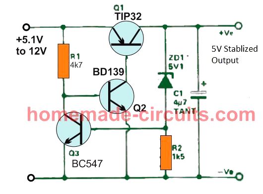
The figure above shows a simple low-dropout 5 V stabilized voltage regulator design that will give you a proper 5 V stabilized even when the input supply has dropped to less than 5.2 V.
The working of the regulator is actually very simple, Q1 and Q2 form a simple high gain common-emitter power switch, which allows the voltage to pass from the input to the output with a low dropout.
Q3 in association with the zener diode and R2 work like a basic feedback network which regulates the output to the value equivalent to the zener diode value (approximately).
This also implies that by changing the zener voltage value, the output voltage could be changed accordingly, as desired. This is an added advantage of the design since it enables the user to customize even the non-standard output values which are not available from the fixed 78XX ICs
Designing a 12 V Low Dropout Regulator
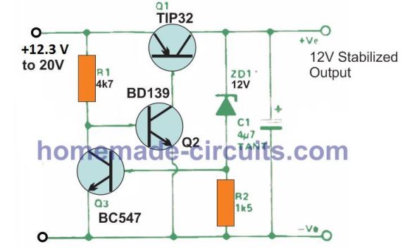
As explained in the previous section, merely changing the zener values change the output to the required stabilized level. In the above 12 v LDO circuit, we have replaced the zener diode with a 12 V zener diode to get a 12 V regulated output through inputs of 12.3 V to 20 V.
Current Specifications.
The current output from these LDO designs will depend on the value of R1, and the current handling capacity of Q1, Q2.
The indicated value of R1 will allow a maximum of 200 mA, which can be increased to higher amps by appropriately lowering the value of R1.
To ensure optimal performance, make sure that Q1, and Q2 are specified with high hFE, at least 50. Also, along with Q1 transistor, Q2 also must be a power transistor, as it might also get a bit hot in the process.
Short Circuit Protection
One apparent drawback of the explained low drop circuits is the lack of short circuit protection, which is normally a standard built-in feature in most normal fixed regulators.
Nevertheless, the feature can be added by including a current limiting stage using Q4 and Rx as shown below:
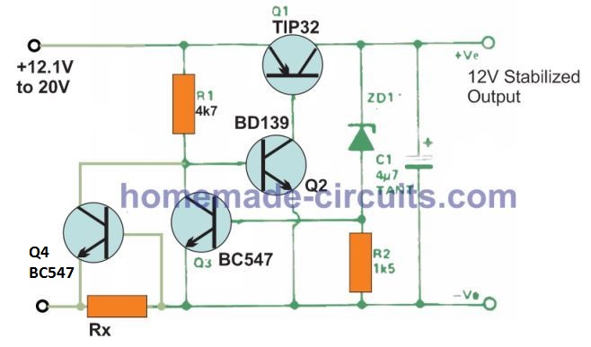
When the current increases beyond the predetermined limit, the voltage drop across Rx becomes sufficiently high to turn ON Q4, which begins grounding the Q2 base.
This causes Q1, Q2 conduction to become highly restricted, and the output voltage shuts down, until of course the current draw is restored to the normal level.
Low-Drop Transistor Regulator with Soft Start
This high gain voltage regulator using just a couple of transistors includes qualities better than those of the widely used multiple emitter-follower variants.
The circuit had been tried in a 30 watt stereo amplifier that strictly demanded a highly regulated supply and also an output voltage which could climb slowly and gradually through zero volts to maximum, whenever the circuit was initially powered up.
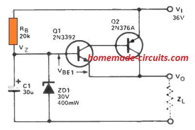
This soft-start plan (around 2 seconds) for the power amplifiers helped the 2000 uF output capacitors to charge without triggering too much collector current within the output transistors.
Normal regulator output impedance is 0.1 ohm. Output voltage is found by solving the equation by:
VO = VZ - VBE1.
The rise time of the output voltage is evaluated by calculating through the formula:
T = RB.C1(1 -Vz/V ).
A number of digital devices call for a preset switch on sequence for their power supplies. By establishing proper RB/C1 values, the rise time of the circuit's output could be fixed to deliver this sequence or delay interval.
Adjustable LDO Circuit
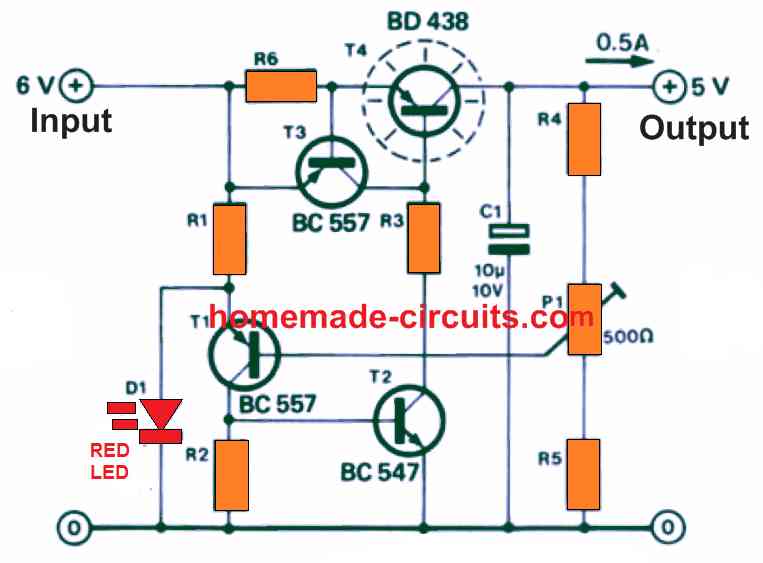
As can be in the schematic, the load is attached to the collector pin of the series transistor T4.
This indicates that this particular transistor could be turned ON hard into saturation, causing the voltage between emitter and collector to be just an extremely tiny saturation voltage.
This specific voltage level is dependent naturally on current specification and the type of the transistor.
Parts List
- R1 = 1k Ohms
- R2 = 10k
- R3 = 470 Ohms
- R4 = 1.2 k
- R5 = 560 Ohms
- R6 = 1.6 Ohms
- P1 = preset 500 Ohm
- C1 = 10uF/25V
- T1, T3 = BC557
- T2 = BC547
- T4 = BD438
- LED = RED 20mA 5mm
In the case of the discussed design considering a optimum current of 0.5 A the voltage drop will probably be hardly 0.2 V.
Combine with this the voltage drop around R6, necessary for current limiting. With roughly 0.5 V across R6, T3 begins conducting and restricts the output current.
LED D1 possesses a couple of functions, it works as an indicator and also as a voltage reference diode in order to clamp a 1.5 V to 1.6 V refernce level at the emitter of T1.
The base drive current for T1 comes from the voltage divider which involves R4, P1 and R5. With respect to the difference between the reference and output voltage levels, T1 slowly starts conducting.
Exactly the same then happens with T2 which provides more or less base drive to T4. The function of capacitor C1 is to filter the output stage.
You can easily replacing BD 438 with other popular brands, for example like BD136, BD138 and BD140 etc.
Having said that, these transistors may likely posses a rather increased saturation voltage. It should be observed that because D1 works like a reference source, it should be be a red-colored LED, other color LEDs may have other voltage drop specifications.
How to Design a Low Dropout Voltage Regulator using Transistors
Contributed by : Carl
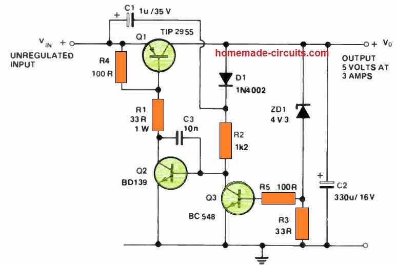
I needed a voltage regulator with an extremely low dropout voltage, capable of delivering a stable 5 V at approximately 3 A. Since numerous three-terminal regulators possess a dropout of 2.5 V or more, I designed the LDO circuit described below employing discrete components.
Although fairly straightforward, this low dropout voltage regulator design demonstrated performance on par with that of integrated circuit (IC) regulators.
The schematic of the prototype is displayed in the Figure below, yielding the subsequent test outcomes:
- Dropout voltage (@ 3 A): 0.75 V
- Load Regulation (0-3 A): Below 10 mV
- Line regulation (Vin 6 — 15 V): Below 10 mV
- Ripple rejection (@ 3 A): -63 dB
- Output (no load): 4.96 V
Alterations in the output voltage resulting from shifts in ambient temperature will primarily hinge on the traits of the zener diode, ZD1, and transistor Q3.
Consequently, it is imperative to maintain these elements away from heat sources, such as the heatsink for Q1 and the power transformer.
As the current configuration of the circuit currently lacks a precisely defined current limit, this capability can be incorporated by integrating the components portrayed in the Figure below.
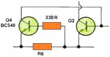
However, doing so will result in a 0.5 V increase in the dropout voltage. Alternatively, you can establish a current limit without heightening the dropout voltage by loading the output to the desired maximum current and incrementally augmenting the value of resistor R1 until the output voltage starts to decline.
The downside of this method is that RI must be chosen through experimentation and may necessitate recalibration if Q1 is ever replaced.
Consequently, if a current limit is imperative and a minor elevation in dropout voltage is tolerable, the procedure depicted in the second figure above is the preferred choice.
Another noteworthy trait of this circuit is its capacity to automatically deactivate should a substantial load cause the output voltage to plunge beneath roughly 1.2 V.
To restart it, you must disengage the input voltage (or power down the mains), wait several seconds, and then reapply power. Simply unburdening the load will not enable a restart.
Components C1 and D1 serve as inception components, ensuring dependable starts even with markedly capacitive loads.
To adapt the circuit for varying voltage and current requisites (up to approximately 5 A), adhere to this streamlined design methodology:
- Determine the output voltage, Vo (5 V).
- Elect the maximum current, Io (3 A).
- Choose a fitting transistor for Q1 (TIP2955, 70 V, 10 A).
- Calculate R1 max: Vo / (Io / (Q1 hFE)) = 5 / (3 / 20) = 33.3 ohms or simply 33 ohms.
- Compute the dissipation of R1: Vo^2 / R1 = 25 / 33 = 0.75 W (employ a 1 W resistor).
- Select an appropriate device for Q2 (BD139, 80 V, 1 A).
- Determine R2 max: Vo / (Io / (Q1 hFE) * (Q2 hFE)) = 5 / (3 / 20 * 40) = 1300 ohms; employ a 1k2 resistor.
- Assess the dissipation of R2: Vo^2 / R2 = 25 / 1200 = 21 mW.
- Choose an apt device for Q3 (BC548, 25 V, 100 mA).
- Pick a zener diode, ZD1, possessing a voltage of Vo - Vbe (Q3) = 5 - 0.65 = 4.35 V (utilize a 4V3 zener). As the current coursing through Q3's base typically remains minute, a low-wattage 400 mW or 1 W zener can be utilized.
- Compute R3 to bias the zener: I2 = 0.2 * (P2 / V2) = 0.2 * (0.4 / 4.3) (assuming a 400 mW zener) = 18.6 mA. Ergo, R3 = 0.65 V / 18.6 mA = 35 ohms (use a 33-ohm, 1/4 W resistor).
- R4 serves to forestall Q1 from activating due to leakage; its precise value is not crucial, and a 100-ohm, 1/4 W resistor is generally fitting.
- R5 serves as a precautionary measure to confine excessive current through Q3's base and can be 100 ohms.
- C1 serves as the startup capacitor, and any capacity between 1 uF and 4.7 uF should suffice, with a voltage rating surpassing Vin.
- C2 is employed for stability, with an appropriate value being 100 uF per amp of load current. A 330 uF capacitor was employed in the prototype, and its voltage rating should exceed the output voltage rating.
- C3 is indispensable for stability and should be around 10 nF.
- Mount Q1 on an appropriate heatsink, contingent on the power it dissipates, which should be modest if Vin-Vout is low.



Questions & Answers
Hi I made the simulation of Low Dropout Linear Voltage regulator, the last circuit. I am not able to drive 3A in the load. The input is a 12V sine wave at 50Hz which goes through a bridge rectifier and then that is given to the TIP 2955, can you help with it?
Hi, can you please disable or remove the Q3 stage completely and check again?
I did that two ways. I removed Q3 and 100R and grounded instead but that was of no use but then I connected BD139 base to zener without ground and imptroved result to give 5V 3A but input had to be 50V sadly. Any leads to get same result with 10V min will help with justification?
In that case I think you should try the first circuit, which is a basic design and should work perfectly.
You can replace TIP32 with TIP2955, just make sure to add a series base resistor.
Hello again. Ty for your help. The problem was in rectifier and when I changed the cap to 1mF it worked fiine. Now am using TIP 32C instead of TIP 2955, but the max am being able to drive yet is 1.8A, how can I get to 3A max?
Glad you could solve the issue correctly.
To increase current, you will need to change the transistor.
You can probably try a Darlington version, using TIP147 and check the response…
I have tried multiple times to debug it. My implementation works on breadboard but does not on pcb and the paths aren’t even short. what do I do? the transistors are fine too.
If it is working on breadboard then it should certainly work on a PCB too, please check each and every connections carefully, and check the pin orientation of the components also, you will be able to trace out the fault.
There’s a small mistake in the “Adjustable LDO Circuit”.
In order to have sufficient voltage drop between the unregulated input and D1 (LED), R1 needs to be at least 270 ohm and more suitable 1K.
In order to reduce power in the reference circuit ( T1 ), I would use a 3,3V zener instead and design the feedback circuit to a voltage around 2,7V. ( 2mA in each of these should be enough. )
In order to have better symmetry in the driver section, R3 can be changed to 1K.
It was probably taken from the elector electronics magazine, anyway thanks for the analysis, yes the LED resistor should be around 1k…
Hello Swagatam,
I’d like to introduce your website in my personal blog.
All the reference will be shown with your web link and name.
Is that OK?
Thanks
Wei
No Problem Wei, you can do it.
Hello! newbie here, in the “5 V Low Dropout Regulator” is there a reason why you are using those specific transistors? (sorry, english is not my main language), Regards!
Hi, the transistor values are not critical and can be replaced with any other values depending on the current (ampere) specifications of the load.
Really like your design. What would be necessary to modify so that I can use an Input Voltage from 12 to 24V with 12V as Output? Thank you
Thank you for your feedback, I appreciate it.
Yes you can use 24V also in the above circuits without any changes.
To get 12V output, you just have to set the zener diode to 12V or to a nearby value so that the output is fixed to 12V.
Thanks for the info. Another quick question. How can I implement a reverse-polarity safety using a transistor or a N-MOSFET in the circuits above? Thanks.
I think that can be simply done by adding 1N4007 diodes in series with the emitters of Q2 and Q3
Is there free or low online course.
If any one have, kindly share the link to me.
Am interested to study electronic development. Thank you
There are no specific links for the course. It is an extensive ongoing process where you will have to first learn the basic working of the electronic components and then learn how to build small circuit projects using these components. You will have to combine this with practical constructions.
Hello
I want to use the stabilized 12V LDO with 6A but with Mosfet so I replace Q1 by a irf 9540n or irf 9540p and rest of the circuit remain same. only for the Rx value. i am taking 0.1 ohm 5w resistor .will this work properly ? and do i have to use that 1k ohm resistor between mosfet gate and bd139 collector.?
Referring to your 12v LDO short circuit protection circuit
Thanks
To build a high current version of the 12V LDO using p-channel mosfet, you can apply the following design:
hi swagatam
i’m gonna build with this mosfet version
is it correct for the IRF9540 pin in the schematic?
as i saw that pin SOURCE of mosfet take the voltage input and the output voltage is pin DRAIN
Hi Andre,
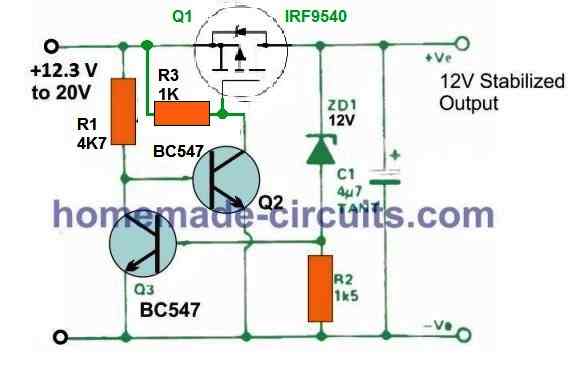
sure, you can try the following MOSFET LDO design:
The pin connections are correct, the SOURCE is connected to the input supply and DRAIN to the output load.
oh I see. Thank you so much for the detailed image helps a lot and attachment of additional short protection circuit will be same as previous one?
You are welcome, yes the short circuit will be the same as indicated in the 3rd diagram.
Hi,
I’m stuck please help Me!!! I want 12V uniform with 6A draw, as my load is 2.5A max but are two in number and connected in parallels means total 5A draw and as an power supply I have 12v 7ah battery .so IN short using your 12V Low-Dropout Regulator with short Circuit protection is right choice but I don’t know how to use your circuit to get desired output. so please guide me what changes have to do I am total new to this.
Hi, you can try the last circuit which is also short circuit protected.
For 6 amp handling capacity, you will have to replace T4 with TIP36 transistor, and T2 with 2N2222 or 8050, and also replace R3 with a 100 ohm resistor.
R6 will be = 0.6 / 6 = 0.1 ohm
wattage will be = 0.6 x 6 = 3.6 watts or 5 watt.
Thank you for your answer. i will try it and let you know
Sure, no problem!
Hello, sir
I want to use your 12v low dropout circuit and i want an 12v 10Amp constant supply ..what should i do ? i mean do i have to change something from this circuit or have to make an current boost circuit and connect it in parrallel with this..
Hello Ethan, you can replace the TIP32 with an IRF9540 mosfet, and check how it responds at 10 amps. No other changes would be required.
Thank you sir
Hi, thanks for this schematics.
I’m wondering, can I use this circuit to charge a battery safely or if the power supply turn off the reverse current provide by the battery will burn out the circuit?
Hi, you can use this circuit to charge your battery safely, the reverse voltage from the battery will not affect the transistor since due to the absence of the base bias the BJT will be turned OFF which will not allow the reverse voltage to get though the transistor.
Hi mr swag..
Thanks for reply and suggesting this circuit, so by replacing few componenets specialy R2 1K5 with pot 10K i can get variable output starting from 0.1volt..awesome..
Thanks & keep inspiring.
You are welcome Mp, yes as per the working specifications of the circuit, it should be able to do the job for you!
Hello and thank you for the diagram
If I want to use the 12V LDO with 10A, I replace Q1 by a TIP36 and do I also have to change the value of R1 ? And for the Rx value, it is 0.6/10 = 0.06Ohm and 0.6×10= 6W, right?
Could a 5W resistor do it?
Thanks
Yes the R1 value will depend on the value of the resistor which must be included at the Q1 base.
Q1 base resistor can be calculated using the following formula:
R = (Supply – 0.7) x hFe / 10
Once this is found, using Ohms law we have to determine the current that may flow through this resistor, and then calculate R1 using again the same formula as above, but with the figure 10 replaced with the figure obtained from the Ohm’s law.
The Rx value and wattage calculations are correct
Thank you very much
I want to build the 12 V Low-Dropout Regulator for the CPE of the fibre network. The transformer rated 12V 1A. So I want a current of 1.2 to 1.5A but cannot test the amps or calculate the value of the resistor.
The power is from my solar system and the volts vary between 12.3 and 14.
Regards
Klaas Nel
You can try any of the circuits explained above for your application, all will provide you with the intended LDO results
Hello sir, Can this circuit be powered & used with solar panel to charge mobile safely.
Solar panel spec. is
3.5 watts peak power Output.
Power Current: 390 ma (Max)
Power Voltage : 9V (max)
Open Circuit Voltage : 10.2 V
Thanks in advance.
Hello Pratap, yes you can use the circuit for your solar application safely, but make sure to confirm the results with a multimeter and a dummy load before connecting a mobile.
Good Morning
Grateful for the response and attention
Thank you, appreciate your feedback!
good afternoon
I’m looking for a circuit like that with discrete components, don’t you have a similar circuit with a mosfet?
grateful for the attention
Hi, You can try replacing Q1 with a MOSFET and check the results.