Here we are going to discuss about LM393 that is a very popular dual voltage comparator IC. I will try to explain everything step by step so you can understand. We will see the ratings, the pinout, the electrical values, the formulas and also the way we can use it in real life circuits.
General Overview
We can say that LM393 is basically a dual open-collector comparator. That means inside there are two comparators. Each comparator has a non-inverting input marked with + and an inverting input marked with −. It also has one open-collector output.
Now that output will only sink current and it cannot source. So you must always use one external pull-up resistor for making the output work properly.
Since this IC works on single supply and also on split supply, so you can use it for many applications. We see that the input range includes ground, which makes it very useful for battery operated circuits.
If you want a quick audio/video explanation, you can prefer watching the following video:
Pinout Explanation

Now let us see the pinout step by step. We consider the DIP-8 package as the reference.
- Pin 1 is OUT A, this is the output of comparator A.
- Pin 2 is IN− A, this is the inverting input of comparator A.
- Pin 3 is IN+ A, this is the non-inverting input of comparator A.
- Pin 4 is GND, this is the ground supply pin.
- Pin 5 is IN+ B, this is the non-inverting input of comparator B.
- Pin 6 is IN− B, this is the inverting input of comparator B.
- Pin 7 is OUT B, this is the output of comparator B.
- Pin 8 is VCC, this is the positive supply pin.
| Pin (DIP8/SO8) | Name | Function |
|---|---|---|
| 1 | OUT A | Open-collector output of comparator A |
| 2 | IN− A | Inverting input comparator A |
| 3 | IN+ A | Non-inverting input comparator A |
| 4 | GND | Ground (negative supply) |
| 5 | IN+ B | Non-inverting input comparator B |
| 6 | IN− B | Inverting input comparator B |
| 7 | OUT B | Open-collector output of comparator B |
| 8 | VCC | Positive supply |
Absolute Maximum Ratings
Now let us talk about the limits that you must never exceed. Because if you cross these values then the IC can get damaged.
- Supply Voltage VCC is allowed from −0.3 V up to +36 V.
- Differential Input Voltage Vid is allowed up to ±VCC.
- Input Voltage Vin can be from GND −0.3 V up to VCC +0.3 V.
- Output Current IO can go up to 50 mA in short pulses but recommended continuous sink is less than 20 mA.
- Power Dissipation PD depends on the package and ambient temperature.
- Junction Temperature TJ maximum is +150 °C.
- Storage Temperature Tstg is −65 °C to +150 °C.
- ESD Rating is typically 1 to 2 kV.
| Parameter | Symbol | Limit |
|---|---|---|
| Supply voltage (VCC) | VCC | −0.3 V to +36 V (tested to 30 V typical). Do not exceed 36 V. |
| Differential input voltage | Vid | ±VCC (i.e. up to ±36 V) |
| Input voltage (any input) | Vin | GND −0.3 V to VCC +0.3 V (for VCC ≤ 36 V) — do not exceed supply rails except as allowed by manufacturer note |
| Output current (continuous, per output) | IO | Short pulses up to ~50 mA possible; recommended sink ≤ 20 mA — excessive IO can overheat and damage device |
| Power dissipation | PD | Limited by package thermal resistance and TJ(max) (check vendor-specific Pd at given ambient) |
| Junction temperature | TJ | +150 °C (check vendor spec) |
| Storage temperature | Tstg | −65 °C to +150 °C |
| ESD rating (HBM) | — | Typically 1–2 kV (varies by vendor/grade) |
Recommended Operating Conditions
- Supply Voltage VCC is recommended from 2.0 V to 36 V.
- Input Common-Mode Range VCM is from GND to (VCC − 1.5 V).
- Ambient Temperature TA is from 0 °C to +70 °C for normal grade and −40 °C to +85 °C for industrial grade.
| Parameter | Symbol | Range / Typical |
|---|---|---|
| Supply voltage (operating) | VCC | 2.0 V to 36 V (commonly used 5 V, 12 V, 15 V). |
| Input common-mode range | VCM | From GND to (VCC − 1.5 V) typical (i.e., includes ground). |
| Ambient temp (commercial grade) | TA | 0 °C to +70 °C (some versions −40 to +85 °C). Check vendor grade. |
Electrical Characteristics
Now let us study the most important electrical numbers of LM393.
- Supply Current ICC is around 0.4 mA typical for each comparator.
- Input Offset Voltage VIO is around 1 mV to 5 mV typical, but maximum values are higher.
- Input Bias Current IIB is around 25 nA typical.
- Input Offset Current IIO is few nA typical.
- Input Common-Mode Range VCM is from 0 V to VCC − 1.5 V.
- Output type is open-collector NPN.
- Low Level Output Voltage VOL is around 0.08 V to 0.3 V typical depending on sink current.
- Maximum recommended Sink Current is around 20 mA.
- Propagation Delay tPD is typically 1.3 µs, depending on input overdrive and load.
- Response Time can be 200 ns up to few µs based on the test.
| Parameter | Symbol | Typical | Notes / Conditions |
|---|---|---|---|
| Supply current per comparator | ICC | 0.4 mA (typ) | Low and largely independent of VCC. |
| Input offset voltage | VIO | 1–5 mV (typ) | Offset maximum over temp may be several mV (datasheet lists max e.g., ±2–5 mV typical family). |
| Input bias current | IIB | ~25 nA (typ) | Very small, but matters for very high-R dividers. |
| Input offset current | IIO | few nA (typ) | — |
| Input common-mode range | VCM | 0 V to (VCC − 1.5 V) | Includes ground; upper limit about VCC − 1.5 V. |
| Output type | — | Open-collector NPN | Requires pull-up resistor to VCC or other rail; output cannot source current. |
| Low-level output voltage (saturated sink) | VOL(sat) | ~0.08–0.3 V typ (depends on sink current) | For small sink currents (e.g., 0.4 mA) low; rises with larger sink. |
| Maximum sink current (recommended) | IO | ≤ 20 mA recommended; continuous higher currents risk overheating | Datasheets warn about output short circuits. |
| Propagation delay (to change output) | tPD | ~1.3 µs (typ) | Depends on input overdrive and load; not as fast as logic comparators. |
| Response time (RL pull-up to VCC=5V, input overdrive) | — | 200 ns to a few µs depending on conditions | See datasheet graphs. |
Internal Behavior
Inside LM393 the input stage is made with a differential transistor pair. That is why it can sense voltage near ground. But it cannot go to full VCC at the input side.
The output transistor is open-collector type. That is why it only sinks.
So you need to connect a pull-up resistor externally. Since it is open-collector so you can also tie multiple outputs together to create wired-AND logic.
Practical Formulas And Examples
Pull-Up Resistor
Now let us find the formula for pull-up resistor.
When the output is low, the current through Rpu is VCC / Rpu. That current is sunk by the output. So we must keep it less than 20 mA.
Formula:
Rpu_min = VCC / IO_sink_allowed
Example: VCC = 5 V, maximum sink current = 10 mA
Rpu_min = 5 V / 0.01 A = 500 Ω
So we can select 2.2 kΩ to 10 kΩ normally.
Also the rise time of the output is calculated with:
t_rise ≈ 2.2 * Rpu * Cload
Comparator Hysteresis
We must add hysteresis then if the input is noisy. Because without hysteresis the output may chatter.
For non-inverting comparator,
Vth+ = Vcc * (R1 / (R1 + R2))
Vth− = VOL * (R1 / (R1 + R2))
Where R1 and R2 form the feedback divider.
Input Divider Error Due To Input Bias
We must also check the divider resistance then if input bias is important. Because input bias current creates offset.
Error = IIB * Rth
Where Rth is Thevenin resistance of divider.
Example: IIB = 25 nA, Rth = 100 kΩ
Error = 25e-9 * 100e3 = 2.5 mV
Propagation Delay And Overdrive
Propagation delay reduces then if you increase the input overdrive (Vin − Vth). Typical tPD is 1 µs to 2 µs.
Application Circuits
LM393 can be used for:
- Battery Low Indicator using divider and LED driver.
- Window Comparator using two comparators.
- Zero Cross Detector using divider and hysteresis.
- Open-Collector Logic Interfacing using multiple outputs tied together.
Thermal And Layout Notes
- We must not sink more than 20 mA continuously because then the package may overheat.
- We must always use a 0.01 µF to 0.1 µF capacitor near VCC pin.
- We must give small hysteresis to avoid noise oscillation.
- We must tie unused inputs to ground or to VCC through resistor and never leave them floating.
Family Members
LM393 belongs to a family which includes LM193, LM293, LM2903 and LM393B. These are compatible but have different grades like industrial or automotive.
Pitfalls
- The input cannot go fully to VCC because the common-mode stops at VCC − 1.5 V.
- The output cannot source current because it is open-collector.
- Large divider resistances will create error due to input bias.
- Shorting outputs to VCC or using large sink current continuously may damage IC.
Example Design Calculation
Suppose we want battery low detection at 11.0 V. VCC = 12 V, comparator reference = 2.5 V.
Equation:
2.5 = 11 * (R2 / (R1 + R2))
So R2 / (R1 + R2) = 0.22727
If we select R2 = 22 kΩ, then R1 = 75 kΩ.
Now Thevenin resistance Rth = 75k || 22k = 17 kΩ
Error due to bias current = 25 nA * 17k = 0.425 mV
At battery side this is equal to 1.87 mV error, which is negligible.
How LM393 Works As A Comparator
We first remember that LM393 is an open collector type comparator, that means the output pin does not generate a high by itself but it can only pull the output low towards ground. Please refer to this internal structure diagram, and see Q16 which forms the open collector output. So if you want to see a high at the output, then you must connect a pull up resistor from the output pin to Vcc.

Understanding The + and – Input Behavior
Let us say we have two pins, one is the non-inverting input which is marked as +, and the other is the inverting input which is marked as –. Now the whole game of the comparator is about comparing which of these two voltages is higher.
- Case One: Voltage at + input is higher than – input
When the + pin has a voltage greater than the – pin, then the internal transistor inside LM393 remains switched off. So then the output pin becomes open and through the external pull up resistor it rises close to the supply voltage Vcc. That is why we say the output is logic high in this case. - Case Two: Voltage at – input is higher than + input
When the – pin gets a voltage higher than the + pin, then the internal transistor becomes switched on strongly. So then the output pin is immediately pulled to ground, that is logic low. - Case Three: Voltage at + input is exactly equal to – input
In that condition the IC may go into uncertain zone, because of offset voltage and tiny noise. So then the output may jitter between high and low or settle depending on which side goes slightly higher. This is why in real circuits we usually add hysteresis with a resistor feedback, to avoid unwanted oscillations.
Output Stage Behavior
We must not forget that LM393 output is open collector. This means it can only sink current but not source current.
So then, you can connect the pull up resistor to any voltage level up to 36V (but inside allowed limits), even if the supply of the chip is lower and the output will follow that logic swing. This is very useful for interfacing with logic families of different voltage levels.
Step By Step Summary
So now let us put it very clearly:
- If V+ > V–, then output = HIGH (through pull up).
- If V– > V+, then output = LOW (pulled to ground).
- If V+ ≈ V–, then output is uncertain, may oscillate without hysteresis.
LM393 Relay Driver Comparator Circuit Example
What We See In This Diagram
So here we see that one LM393 comparator IC is drawn in the middle. On the left side we see two input pins, one is + input and the other is – input. On the right side we see that there is one output pin.
That output pin is not going directly to the load but it is first going to a 10k resistor and from there it is going to the base of BC547 transistor.
The collector of BC547 is connected to one side of relay coil and the other side of relay coil is at +12V supply. Also one diode 1N4007 is placed across the relay coil. The whole circuit is powered from +12V DC and 0V ground.
How The Input Section Works
So now let us see how the input section behaves. We feed two voltages, one voltage at the + input and another voltage at the – input. The comparator does not care about the absolute value but it only cares which one is higher. Now if the + input voltage becomes higher than the – input voltage then the internal transistor inside LM393 remains OFF and then the output pin becomes open.
Because of that, the 10k pull up resistor immediately pulls the output pin towards +12V and makes it HIGH.
But if the – input voltage becomes higher than the + input voltage then the internal transistor of LM393 becomes ON and then it pulls the output directly down to 0V ground and makes the output LOW.
Role Of The 10k Pull Up Resistor
Since LM393 has got open collector type output, it is unable to generate a HIGH level by itself. So for this reason we always connect one pull up resistor, here it is 10k.
Now if the LM393 transistor goes OFF then this resistor makes the output go HIGH. But if the LM393 transistor goes ON then this resistor is bypassed and the output is pulled to ground LOW. So this resistor is like a helper that decides the HIGH level.
Relay Driver Operation
Now let us see what happens to the relay driver side. The output of LM393 is tied to the base of BC547 through the same 10k resistor. So now when the LM393 output goes HIGH, that happens only when + input is higher than – input, then the base of BC547 receives current through 10k resistor and then BC547 switches ON.
So when BC547 switches ON, the collector current flows from +12V through the relay coil into BC547 to ground and the relay gets energized and its contacts close.
But if LM393 output goes LOW, that happens only when – input is higher than + input, then the base of BC547 gets no current, so it switches OFF. Then the relay coil does not get any current and it becomes de-energized and its contacts open.
Role Of The 1N4007 Diode
We must also notice the diode 1N4007 placed across the relay coil. This diode is for killing the high voltage spike which always comes when the relay coil is suddenly switched OFF. Without this diode the spike may burn the BC547 or even the LM393. So this diode is a safety part.
Summary Of The Working
So when + input is higher than – input then the output of LM393 becomes HIGH through the pull up resistor and then BC547 gets base current, so BC547 turns ON, relay switches ON.
But when – input is higher than + input then the output of LM393 becomes LOW to ground, so BC547 does not get any base current, it remains OFF, relay also remains OFF.
So we see that this circuit is nothing but a very simple comparator stage that is controlling a relay using a transistor driver and a pull up resistor.
Inside Circuit Structure Of LM393

So we first see that LM393 inside is made from many small transistors and resistors. It is not a magic box, but it is only some basic building blocks like differential pair, current mirror, level shifter and finally a big transistor for output.
When we look at Q4 and Q5, that is the main heart, the differential pair. The + input goes to Q4 and the – input goes to Q5. Now both of them share the same current, so whichever input is higher voltage, that transistor will pull more current.
So if + input is higher then Q4 dominates and if – input is higher then Q5 dominates. That is where the actual comparison happens.
Now we see Q1, Q2, Q3 and resistors R1, R4. These parts make a biasing network and current source and make sure that Q4 and Q5 always get a fixed steady current to fight with. Without that the circuit will not behave like a comparator.
Then we see Q8 and Q9, they form a current mirror which takes the imbalance from the differential pair and copies it to another side.
So even if the difference in voltage between + and – is very tiny, this mirror makes it into a larger current change. This way the signal gets amplified and clear.
After that the signal goes into transistors Q6, Q10, Q11 and also through some diodes you see there which work like intermediate gain stages and also level shifters. They keep the signal stable, they stop noise and they allow the circuit to work correctly even when the input voltages come very close to ground.
Then at the final part we see Q14, Q15 and the big one Q16 which are the output transistors. Q14 and Q15 drive Q16 and Q16 is the one directly connected to the output pin.
Q16 is an open collector type, which means it can only pull the output down to ground, it cannot push it up. So you always need a pull up resistor from the output to Vcc, otherwise the output will not rise high.
Now if + input is higher than – input, then Q4 wins, then the output transistor Q16 remains off so the output pin is pulled high through the pull up resistor.
But if – input is higher than + input then Q5 wins, Q16 switches on hard and the output pin is pulled down to ground. That is exactly how the comparator works inside.
So in the end the whole big circuit is only doing one thing, that is watching the voltage difference between + and – inputs and then using many small transistors to finally make the output transistor either off or on.
Conclusion
So we can conclude that LM393 is a simple but very powerful dual comparator. We can use it in many circuits. But we must respect its limits and use correct resistor networks. If we follow the proper design then it will work very reliably in all applications.


Comments
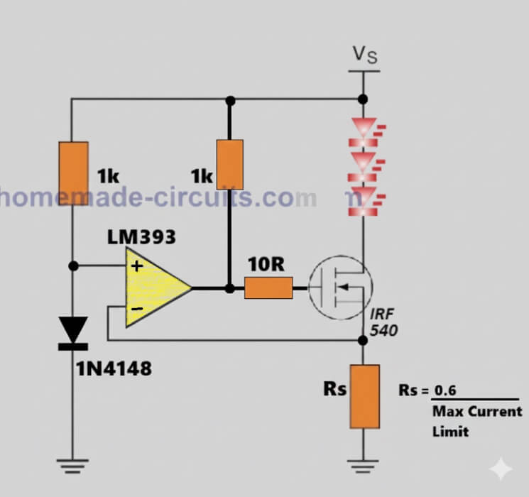
HOW TO USE OUTPUT OF LM393 WITH H BRIDGE TO DRIVE TWO MOSFETS AND CURRENT SENSING. INPUT, 12VDC, 490HZ, PWM. OUTPUT REQD 12V, 100W.
HOW TO USE LM393 FOR CONSTANT CURRENT 100W, 12V DC LED DRIVER. INPUT IS 0 TO 5V 490HZ PWM
You can do it in this way: