The IC 4047 is one of those devices which promises an unlimited range of circuit application solutions. The IC is so versatile that on many occasions it easily outsmarts it's close rival, the IC 555, let's study the datasheet and pinout details of this versatile chip.
Main Datasheet and Specifications:
In-built oscillator with variable frequency option through an external RC network.
Complementary push-pull outputs with a separate active clock output, the clock output is actually an extension of the internal oscillator frequency output.
Duty cycle locked to 50% for precision, fail proof operation of the external stages.
The IC 4047 can be configured as a free running astable MV, and also as a monostable MV.
In the astable mode the chip provides the option of integrating external triggering inputs, also called true gating and complement gating modes.
The monostable mode enables positive edge triggering as well as negative edge triggering of the IC.
It further allows retriggerable feature for extending the output timing to the desired calculated level. Meaning after the normal trigger is applied to the IC, more number subsequent triggers can be applied so that the output adds up the timing, generating further delay at the output.
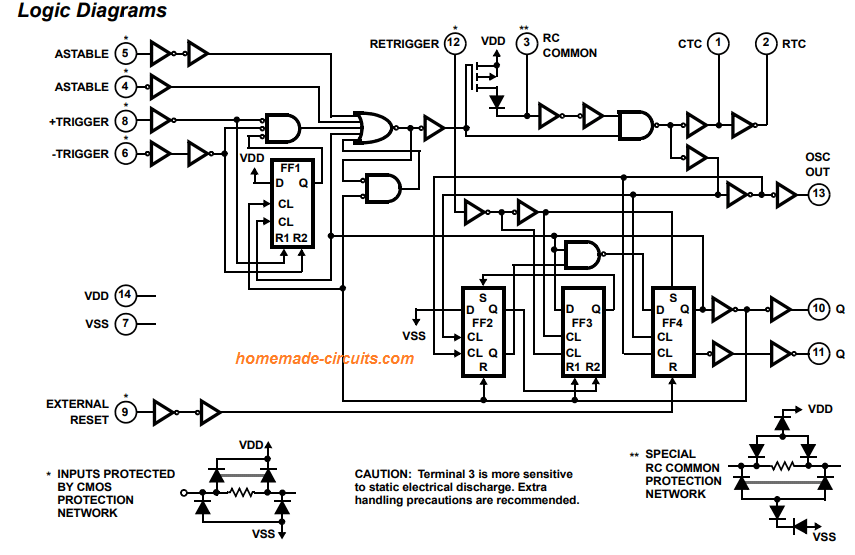
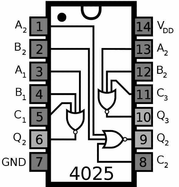
Internal Logic Diagram
Pinout Details
The following explanation suggests how the pinouts of the IC 4047 may be configured for implementing the above discussed operating modes:
In the free running astable mode, connect pins 4, 5, 6, 14 to positive or Vdd, connect pins 7, 8, 9, 12 to ground or Vss.
Vdd must be supplied with a recommended 3V to 15V and maximum 18V (absolute).
In gated astable mode connect pins 4, 6, 14 to positive or Vdd, connect pins 7, 8, 9, 12 to ground or Vss, connect pin 5 to the reset pin of the external trigger IC, while output of the external chip to pin 4 of the IC 4047.
For the above modes, the output may be obtained across pin 10, 11 (push-pull) while clocks at pin 13.
In positive trigger monostable mode, connect pins 4, 14 to positive or Vdd, connect pins 5, 6, 7, 9, 12 to ground or Vss, connect pin 8 to the reset pin of the external trigger IC, while output of the external chip to pin 6 of the IC 4047.
For the above modes, the output may be obtained across pin 10, 11.
Fundamental Free Running Astable Mode Circuit Diagram Using IC 4047
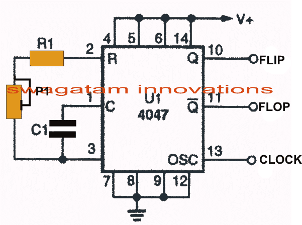
As shown in the figure above, the IC 4047 can be used as a free running astable multivibrator or oscillator by configuring the chip in the above suggested method.
Here R1, P1 and C1 determine the oscillator frequency of the IC and the output at pin10, 11 and 13.
Basically R1, P1 togeter must not be less than 10K, and above 1M, while C1 should not be less than 100pF (higher value have no restrictions) in order to maintain proper functioning of the chip.
Pin 10 and 11 are complementary outputs which behave in a push-pull manner, meaning when pin10 is high pin11 is low and vice versa.
Pin 13 is the clock output of the IC 4047, each high pulse measured at this output enables pin10/11 to change positions with their logic levels, while low logics does not influence any response on pin10/11.
Pin13 is normally kept open when not in use, it may be applied in cases where a frequency or pulsed output may be required for the other stages of the circuit for enhancing purposes, such as for making modified PWM based inverters etc.
Features
- Low-power CMOS design
- Wide operating voltage range: 3V to 15V
- Very few external components required
- Monostable and astable operation modes
- Adjustable pulse and frequency output
- Schmitt trigger input for noise immunity
- Power-on reset
- Pin-compatible with the 4047B
Electrical Characteristics
The following table summarizes the electrical characteristics of the IC 4047:
| Parameter | Condition | Min | Typ | Max | Unit |
|---|---|---|---|---|---|
| Supply Voltage | 3 | 5 | 15 | V | |
| Supply Current | VDD = 5V, No Load | - | 10 | 20 | μA |
| Input Voltage | -0.5 | - | VDD+0.5 | V | |
| Output Voltage | IOH = -0.4mA, VOL = 0.4V | - | - | 0.1 | V |
| Rise Time | CL = 15pF | - | 50 | 100 | ns |
| Fall Time | CL = 15pF | - | 50 | 100 | ns |
| Propagation Delay | - | 100 | 200 | ns | |
| Trigger Voltage | 1.5 | 2 | VDD-2.5 | V | |
| Threshold Voltage | 2.5 | 3 | VDD-1.5 | V | |
| Timing Error | Cext = 0.01μF, TA = 25°C | - | 2 | 5 | % |
| Output Duty Cycle | Monostable Operation, Cext = 0.01μF | 50 | - | 50 | % |
Note: This datasheet provides typical values unless otherwise specified.
Applications
The IC 4047 is commonly used in the following applications:
- Timing circuits
- Oscillator circuits
- Pulse generators
- Frequency dividers
- Switching power supplies
Packaging
The IC 4047 is available in a 14-pin DIP package.
Ordering Information
To order the IC 4047, specify the part number followed by the package type. For example: 4047AN (DIP package).
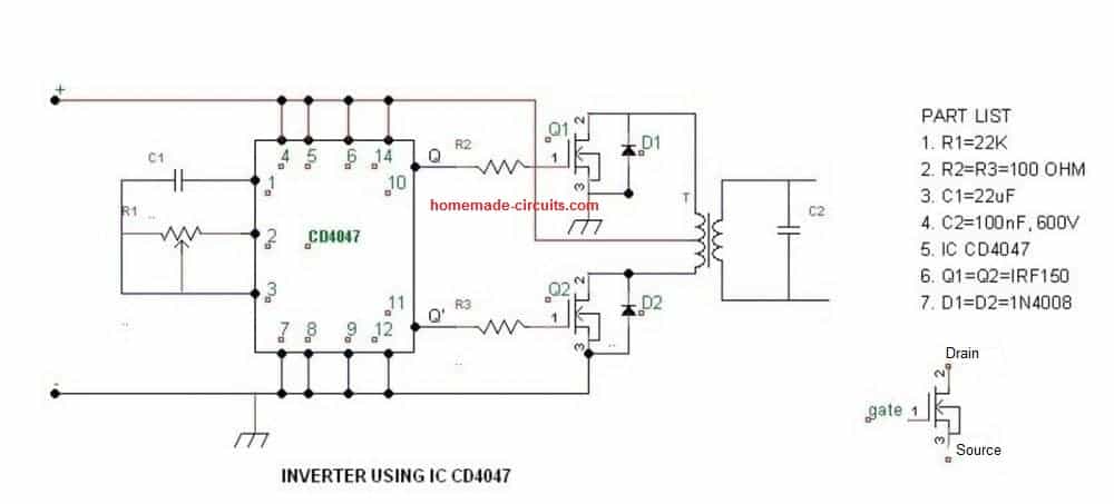
Making a Power Inverter using IC 4047
The IC is best suited for all types of inverter, converter, SMPS and timer applications.
One typical simple square wave inverter application using the IC 4047 can be witnessed below:
The formula for calculating the frequency or the RC components are:
- In Astable Mode →
tA = 4.4 × R × C
F = 1 / (4.4 × R × C) - In Monostable Mode →
tM = 2.48 × R × C
And this is from the official TI datasheet.

Comments
I think the capacitor is placed incorrectly. Can you tell me which side I should place anode and cathode?
which capacitor are you referring to? the pin#1 cap is rightly placed.
use a non-polar cap, and confirm that the IC is oscillates, using a headphone across the outputs, if the IC does not oscillate then the fets will quickly get damaged
Hello I have tested my circuit again with different MOSFETs and IC, results were same the output from the IC is 12v. When ever I connect the transformer connection between negative and source of MOSFETs gets broken please see the images in the link
Circuit https://imgur.com/gallery/4bfcj
This can never happen if everything’s correct in your circuit, I suspect your mosfets have problems or your mosfet connections
The way you have soldered looks very messy, you must clean the soldering with acetone or some cleaning agent, mosfets are extremely sensitive devices sand will burn with slightest inaccuracy. better use a PCB.
initially try with TIP122 instead of mosfets…that will give a clear idea regarding the proceedings, use a 10K base resistor if you are using this BJT
I checked the output using multimeter and the output is equal to input
with DC meter it should be 50% less than the supply, and using a frequency meter you must be able to read oscillations, which must change in response to varying of the R/C parts.
I built this circuit using cd4047BCN, irfp150n but it is not working when ever I connect it I get short circuit
check the IC output frequency without mosfets first, if the IC is working OK, then your mosfets could be faulty….
Hello sir, am just joining now, I want to build a pure sine wave inverter
what is the output waveform voltage(square wave) amplitude of the inverter which is to be appear across the transformer primary?
OK, will do, the reading will show around 50% value of the supply voltage, due to the 50% duty cycle from the IC.
sir,actually i was checking voltage across the drain terminals of mosfets as it is directly connected to the transformer primary.and yes we have checked the system with load also.
thank you so much sir for your answer,now i will check the voltage across drain and negative.
Tushar, across which points did you check the voltage? you must check it across the drain of the mosfet and the negative of the battery, or the across the drain/source leads.
but first you must connect a load at the output to confirm if the inverter was actually working in the way it is expected to work…if the load operates correctly, then you can go ahead with the voyage measurements.
ok sir . when we conncetd the syetsm as it is given in the circuit, the output was 220v (approx) thats okay…but the transformer input (primary) voltage was very less (in milivolts).so how can it step up to 220v as the voltage ratio is 12/220v…..so theoretically i think trns. primary voltage should be 12 v square wave because the output voltage is 220v square square wave ac.Am i right?
Is there any specific formula to calculate it?
220V if the trafo is rated at 12-0-12/220V
hello sir…. if the 12V battery is used,what will be the output voltage of inverter??
peak will depend on the battery and trafo specs and their compatibility
square wave
Hello sir
Can I make 3 phase inverter using IC CD4047 or any other IC.
Hello Paras, no it is not possible to make a 3 phase inverter using a 4047 IC…..special driver ICs will be required for this…I have posted many related article in this website, you may check them out through the search box
What is ouput of inverter or rating of inverter.
Hello sir
Can I make 3 phase inverter using this IC CD4047 or any other IC .
what is max. current capacity of IC CD4047
thank you
you mean at the output pinouts?….it might be around 10 to 20mA
hi so if i adjust the oscillator from cd4047 to be 50hz using the 1/8.8RC formula, i'll be feeding the same freq to the transformer input right? So at the output i'll get 230Vac 50Hz?
the frequency at each of the IC pins which are connected with the mosfets gates must be 50Hz…then your output will also be 50Hz
hi sir… can i used this cd4047 for DC CDI for motorcycle which this ic hv trigger pin for input pulse from magnet pulser.tx verry much
Hi Kribo, yes that's surely possible.
Sir,what are demerits of square wave inverter to home appliances?
Segun, it's the emission of noise….
Sir is the output sine or square wave.
It is square wave
sir
I have made an inverter with ic cd4047
which has 12v DC input . I want to increase the input voltage 12v to 24v what changes I have to done with the circuit???
You can implement the configuration as done for this design:
https://www.homemade-circuits.com/2014/11/48-v-inverter-circuit.html
Sir, this project uses PWM, high frequency is generated.
What type of transformer used: ferrite, siliceous iron (sheets EI)
jose, PWM is not used in the above design.
if ferrite core is used then the frequency must be set to around 30kHz, for iron core it can be 50 or 60Hz
Sir what is the total output wattage for this inverter above?
hello Sir! I want built a 100W solar inverter for project ….how can I increase the efficiency or what are the components that I may use for that purpose…can you suggest me with a circuit diagram
hello joydeep, efficiency normally depends on the overall transformer quality and the battery AH level, if you are able to get these two parameters optimally then your inverter would work with maximum efficiency.
Which type of relay i can use in this
Hello sir,
Can i use this circuit in 300 w inverter by using more MOSFET and using relay for charging the battery .
Hello Mayank,
you can make a 300 watt inverter by using IRF540 or any similar mosfet….more mosfets in parallel may not be required.
Hi sir,
Can you explain me what is oscillator and what is its work . I am new in electronics
Wasiq, PCB assembly will normally produce better results than breadboard, so your problem could be due to some hidden fault…..please check and compare each and every connection patiently and carefully, for troubleshooting the issue.
Sir i have designed inverter (12v dc to 220v ac) using IC4047, it's output is well enough when ever i test in bread board but when i do solding and wireing output voltage drop too much, whats the reason for that?.
kindly mail me in wasiqullah1@gmail.com
i will thankfull to you.
Hi Mayank,
an oscillator is a circuit which is able to produce alternate positive and negative voltages at its output at a given specified frequency