A very effective pure sine wave inverter circuit can be made using the IC 4047 and a couple IC 555 together with a few other passive components. I have explained the details below.
Introduction
In one of my previous posts I explained the main specifications and datasheet of the IC 4047 where I have explained how the IC could be configured into a simple inverter circuit without involving any external oscillator circuit.
In the next designs below we learn how a 4047 IC oscillator can be enhanced into a pure sine wave inverter circuit using a couple of additional ICs 555.
The IC 4047 section remains basically the same and is configured in its normal free running multivibrator mode with its output extended with the mosfet/transformer stage for the required 12V to the AC mains conversion.
How the IC 4047 Functions
The IC 4047 generates the usual square waves to the connected mosfets creating a mains output at the secondary of the transformer which is also in the form of square wave AC.
The integration of the two 555 IC to the above stage completely transforms the output into a pure sine wave AC. The following explanation reveals the secret behind the IC555 functioning for the above.
Audio/Video Representation
Converting a Square Wave 4047 Inverter into a Sine Wave Inverter
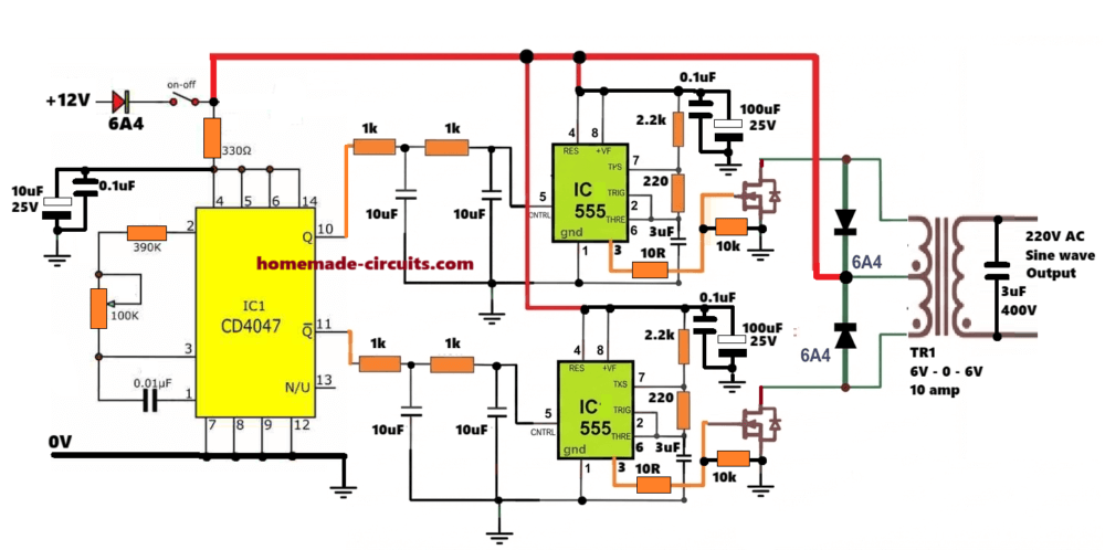
This circuit uses the 4047 IC and a couple of 555 PWM generator stages. Input is 12 Volts DC, output is 220 Volts AC sine wave.
Normally when people hear 4047 inverter, they think square wave. But here we are actually converting that basic 4047 square wave idea into a proper sine wave inverter.
The sine shape is created using PWM and then it is stepped up using a center-tapped transformer.
First thing is the power supply. The whole circuit runs from a 12 Volt battery. At the input we see a 6A4 diode. This is just for safety. If someone connects the battery in reverse by mistake then nothing burns…
Then we have a 330 ohm resistor and a few capacitors. These are just doing cleanup work. They smooth the supply and keep the control ICs stable.
Now comes the main frequency generator, the 4047 IC. This IC is working in astable mode and it is set to give 50 Hz square wave output. The frequency depends on 390K resistor, 100K preset and 0.01 uF capacitor.
That 100K preset is important. You can tweak it slowly and lock the frequency exactly at 50 Hz.
The nice thing about 4047 is that it gives two outputs across its pin 10 and pin 11. These two are exactly 180 degrees out of phase. That means… a perfect for push-pull inverter.
Now we do not send these square waves directly ahead. Each output first goes through a simple RC network. Just using 1K resistor and 10 uF capacitor.
These RC parts slowly round off the square waves and turn them into an acceptable smooth sine shape. Not pure sine, but good enough to control the next stage.
Now comes the most important section… the 555 ICs. We are using two 555 ICs, one for each half of the inverter.
These 555s are actually not oscillators.
They are working as PWM processors. The slow 50 Hz sine wave from the RC section is fed into pin 5 of each 555. Inside the 555, there is a fast triangle waveform created by its own timing parts.
The 555 compares the slow sine with the fast triangle.
Result?
At the output, we get sine-shaped PWM instead of square wave. That is the actual purpose of this circuit. Now this PWM output goes to the MOSFET gate through a 10K resistor.
The MOSFETs then switch the 12 Volt supply across the center-tapped transformer primary, following the PWM pattern exactly.
Since the PWM already looks like a sine wave, so the transformer does the remaining smoothing.
At the secondary side, we finally get a clean 220 Volts AC sine wave. We also have 6A4 diodes across the transformer winding. These are there to handle spikes and back EMF and safeguard the MOSFETs and the ICs from transformer back EMFs.
At the output side, you can see a 3 uF / 400 Volt capacitor. This capacitor removes the high-frequency PWM leftovers. After this, the sine wave becomes much smoother and safe even for sensitive loads.
So overall, this inverter is simple, practical and very effective. Perfect for DIY guys who want sine wave output without complicated ICs.
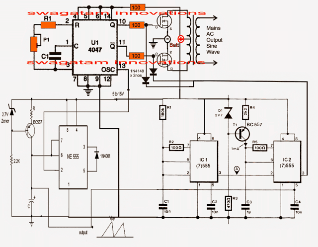
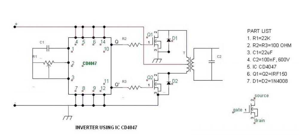
Another Version, again Using IC 555 for the PWM Processing
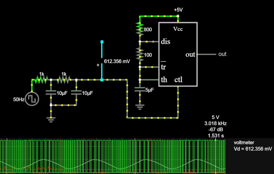
Referring to the next below shown IC 4047 pure sine wave inverter circuit (also designed by me), we can see two identical IC 555 stages, wherein the left section functions as a current controlled sawtooth generator while the right hand side section as a current controlled PWM generator.
The triggering of both the 555 ICs are derived from the oscillator output readily available across pin#13 of IC 4047. This frequency would be 100Hz if the inverter is intended for 50Hz operations, and 120Hz for 60Hz applications.
Using IC 555 for the PWM Generation
The left 555 section generates a constant sawtooth wave across its capacitor which is fed to the modulating input of the IC2 555 where this sawtooth signal is compared with the high frequency signal from pin3 of IC1 555 creating the required pure sine wave equivalent PWM at pin#3 of 555 IC2.
The above PWM is directly applied to the gates of the mosfets. so that the square pulses here generated through pin10/11 of IC4047 gets chopped and "carved" as per the applied PWMs.
The resulting output to the transformer also causes a pure sine wave to be stepped up at the mains AC secondary output of the transformer.
The formula for calculating R1, C1 is given in this article which also tells us about the pinout details of the IC 4047
For the NE555 stage C may be selected near 1uF and R as 1K.
Assumed output waveform
More info on how to use IC 555 for generating PWM
An RMS adjustment could be added to the above design by introducing a pot voltage divider network across pin5 and the triangle source input, as shown below, the design also includes buffer transistors for improving mosfet behavior
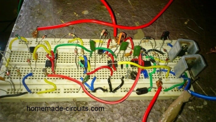
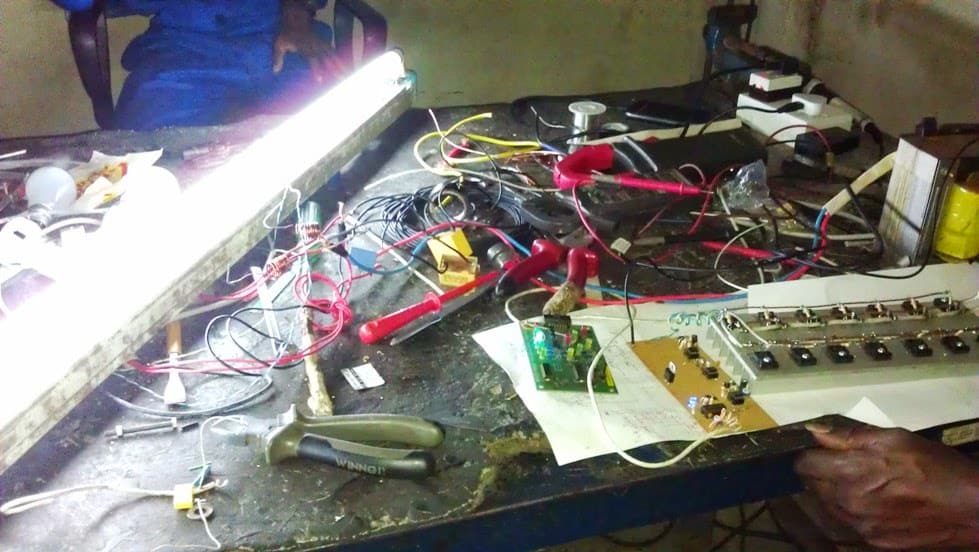
The above pure sine wave inverter design was successfully tested by Mr. Arun Dev, who is one of the avid readers of this blog and an intense electronic hobbyist. The following images sent by him prove his efforts for the same.
More Feedback
Inspiring response received from Mr. Arun regarding the above IC 4047 inverter results:
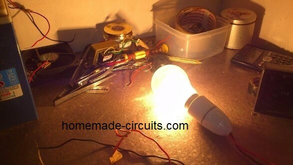
After completing this circuit, the result was amazing. I got full wattage by the 100 W bulb. Couldn't believe my eyes.
The only difference i had made in this design was replacing the 180 K in the second 555 with a 220 K pot to adjust the frequencies accurately.
This time the result was fruitful in all respects... On adjusting the pot, i could get a non disturbing non flickering full wattage glow in the bulb, also the 230/15 V transformer connected as the load gave a frequency in between 50 and 60 ( say 52 Hz ).
The pot was adjusted gently to get a high frequency ( say 2 Khz ) output from pin#3 of second ic 555. The CD4047 section better calibrated to get 52 Hz at the two output terminals....
Also I am facing a simple problem. I have used IRF3205 mosfets at the output stage. I forgot to connect the safety diodes across the drain terminals of each mosfets...
So when I had tried connecting an another load ( say table fan ) in parallel to the given load ( 100 W bulb ), the glow of the bulb also the speed of the fan was reduced a little and one of the MOSFET was blown due to the absence of the diode.
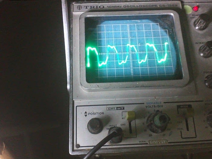
The above 4047 sine wave inverter circuit was also tried successfully by Mr. Daniel Adusie (biannz), who is a regular visitor of this blog, and a hardworking electronic enthusiast. Here are the images sent by him verifying the results:
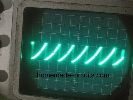
Sawtooth Waveform Oscilloscope Output
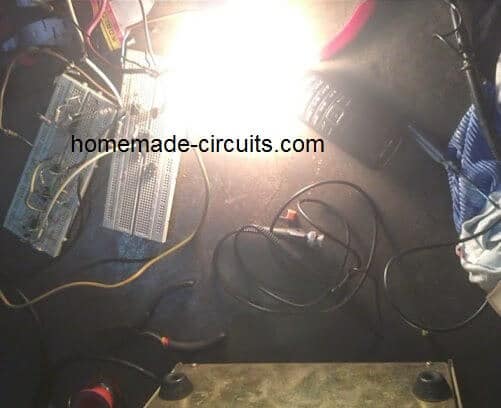
Illuminating a 100 Watt Test Bulb
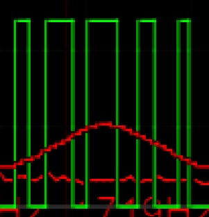
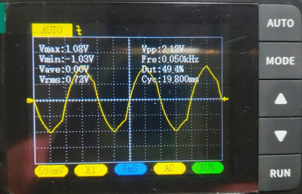
The following images show the modified waveforms at the output of the transformer as captured by Mr. Daniel Adusie after connecting a 0.22uF/400V capacitor and a suitable load.
The waveforms are somewhat trapezoidal and are far better than a square wave which clearly shows the impressive effects of the PWM processing created by the IC555 stages.
The waveforms could be probably even further smoothened by adding an inductor along with the capacitor.
Showing an near Sinewave Oscilloscope Trace after PWM Filtration
Interesting feedback received from Mr. Johnson Isaac who is one of the dedicated readers of this blog:
Good day
In your post, Pure Sine Wave Inverter using 4047, in the second I.c stage (ic.1) you used 100 ohms resistor in between pin 7 and 6.,
Is that correct? I use to think an astable multivibrator using 555 pin configuration should have the 100 ohms between pin 7 and 6. Also, the 180k variable between pin 8(+) and pin 7. Pls check the pin connection and correct me pls. Because it oscillate sometimes and it doesn't sometimes also. Thanks,
Isaac Johnson
Solving the Circuit Issue:
In my opinion, for a better response you can try connecting an additional 1k resistor across the 100 ohm outer end and pin6/2 of IC1
Johnson:
Thank you very much for your response. I actually constructed the inverter you gave in your blog and it worked.
Though I don't have an oscilloscope to observe the output waveform BUT I bet readers its a good one cos it operated a fluorescent tube lamp in which any modified or pwm inverter can't power on.
See the picture sir. But my challenge now is when I add load, the output flickers sometimes. But am happy its a sine wave.
Video Test Waveform
Simplifying the above Concept
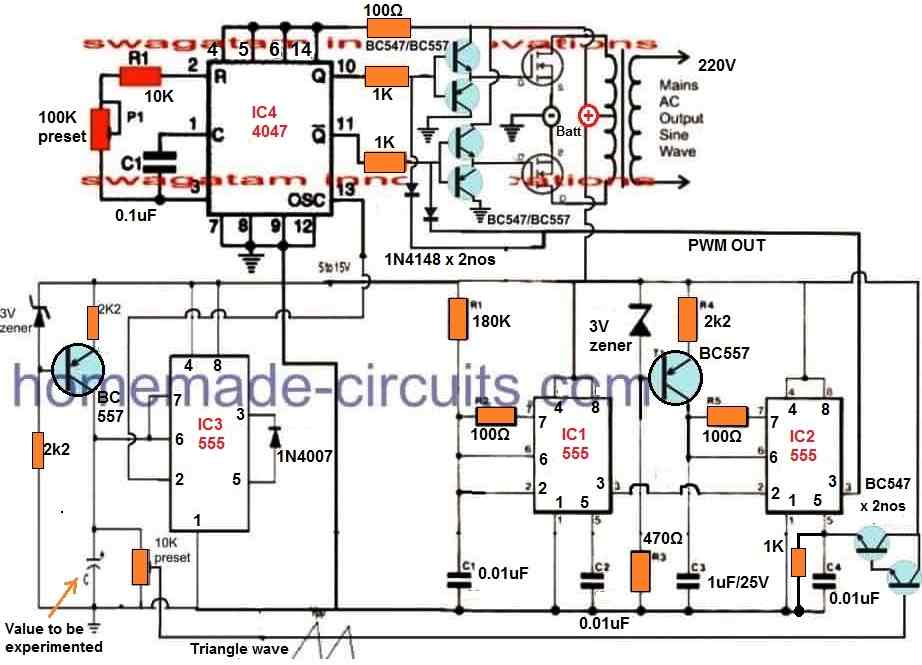
The above explained IC 4047 pure sine wave inverter can be actually simplified greatly by eliminating two IC 555 configurations from the design.
The basic idea is to produce a synchronized sine PWM output for chopping the MOSFET switching so that this SPWM waveform is replicated at the output of the transformer and is transformed into a pure sine waveform. The complete circuit diagram can be seen in the following diagram:

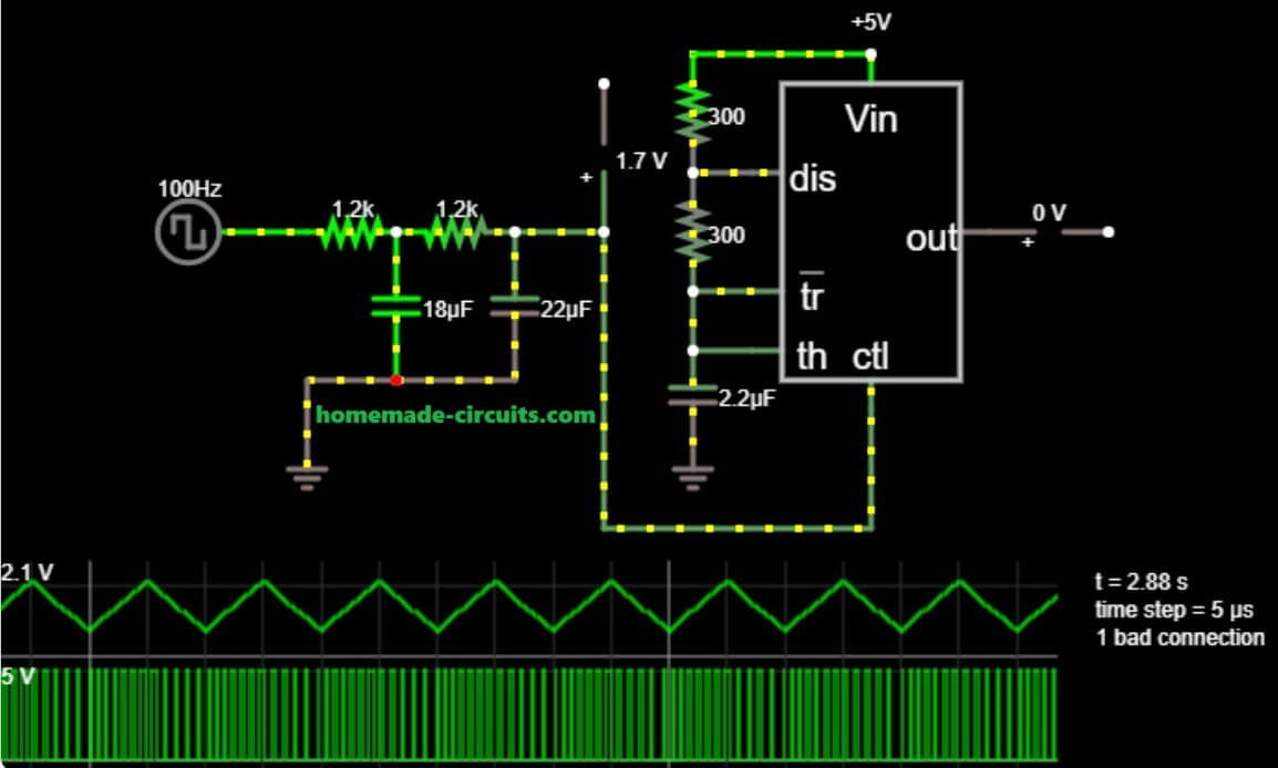
In this simplified design, we yet again exploit the pin#13 square wave output from the IC 4047 and convert it into triangle waves. This triangle wave is then used to modulate the PWM output of a IC 555 astable to create the required synchronized SPWM for chopping the MOSFET gates.
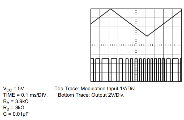
Simulation Results for the SPWM output
The following image shows the simulation results of the 555 SPWM section of the above circuit, which looks like a good SPWM output and should be able to replicate a good AC 220V sine wave at the output of the transformer.

How SPWM is Generated from Pin 5 of IC 555 in this Circuit
Now first we have to understand that this is a simple IC 555 timer circuit connected in astable mode. We know that IC 555 has many pins but here the most important part is pin number 5, which is called control voltage pin.
Then we see a square wave generator working at 100 Hz (coming from pin#13 of IC 4047) connected through resistors and capacitors, that is 1.2k resistors and 18 microfarad, 22 microfarad capacitors.
These components together make a triangle wave signal. We know that square wave goes in and because of the RC charging and discharging, now a smooth triangle wave appears at the junction point before control voltage pin 5 of IC 555.
Then we see that the triangle wave amplitude is around 0 volts to about 2 volts and this triangle waveform keeps rising and falling slowly with time at 100 Hz frequency.
Now this triangle wave is directly applied to control pin 5 of the IC 555. Since pin 5 controls the internal comparators inside IC 555, that affects how the IC behaves.
Because of this, the IC 555 produces an output PWM signal from pin number 3 and the special thing is the pulse width of this output is not fixed but keeps changing smoothly depending on the triangle wave amplitude.
So when the triangle wave voltage is higher, then pulse width of the output becomes wider and when the triangle voltage is lower, then pulse width becomes narrower.
This process is how the sinusoidal pulse width modulation happens or we can say approximate SPWM is generated. The upper part of the graph shows the triangle waveform at around 100 Hz and the lower graph shows high frequency pulses with varying pulse width – this is the SPWM.
Now it is important to know that this is not a pure sine SPWM, but a simple triangle modulated PWM. If we want true sinusoidal SPWM then we should compare a sine wave and a triangle wave using a comparator circuit. But in this simple circuit, only the triangle wave is applied to pin 5, so it gives us approximate SPWM output.
Then we can use this kind of SPWM for applications like inverters where we need to simulate AC power using switching pulses. The key idea is that smooth variation of pulse width follows the triangle waveform shape, and this is very useful for power electronics.
That is how the whole process works. We generate triangle wave then apply to control voltage pin 5 then IC555 produces PWM output at pin 3 with varying pulse width according to triangle shape. This is called SPWM.
Next, finally when this SPWM is applied to the bases of the inverter MOSFET driver BJTs, the MOSFETs switch the transformer winding with the exact pattern of the SPWM, consequently forcing an SPWM waveform at the output of the transformer.
This can be further filtered and converted into a pure sine wave like waveform simply by adding a 3uF/400V PPC capacitor across the secondary wires of the transformer...
Sine Wave instead of Triangle wave
Please note that here we are using triangle waves for replicating the output sine wave which may not be a perfectly pure sine wave. So ideally, the triangle waves at pin#5 of IC 555 must be replaced with a sine wave, and this can be simply done by adding another layer of RC network with the existing 2 stage RC network, to make it a 3 stage RC filter.
Expected Output:
With these values our circuit will do a moderate job of cutting down those harmonics, and what we will end up with is a rough sine wave that has quite a bit of distortion. If you want to get things just right, you can tweak the values of the resistors or capacitors a little bit to fine-tune that waveform.
Another Simpler Looking Options
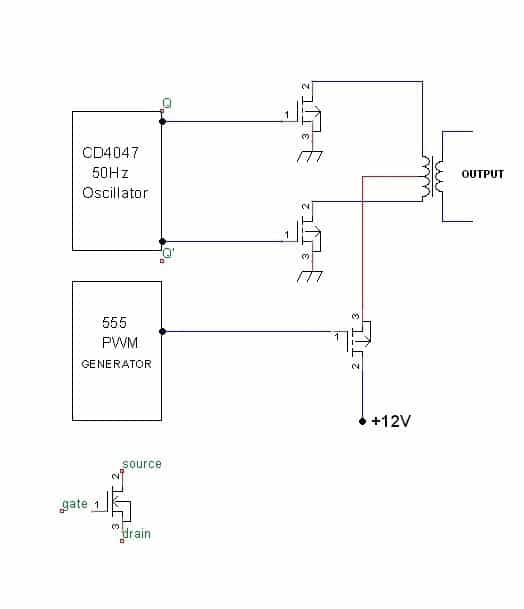
The following concept discuses a rather simpler method of modifying an ordinary square wave inverter using IC 4047 into a sine wave inverter through PWM technology. The idea was requested by Mr. Philip
Technical Specifications
I hope that i am not going to be a bother, but I need some advice with a PWM-controlled modified sine wave inverter I am designing so I want to seek your expert opinion.
This simple design is tentative, I haven't implemented it yet but I would like you to take a look at it and tell me what you think.
Also I want you to help answer some questions which I have not been able to find answers to.
I have taken the liberty of attaching an image of a quasi-block diagram of my tentative design for your consideration.
Please help me out. In the diagram, the IC CD4047 in the inverter is responsible for generating square wave pulses at 50Hz which will be used to alternately switch on MOSFETS Q1 and Q2.
The PWM circuit will be based on IC NE555 and its output will be applied to the gate of Q3 so that Q3 will provide the PWM. Besides this, I have two questions.
First, can I use square waves for the PWM pulses? Second, what is the relationship between PWM frequency and supply frequency? What PWM frequency should I use for a 50Hz inverter output?
I hope that this design is feasible, I think it is feasible, but I want your expert opinion before I commit scarce resources to implement the design.
Looking forward to hearing from you sir!
Sincerely, Philip
Solving the Circuit Request
The configuration shown in the second figure above would work only if the center tap mosfet drain/source pins are swapped and N-channel mosfets are used for the 4047 inverter oscillator output, as shown below:
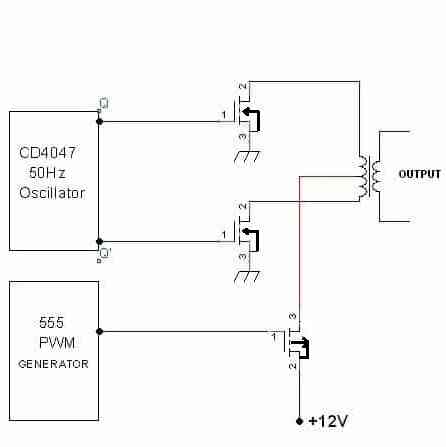
The PWM section should be built as I have explained in this article:
The PWM transforms the flat square waves into a modified square wave by chopping them into smaller calculated sections such that the overall RMS of the waveform becomes as close as possible to an actual sine counterpart, yet maintaining the peak level equal to the actual square wave input. The concept may be learned in details here:
However the above transformation does not help to eliminate the harmonics.
The PWM frequency will be always in the form of chopped square waves.
The PWM frequency is immaterial and may be of any high value, preferably in kHz.
How to Add Feedback Voltage Control to a 4047 IC Inverter
In this section we will discuss how to add an automatic feedback voltage control to a 4047 IC based inverter circuit.
If you don't want to read the whole explanation, you can watch the following video instead:
This type of feedback network is intended to ensure that the AC output voltage from the inverter never exceeds a predetermined safe value. For example, using this automatic feedback control, a 220 Volt inverter circuit output could be restricted to maximum 230V AC level, which may be safe for most 220 Volts appliances.
For a 120 Volt inverter system, this feedback network could be adjusted to restrict the output AC to a maximum of 115 Volts AC, which may be safe for most 110 Volt appliances.
How the Feedback Circuit Works
Now let's understand how the simple feedback network is designed to work, by referring to the following circuit diagram:
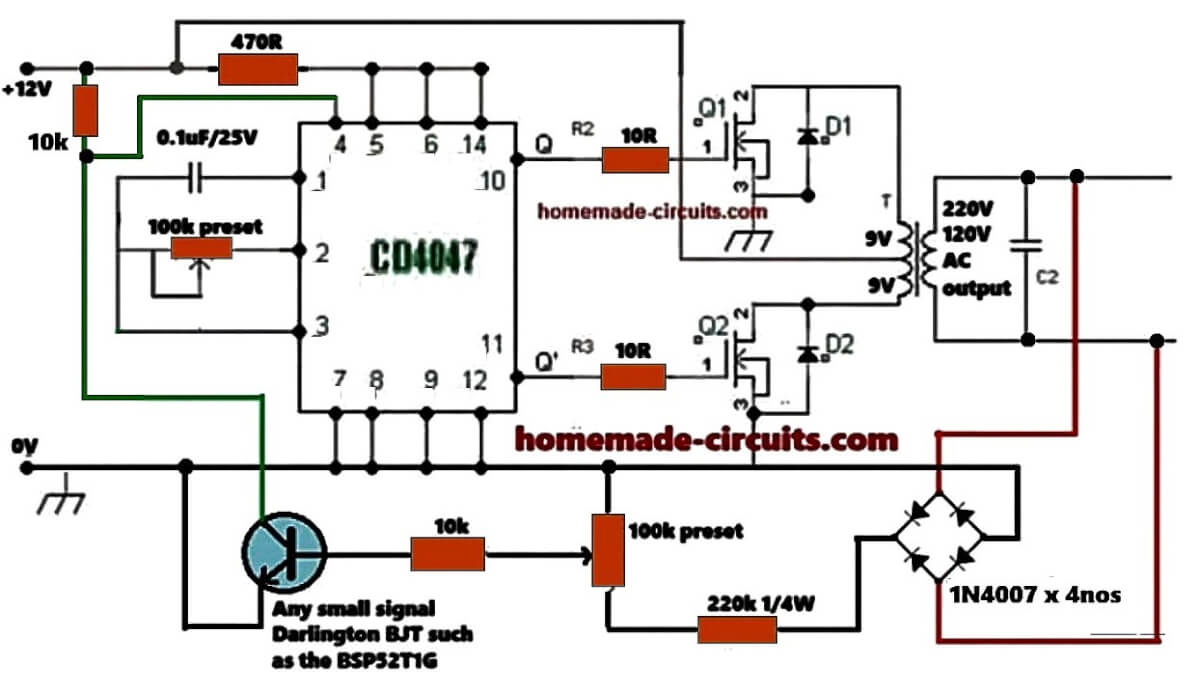
The mains AC voltage from the inverter transformer secondary is first converted to a DC voltage using a bridge rectifier.
This bridge rectifier is built using 4 numbers of 1N4148 diodes.
The DC 220 Volts output from the bridge rectifier is applied to an adjustable voltage divider network built using a 220 k resistor and a 100 k preset or trimpot.
The 100 k preset is carefully adjusted such that its central wiper terminal generates around 1.2 volts in response to an input AC voltage which is considered high, and needs to be restricted.
Let's say, the input AC needs to be restricted at around 270 Volts, then the 100 k preset may be adjusted so that its wiper terminal generates a proportional DC voltage level of 1.2 Volts.
We select a 1.2 Volt output because this is the equivalent DC level required to just switch ON the attached BJT device.
That means, whenever the inverter output AC voltage tries to exceed the 270 Volts mark, it causes the BJT to turn ON and become conductive.
When the BJT conducts, it starts grounding the CT pin of the IC 4047.
Since the RC network associated with the CT and the RT pinouts of the IC determines the output frequency and PWM, the grounding of the CT pin instantly causes the output PWM and frequency to nullify, which in turn causes the output AC voltage to dip.
When this happens, the feedback voltage to the BJT also drops proportionately until the BJT is turned off. In this situation the IC output PWM is restored back to its previous form, and if the output voltage continues to rise, it yet again activates the BJT via the feedback network, and this feedback on off cycle keeps repeating rapidly, ensuring that the output AC is not able to rise above the set threshold, which is 270 volts in our example.
This concludes our feedback control circuit explanation, now let's try to understand how this feedback circuit can be setup prior to integrating it with the inverter circuit.
How to Setup
The next diagram below shows the isolated feedback circuit, which can be set up by implementing the following steps, before interfacing it with your inverter circuit:
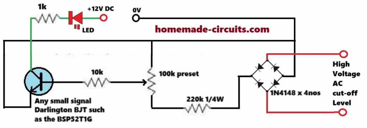
Initially keep the 100k preset's wiper arm fully towards the ground side of the DC supply.
Now, switch ON the 12 DC supply and then switch ON the AC supply to the bridge rectifier whose voltage level is around the desired high cut-off limit.
Next, slowly adjust the preset using a well insulated screw driver, until the LED just begins to illuminate.
To confirm the results, try varying the input AC voltage around the cut-off threshold and watch the LED turn on and off at the thresholds. Although the cut-off may not be too sharp, yet it will do the job of the intended output voltage control of the inverter quite well.
That's it! This simple procedure should be enough to complete the setting up of the feedback circuit.
After this, make sure to seal the preset adjustment with some super glue.
So, this concludes our explanation on a feedback circuit for the 4047 inverter.


Questions & Answers
please (1) how can I connect the 100k PRESET ,it has three pin terminal how can I connect the three terminal. (2) IC 4047 ,pin 13 where is it connected to
Use only two terminals, the center terminal ad any one of the outer terminals…
Pin13 goes to the 555 pwm processor…
Hi Swagatam,
Why not use a crystal to have a better stabilized frequency? I once made a 50Hz square wave inverter using a 3.2768MHz crystal, a 4060 and a 4027 ICs. At least connected appliances fitted with a clock keep time, motors keep correct speed. The last inverter I built this way was a small, approximate sine wave, one made so that I can use some kinds of 50Hz European appliances in North America where only 60Hz supply is available. This included a 50Hz turntable and a tape recorder that requires precise frequency to avoid wow and flutter.
Thanks Marc,
Yes definitely we can improve the frequency stability by using a crystal for such inverter circuits, and using crystal is always recommended for inverter designs so that they can supply a fixed frequency to all critical loads and devices…
please why was 100hz used, is it statutory, can higher frequency be used, what is an optimal range to use?
Hi, when pin10 and pin11 are set to generate 50Hz, then Pin13 will generate 100 Hz…
O CI CD4047 está sendo usado para gerar uma saída de 60Hz nos pinos 10 e 11. Os pinos 4,5,6 e 14 estão com +12V. Os pinos 7,8,9 e 12 estão com OV. O pino 1 vai ao C1 com 100nf e o seu outro polo vai ao pino 3. O pino 2 vai ao R1 33K em série com R2 4K7 em série com R3 180R este último da série vai ao pino 3. Não tenho como medir. Consegui os 60Hz no pino 10? Se não houver conseguido me oriente para colocar um ou até três resistores fixos. Atenciosamente José Paulo
Você pode consultar este artigo, que explica claramente como calcular a frequência do CI CD4047 usando resistor e capacitor, e também como ajustar para 60Hz:
https://www.homemade-circuits.com/ic-4047-calculator-frequency-and-pwm/
Este material pode ajudar mesmo sem instrumentos de medição.
Good day, Engr. can you assist me with the Gerber file of Spwm inverter circuit so I can use for my PCB.
God bless you.
Sorry Offor, Gerber files is not available for this project..God bless you too…
Hello Swag,


I tried the circuit according to latest schematic as updated by you
I got near sine waveform as per oscilloscope image attached
please tell if I can run induction motor on this waveform or need to further improve the waveform
Thank you Sachin,

It looks good. At what point are you getting this waveform? I think we should check it at the output of the transformer.
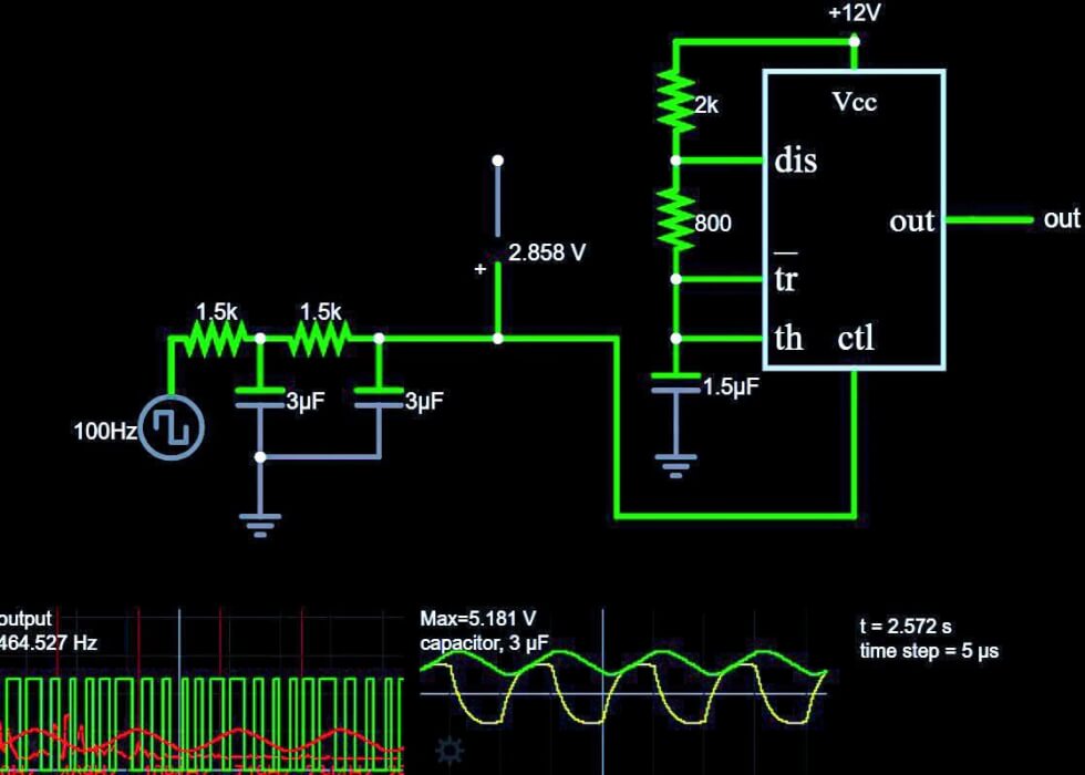
However, I simulated the SPWM section again, and found some other part values which gave better sine output:
Here’s simulation text code, which you can paste on the simulator provided in this website.
$ 1 0.000005 4.818269829109882 56 5 50 5e-11
165 384 96 400 96 0 4.999999950000001
R 448 64 448 48 0 0 40 5 0 0 0.5
O 512 160 560 160 0 0
w 384 128 352 128 0
r 352 128 352 64 0 2000
w 352 64 448 64 0
w 352 224 384 224 0
c 352 224 352 272 4 5.000000000000001e-7 0.8127020048389597 0.001 0
g 352 272 352 288 0 0
w 352 192 352 224 0
w 352 192 384 192 0
r 352 128 352 192 0 100
r 80 224 128 224 0 1500
r 128 224 192 224 0 1500
c 128 224 128 288 4 0.0000022 -3.0692257316279603 0.001 0
c 192 224 192 288 4 0.0000022 1.4138956572327113 0.001 0
w 192 288 128 288 0
g 128 288 128 320 0 0
R 80 224 80 272 0 2 100 12 0 0 0.5
w 256 224 320 224 0
w 320 224 320 320 0
w 448 256 448 320 0
p 256 224 256 128 1 0 0 0
w 256 224 192 224 0
w 320 320 448 320 0
o 2 32 0 5134 5 0.00009765625 0 1 output
o 22 32 0 4098 10 0.1 1 1
Can the rc resistor use a 1k resistor and a 33μf capacitor?
What will be the input frequency? That won’t work according to me.
You can simulate it here:
https://www.homemade-circuits.com/simulator/circuitjs.html
50hz use a 600va ct 7v transformer
33uF for the RC circuit will not work, here’s what works, with 7V, 50Hz:
yes Sir,
this is waveform at output of transformer after using 3uF 440v filter capacitor
OK, Great, then you can definitely use an induction motor with this AC. If possible please also consider testing the new SPWM configuration parts which I suggested in the last reply…
Hi Swag,
I get this output waveform at transformer after using 3uF filter capacitor.
I tried many different values of resistors and capacitors and this is the best I could achieve.
My final values are
resistor between pin 7&8 of IC 555 is 2.2k, also resistor between pin 6&7 2.2k
capacitor between pin 6& ground is 1uF or 2uF both work fine
Thank you Sachin, for updating the results…
But no it is not looking good…it is looking more like triangle waves, not sine waves.
I think your previous results were better.
So I think you should tweak the previous settings and check whether the previous sine waveform can be improved further or not…
please from Mr Bangar’s first post, and your latest 555 circuit pwm frequency output from calculation, over 1khz, is this frequency in line as you have repeatedly said for laminated iron core, it should be less than 400hz.
You can use the following pwm configuration for an iron core transformer:
Yes Sir,
I will definitely test the new schematic and share results with you. Infact, I am going to test many different circuits from your website and sharing results with you
Sure, no problem Sachin, All the best to you…
Hello Mr Swag, you said “If you want to get things just right, you can tweak the values of the resistors or capacitors a little bit to fine-tune that waveform.”
I have tried your recommendations for CX and cy, Its harmonics was still high.
How best to perfect the waveform?
Hello Bay,
What kind of waveform are you getting after the optimizations? You can try simulating the results in the following simulator:
https://www.homemade-circuits.com/circuit-simulator/
Thank you Mr. Swagatam for the article that really helped me in terms of knowledge of electronics applications.
You are most welcome Sumerta, I am glad you found my articles helpful.
Good day sir, thanks for your articles.
I have been trying to tweak various values of CX, cy ranging from pf to nf but the waveform was still sawtooth, please is there anything to do to improve the quality.
However, the inverter was able to power what ordinary modified square wave inverter could not power.
Thanks sir, I appreciate.
Good day Seun,
In the shown RC passive integrator circuit, the voltage across CX should be a sawtooth and the voltage across CY should be transformed to sine wave. It is a standard RC integrator circuit and should produce the intended results.
You must try try adjusting the resistors also.
Or you can try calculating the parameters using any online software, or online formulas and check the results.
Ok sir, thanks for the enlightenments. please what values and parameters to use, I couldn’t get any online calculator to use, please assist Me
Seun, I have updated the calculations in the above article for the Cx, Cy values, please check it out….
Thanks for your input. please what is the effect of crude sine wave and it’s meaning. is there anyway to enhance it?
It is not too crucial, even with crude sine at pin#5 of the IC 555, the inverter output will produce a decent sine wave provided it is appropriately filtered through capacitors at the output. You can use 3uF/400V PPC capacitors at the inverter output.
Thanks sir for your guide, I noticed the frequency generator produced 1.4Khz with R1 4,7k and R2 47k at the 555 timer does it have any implication?
Seun, 1.4kHz is high for an iron core transformer, it should not be more than 300 Hz, so please adjust the capacitor value accordingly.
The duty cycle will control the output voltage.