I have explained comprehensively how to build a boost converter circuit for converting a low level DC voltage inputs to a higher level DC voltage outputs. I have furnished all the required calculations s that you can design a customized boost converter circuit.
A Practical Boost Converter Circuit Design using IC 555
This simple circuit is built using an IC 555 circuit for boosting USB 5V to 24V, or any other desired level. The same design can be used for boosting a 3.7 V to 24 V from a Li-Ion cell.
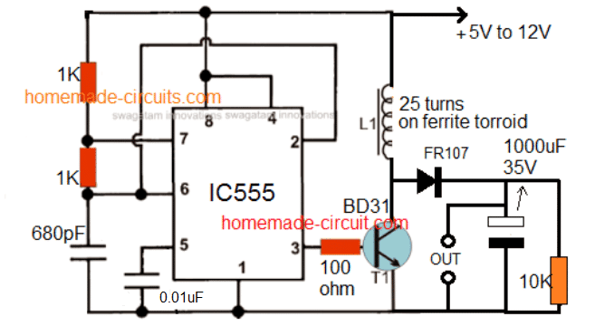
Let's assume we have the following parameters required for the above circuit:
Important Parameters:
- Input Voltage (Vin): 5V
- Output Voltage (Vout): 24V
- Output Current (Iout): 1A
- Switching Frequency (f): 50 kHz
Calculating the Part Values
Step 1: Output Power
Pout = Vout * Iout = 24V * 1A = 24WEfficiency (η) = 85%
Pin = Pout / η = 24 / 0.85 ≈ 28.2WInput Current (Iin) = Pin / Vin = 28.2 / 5 ≈ 5.64AStep 2: Inductor Selection
Inductance (L) = (Vin * D) / (f * ΔI)D = 1 - (Vin / Vout) = 1 - (5 / 24) ≈ 0.79Ripple Current (ΔI) = 0.4 * Iin = 0.4 * 5.64 ≈ 2.26AL = (5 * 0.79) / (50000 * 2.26) ≈ 35µHChoose an inductor with L = 35µH, capable of handling at least 6A peak current.
Step 3: Diode Selection
Reverse Voltage: ≥ Vout = 24VForward Current: ≥ Iout = 1AChoose a Schottky diode, such as MBR360 (60V, 3A).
Step 4: Capacitor Selection
Output Capacitor (C) = (Iout * D) / (f * ΔV)Assume Ripple Voltage (ΔV) = 1V:
C = (1 * 0.79) / (50000 * 1) ≈ 16µFChoose a low-ESR electrolytic capacitor, such as 100µF, 35V.
Step 5: Resistor Selection for 555 Timer
Frequency (f) = 1.44 / ((R1 + 2R2) * C1)Assume C1 = 0.01µF:
R1 + 2R2 = 1.44 / (50 * 103 * 0.01 * 10-6) = 2.88kΩSet R1 = 1kΩ, then 2R2 = 1.88kΩ, so R2 = 940Ω.
Use standard values: R1 = 1kΩ, R2 = 1kΩ.
Finalized Part values for the above 555 boost Converter Circuit
L1: 35µH, 6A
D1: MBR360 (60V, 3A Schottky)
Cout: 100µF, 35V (low ESR)
R1 & R2: 1kΩ each
C1 (timing): 0.01µF
T1 (switch): BD31 or better NPN transistor capable of 6A or a MOSFET (e.g., IRF540N)
Construction Steps (How to Assemble)
Step 1: Build the Oscillator Circuit
Assemble the 555 timer circuit on a breadboard or PCB.
Use the formula for the 555 timer frequency:
f = 1.44 / ((R1 + 2R2) * C1)Select the appropriate values for R1, R2, and C1 to achieve the desired switching frequency (e.g50 kHz).
Connect the output of the 555 timer (pin 3) to the base or the gate of the switching transistor/MOSFET through the resistor (e.g 100Ω).
Step 2: Connect the Inductor and Switching Transistor
Solder the inductor (e.g.35µH) in series with the input voltage and the collector (or drain) of the switching transistor.
Connect the emitter (or source) of the transistor to ground.
Step 3: Add the Diode
Solder the Schottky diode (e.g MBR360) between the inductor and the output capacitor.
Connect the cathode of the diode to the positive terminal of the output capacitor.
Step 4: Connect the Output Capacitor
Add an electrolytic capacitor (e.g., 100µF 35V) across the output terminals for to smooth out the boosted DC voltage.
Step 5: Feedback/Control (Optional)
For adjustable output voltage you can include a feedback circuit with a variable resistor (potentiometer) to adjust the duty cycle of the PWM signal.
Step 6: Add Input and Output Terminals
Solder the connectors or terminals for the input voltage (Vin) and output voltage (Vout).
Step 7: Verify Connections
Double-check all the connections to ensure that there are no shorts or loose connections.
Testing the Circuit
Connect the 5V DC power supply to the input terminals.
Measure the output voltage using the multimeter to ensure that it reaches the desired value (e.g.,, 24V).
Adjust the duty cycle (if applicable,) to fine-tune the output voltage.
Connect the load (e.g, a resistor or a small motor) to the output and measure the current.
Assembly Tips
Use the heat sink for the transistor or MOSFET to dissipate the heat during the operation.
Keep the connections between the inductor, switch, diode, and the capacitor as short as possible to minimize the losses.
Use the printed circuit board (PCB) for getting a robust and reliable assembly.
Adding a Feedback
The above circuit can be regulated with a feedback as shown below:
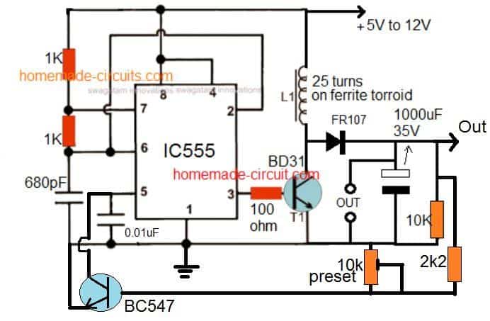
The idea looks quite straightforward. IC 555 is configured as an astable multivibrator whose frequency is decided by the values of resistors and capacitor at pin#7 and pin#6/2.
This frequency is applied to the base of a driver transistor TIP31 (incorrectly shown as BD31).
The transistor oscillates at the same frequency and forces supply current to oscillate within the connected inductor with the same frequency.
The selected frequency saturates the coil and boosts the voltage across it to a greater amplitude which is measured to be around 24V.
This value can be tweaked to even higher levels by modifying the turns of the inductor and the frequency of the IC .
Video Demonstration for IC 555 Boost Converter circuit
How a Boost Converter Works (Theoretical Analysis)
A boost converter is a kind of SMPS or switch mode power supply which fundamentally works with two active semiconductors (transistor and diode) and with a minimum of one passive component in the form of a capacitor or an inductor or both for greater efficiency.
The inductor here basically is used for stepping up the voltage and the capacitor is introduced for filtering the switching fluctuations and for reducing current ripples at the output of the converter.
The input power supply which may be required to be boosted or stepped up could be acquired from any suitable DC source such as batteries, solar panels, motor based generators etc.
Operating Principle
The inductor in a boost converter plays the important of stepping up the input voltage.
The crucial aspect which becomes responsible for activating the boost voltage from an inductor is due to its inherent property of resisting or opposing a suddenly induced current across it, and due to its response to this with a creation of magnetic field and subsequently destroying of the magnetic field. The destroying leads to the releasing of the stored energy.
This above process results in the storing of the current in the inductor and kicking back this stored current across the output in the form of back EMF.
A relay transistor driver circuit can be considered a great example of a boost converter circuit. The flyback diode connected across the relay is introduced to short circuit the reverse back EMFs from the relay coil and to protect the transistor whenever it switches OFF.
If this diode is removed and a diode capacitor rectifier is connected across the transistor's collector/emitter, the boosted voltage from the relay coil can be collected across this capacitor.
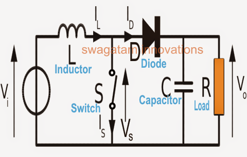
The process in a boost converter design results in an output voltage that’s always higher than the input voltage.
Boost Converter Configuration
Referring to the following figure, we can see a standard boost converter configuration, the working pattern may be understood as given under:
When the shown device (which could be any standard power BJT or a mosfet) is switched ON, current from the input supply enters the inductor and flows clockwise through the transistor to complete the cycle at the negative end of the input supply.

During the above process the inductor experiences a sudden introduction of current across itself and tries to resist the influx, which results in the storing of some amount of the current in it through the generation of a magnetic field.
At the next subsequent sequence, when the transistor is switched OFF, the conduction of current breaks, yet again forcing a sudden change in the current level across the inductor.
The inductor responds to this by kicking back or releasing the stored current. Since the transistor is in the OFF position, this energy finds its path through the diode D and across the shown output terminals in the form of a back EMF voltage.

The inductor performs this by destroying the magnetic field which was earlier created in it while the transistor was in the switch ON mode.
However, the above process of releasing energy is implemented with an opposite polarity, such that the input supply voltage now becomes in series with the inductor back emf voltage. And as we all know that when supply sources join in series their net voltage adds up to produce a bigger combined outcome.
The same happens in a boost converter during the inductor discharge mode, producing an output which may be the combined result of the inductor back EMF voltage and the existing supply voltage, as shown the diagram above
This combined voltage results in a boosted output or a stepped up output which finds its path through the diode D and the across capacitor C to ultimately reach the connected load.
The capacitor C plays quite an important role here, during the inductor discharge mode the capacitor C stores the released combined energy in it, and during the next phase when the transistor switches OFF again and the inductor is in the storing mode, the capacitor C tries to maintain the equilibrium by supplying its own stored energy to the load. See the figure below.

This ensures a relatively steady voltage for the connected load which is able to acquire power during both the ON, and OFF periods of the transistor.
If C is not included then this feature is cancelled resulting in a lower power for the load and lower efficiency rate.
The above explained process continues as the transistor is switched ON/OFF at a given frequency, sustaining the boost conversion effect.
Modes of Operation
A boost converter may be primarily operated in two modes: the continuous mode, and the discontinuous mode.
In continuous mode, the inductor current is never allowed to reach zero during its discharging process (while the transistor is switched OFF).
This happens when the ON/OFF time of the transistor is dimensioned in such a way that the inductor is always connected back quickly with the input supply through the switched ON transistor, before it’s able to get completely discharged across the load and the capacitor C.
This allows the inductor to consistently produce the boost voltage at an efficient rate.
In the discontinuous mode, the transistor switch ON timing may be so wide apart that the inductor may be allowed to get discharged fully and stay inactive in between the switch ON periods of the transistor, creating huge ripple voltages across the load and the capacitor C.
This could make the output less efficient and with more fluctuations.
The best approach is to calculate the ON/OFF time of the transistor which yields maximum stable voltage across the output, meaning we need to make sure that the inductor is optimally switched such that it’s neither switched ON too quickly which might not allow it to discharge optimally, and nor switch it ON very late which might drain it an inefficient point.
Calculating, Inductance, Current, Voltage and Duty Cycle in a Boost Converter
Here we’ll discuss only the continuous mode, which is the preferable way to operate a boost converter. Let’s evaluate the calculations involved with a boost converter in continuous mode:
Inductor Current Build-Up (Transistor ON Phase)
While the transistor is in the switched ON phase, the input source voltage (Vi) is applied across the inductor, inducing a current (IL) build-up through the inductor for a time period (t). This can be expressed as:
dIL/dt = Vi/LBy the time the ON state of the transistor ends and it switches OFF, the current built up in the inductor can be calculated using:
ΔIL(on) = Vi × D × T / LWhere:
- D is the duty cycle.
- L is the inductance value of the inductor (Henry).
- T is the switching period.
Inductor Discharge (Transistor OFF Phase)
When the transistor is OFF, assuming the diode offers minimal voltage drop and the capacitor (C) is large enough to maintain a constant output voltage, the output current (IL) can be deduced as:
Vi - Vo = L × dIL/dtThe current variation (ΔIL) across the inductor during the discharge phase can be expressed as:
ΔIL(off) = (Vi - Vo) × (1 - D) × T / LSteady-State Operation
Under steady conditions, the energy stored in the inductor during the ON phase equals the energy released during the OFF phase. This implies:
ΔIL(on) + ΔIL(off) = 0Substituting the expressions for ΔIL(on) and ΔIL(off):
Vi × D × T / L - (Vi - Vo) × (1 - D) × T / L = 0Simplifying:
Vo / Vi = 1 / (1 - D)Or equivalently:
Vo = Vi / (1 - D)This shows that the output voltage in a boost converter is always higher than the input voltage across the full range of duty cycles (0 < D < 1).
The duty cycle can be calculated as:
D = 1 - Vi / VoPower Stage Calculation
To calculate the boost converter’s power stage, the following guidelines are necessary:
- Input Voltage Range: Vin(min) and Vin(max)
- Minimum Output Voltage: Vout
- Maximum Output Current: Iout(max)
- IC specifications: Choose based on the IC’s datasheet.
Determining Maximum Switching Current
The first step is to calculate the duty cycle at the minimum input voltage:
D = 1 - (Vin(min) × η) / VoutWhere:
- Vin(min) = minimum input voltage
- Vout = output voltage
- η = efficiency (e.g., 80%)
Calculating Ripple Current
The ripple current can be calculated as:
ΔIL = Vin(min) × D / (f × L)Where:
- f = minimum switching frequency
- L = inductor value
Maximum Output Current Check
Verify the IC’s maximum output current:
Iout(max) = [Ilim(min) - ΔIL / 2] × (1 - D)Where:
- Ilim(min) = minimum current limit from the IC datasheet
- ΔIL = ripple current
If the calculated Iout(max) is insufficient, choose a new IC with a higher current limit or increase the inductor value to reduce ΔIL.
Maximum Switch Current
The maximum switch current can be calculated as:
Isw(max) = ΔIL / 2 + Iout(max) / (1 - D)Inductor Selection
For inductors:
L = Vin × (Vout - Vin) / (ΔIL × f × Vout)Choose an inductor with a current rating higher than Isw(max).
Inductor Ripple Current Approximation
Approximate the ripple current as 20% to 40% of Iout(max):
ΔIL = (0.2 to 0.4) × Iout(max) × Vout / VinRectifier Diode Selection
For the rectifier diode, use:
If = Iout(max)The diode’s power dissipation can be calculated as:
Pd = If × VfWhere:
- If = average forward current of the diode
- Vf = forward voltage of the diode
Schottky diodes are recommended due to their low forward voltage drop and high peak current rating.
Output Voltage Setting
Most converters set the output voltage using a resistive divider network (this may be built-in for fixed output voltage converters).
With the given feedback voltage Vf and feedback bias current Ifb, the voltage divider can be calculated. The current through the resistive divider should ideally be about 100 times the feedback bias current:
Ir1_2 >= 100 * Ifb ---------- (9)Where:
- Ir1_2 is the current through the resistive divider to GND.
- Ifb is the feedback bias current from the datasheet.
This ensures less than 1% inaccuracy in the voltage measurement. However, lower resistor values can increase power loss in the resistive divider, which may be unsuitable for high-efficiency designs.
With the above condition, the resistors can be calculated as follows:
R2 = Vf / Ir1_2  ---------- (10)

R1 = R2 * [(Vout / Vf) - 1]  ---------- (11)
Where:
- R1 and R2 are the resistive divider resistors.
- Vf is the feedback voltage from the datasheet.
- Ir1_2 is the current through the resistive divider to GND, as calculated in Equation 9.
- Vout is the desired output voltage.
Input Capacitor Selection
The minimum value for the input capacitor is typically specified in the datasheet. This value is crucial for stabilizing the input voltage under the peak current requirements of a switching power supply.
Low ESR ceramic capacitors are preferred, and the dielectric material should be X5R or better. This avoids significant capacitance reduction due to DC bias or temperature effects.
If the input voltage is noisy, the capacitance value may need to be increased.
Output Capacitor Selection
To reduce output voltage ripple, small ESR capacitors are ideal. Ceramic capacitors with an X5R dielectric or better are recommended.
For converters with external compensation, any capacitor value above the minimum specified in the datasheet can be used.
However, the compensation must be adjusted accordingly. For internally compensated converters, the recommended inductor and capacitor values should be followed, or the datasheet guidelines should be used.
For secondary compensation, the following equations can help adjust output capacitor values for a desired output voltage ripple:
Cout_min = Iout_max * D / (fs * ΔVout) ---------- (12)Where:
- Cout_min is the minimum output capacitance.
- Iout_max is the maximum output current of the application.
- D is the duty cycle calculated using Equation 1.
- fs is the minimum switching frequency of the converter.
- ΔVout is the desired output voltage ripple.
The ESR of the output capacitor introduces additional ripple, calculated as:
ΔVout_ESR = ESR * [(Iout_max / (1 - D)) + (ΔIL / 2)] ---------- (13)Where:
- ΔVout_ESR is the additional output voltage ripple caused by the capacitor's ESR.
- ESR is the equivalent series resistance of the output capacitor.
- Iout_max is the maximum output current of the application.
- D is the duty cycle from Equation 1.
- ΔIL is the inductor ripple current from Equation 2 or Equation 6.
Important Equations for Boost Converter Power Stage
Maximum Duty Cycle:
D = 1 - (Vin_min * n / Vout) ---------- (14)Where:
- Vin_min is the minimum input voltage.
- Vout is the desired output voltage.
- n is the efficiency of the converter (e.g., 85%).
Inductor Ripple Current:
ΔIL = Vin_min * D / (fs * L) ---------- (15)Where:
- Vin_min is the minimum input voltage.
- D is the duty cycle from Equation 14.
- fs is the nominal switching frequency of the converter.
- L is the chosen inductor value.
Maximum Output Current of the Selected IC:
Iout_max = [Ilim_min - ΔIL] * (1 - D) ---------- (16)Where:
- Ilim_min is the minimum current limit of the integrated switch (from the datasheet).
- ΔIL is the inductor ripple current from Equation 15.
- D is the duty cycle from Equation 14.
Application-Specific Maximum Switch Current:
Isw_max = (ΔIL / 2) + (Iout_max / (1 - D)) ---------- (17)Where:
- ΔIL is the inductor ripple current from Equation 15.
- Iout_max is the maximum output current of the application.
- D is the duty cycle from Equation 14.
Inductor Calculation:
L = Vin * (Vout - Vin) / (ΔIL * fs * Vout) ---------- (18)Where:
- Vin is the nominal input voltage.
- Vout is the desired output voltage.
- fs is the minimum switching frequency of the converter.
- ΔIL is the estimated inductor ripple current (see Equation 19).
Inductor Ripple Current Estimation:
ΔIL = (0.2 to 0.4) * Iout_max * (Vout / Vin) ---------- (19)Where:
- ΔIL is the estimated inductor ripple current.
- Iout_max is the maximum output current required.
Rectifier Diode Parameters:
- Forward Current:
If = Iout_max ---------- (20)- Power Dissipation:
Pd = If * Vf ---------- (21)Where:
- If is the average forward current of the rectifier diode.
- Vf is the forward voltage of the rectifier diode.
Resistive Divider Network:
- Current:
Ir1_2 >= 100 * Ifb ---------- (22)- Resistor R2:
R2 = Vf / Ir1_2 ---------- (23)- Resistor R1:
R1 = R2 * [(Vout / Vf) - 1] ---------- (24)Output Capacitance:
Cout_min = Iout_max * D / (fs * ΔVout) ---------- (25)Ripple Due to ESR:
ΔVout_ESR = ESR * [(Iout_max / (1 - D)) + (ΔIL / 2)] ---------- (26)These equation provide a comprehensive guide for designing and analyzing the power stage of a boost converter.




Questions & Answers
hello, how can i make the Simple Boost Converter using a single BJT circuit work with a solar panel to charge the battery?
Hi, please see the diagram at the bottom of this article, it might be just what you are looking for
https://www.homemade-circuits.com/simplest-automatic-led-solar-light/
thanks for the reply.
however i would like to use 1 battery instead of 3 to keep the circuit as small as possible.
All the circuits referred here use a single battery. So perhaps you can try the first design from the above article
Good afternone sir!
I would like to use this boost converter (the first picture) to lit the LED at night and
as a charger (at day) of 4.5 v cell (3×1.5 cell) .The LEd position will be also the position of cells .And on the position of the cell (on the above picture) will come a small solar panel.can you show me how to do a current limiting that can be used for both task (maybe by useing poti?).
Thankyou in advance!
Hello Shigida, I think for this low current application you could probably limit the current with a resistor in series with the battery positive or negative terminal. The resistor value could be calculated using Ohms law:
R = V/I
where V will be output voltage minus battery voltage and I will be the safe charging current of the battery. Make sure the max output is slightly lower than the battery’s full charge level.
Hello sir Swagatam,
Thanks a lot for this post.
I would like to use the IC555 version to boost 3.7V Li ion battery to 12V. What modifications do I need to make to achieve this?
Will the output be suitable for powering circuits that have ICs in them?
Thanks Godson, you can use the same design as shown in the above article
Thank you sir for replying
Hi Swagatam! I have tested the above circuit which uses a 555 timer and the output is 38.6 volts using a 100uH through hole fixed inductor. I tried changing the pin 6 to pin 7 resistor to 10K with no change. I have 22uH, 47uH, 68uH, 100uH, 220uH, 330uH 470uH, 1MuH inductors. I tried 47uH inductor and the output voltage was 38.9v. I tried 220uH and the output voltage was about 37.8v. I tried 3v, 6v, 9v, 12v input with almost the same results. It just takes longer to reach max voltage as the supply voltage is reduced.What should I modify to get 20-24v output? I only have 20volt 1/2 watt Zener available. I looked at other posts which use a Zener to control the output voltage but they require a 1-watt Zener. Thanks!
Hi Norman, you can adjust the voltage either by changing the number of turns of the inductor or simply by adjusting the 1K value between the pin#6 and 7.
Thanks Swag, but can 3.7v lithium battery power the 555ic. You said +5v to 12v input.
Hi Grace, yes you are right, normal 555 ICs will not work with 3.7V but the CMOS version (7)555 can be used which is rated to work with minimum 3V
Please for the bjt booster , how can I reduce the voltage to 7v instead of 30v as designed to charge a smart phone
sorry, you cannot use a 1.5V AAA cell to charge a smart phone.
What is the advantage to get add on a transistor BC547 feedback circuit? Please give me reply….
it is for keeping the output voltage restricted to a specified limit, and preventing any rise beyond that limit.
Thanks for yours valuable reply.Yours support in electronic science field really dedicated…god bless
.
It is my pleasure Biju!
Hello,
Sir can i use N-channel mosfet instead of transistor? for T1 & BC547?
is there any modifications for this?
Thanks a lot..
Hello Paul, mosfets will require minimum 9V to turn ON fully, so it cannot be in these applications.
Thanks for the reply then can i use 13003 transistor for T1?
I am sorry Paul, for BC547 you can use a mosfet since the gate would be receiving a boosted 12V so no problem.. MJE13003 won’t be suitable here!
I cant find any TIP31 Its hard to find here in our place but i found TIP41 & TIP42, can it be used here in the circuit ?
Thanks…
TIP41 is fine, it will work…
Sir Can I use 100nf cap instead of 680 pf? i cant find that capacitor.. and 1n4007 diode instead of FR107.
thanks again..
Hi Paul, There’s a huge difference between 100nF and 680pF, so it won’t work. You can try the first circuit instead.
Hmm, if Paul been asking about replacing T1 BJT with 13003 it would probably work, since 1300x family is just (high-voltage) NPN BJTs, not anyhow worse than any others. They are pretty typical in CCFLs and dumbest “electronic transformers”, esp these for “halogen lamps” and even some cheap SMPS designs.
It will work but with poor efficiency, that’s the reason we have such a huge range of devices designed for different voltage or current specs, otherwise the manufactures could have designed a single all purpose 1kv transistor : )
Yes, but if one goes for joule thief or 555-driven circuit, especially with BJT as switch and FR107 as diode, they don’t have to expect superb efficiency or awesome output power in compact package, right?
This said, joule thief is funny thing to power small led or so out of 1.5 volt battery. Only few relatively exotic and expensive DC-DC ICs would start up from voltages that make “joule thief” happy.
Actually a joule thief circuit is supposed to be extremely efficient, that’s why it’s called a “joule thief”. Yes, it’s been one of the most interesting inventions so far, considering the fact that it can work even with voltages lower then 0.5 V.
Joule thief key property that makes it interesting is that it runs down to like 0.3V or so, draining 1.5V batteries way below what most of other electronics could afford. Say, most CMOS-based ICs have a problem that 0.3V is way below of threshold voltage. Even “special” boost ICs like NCP1400 would start up from like 0.8V – then it would hold down to like 0.3V as well – because they start up, and then supply self out of own boosted output. However it implies startup problems if battery got below 0.8V and “cold” start happens.
This said, joule thief is kind of “blocking oscillator” – so it got no reasons to be terribly efficient. Waveforms aren’t really perfect, BJT drops some tenths of volt on C-E junction even if current is small, etc (FETs get edge in this regard generally, but most MOSFETs got threshold over 1V, so running less than 1V is a problem, lowest I know have Vg_th=0.8V). However joule thief gets its edge over many other circuits when it comes to using 1.5V batteries, draining them way more completely compared to most other circuits. So it would start and work out of batteries most equipment considers long “dead”. That’s where it gets extra power margin – partially negating its imperfections, so overall performance looks rather good.
p.s. I’ve finally got right one of these 10-year-led-blink, without getting it working I would have felt ashamed way too much – failing such a simple thing is a LOL. Grossly simplifying one (as suggested on youtube comments – just thief, cap and resistor). I’ve used 5.6uF 1206 SMD cercap, 5.1M 0805 resistor, PMBS3904 in sot 23 and hi-eff blue led – overall I’ve got shy 10uA average current while still getting very persuading bright blue flash about once in couple of seconds. I’ve also found funny enclosure for this little cheat, making it look like part of office alarm system, haha. A perfect joke for few vandal-unsafe places, granted most expensive part is battery and enclosure. And according to my computations battery would last … for hell knows how long, at 10uA average it would rather self discharge I guess. That’s probably best use of joulr thief I’ve faced to the date XD
adofo I have 5v 500ma solar panel. can I use your booster convert to run car tape
5 x 0.5 = 2.5 watts that’s too less for a car tape, it won’t work
sir I made this circuit but its not working I can’t find 680pf but am using 2A682k then I cant get tip31 and am using tip41 while testing it its just sparking as if I shot the circuit of the battery then the transistor is getting hot please help me
damilare, 2A682k = 6800pf, it’s not 680pF
In your present set up increasing the number of turns to 5 times more than the shown value, and check the results. Wind it on a ferrite rod.
Goodday sir I really want to appreciate you for good work thank you very much please keep up
Sir please I build a boost converter using 555 timer to drive my mosfet, and I use a mosfet in place of the transistor but each time I power it up the mosfet get really hot please what could be the cause I have checked but can find any fault in the circuit
Hello faith, keep the frequency at around 50 kHz, and test by gradually increasing the turns until the MOSFET stops heating, this is perhaps the easiest trial and error way to optimize a boost converter.
Which turns is it the number of turns i.e the inductor
There’s only one component in 555 circuit which has turns, it’s L1
Sir I have seen my mistake all this while the diode was connected wrongly but now is working very well thanks for your assistance
Glad you could solve it!
Sir I did exactly what you said it still the same I noticed that when ever I connect the power supply it like both positive and negative are connected together it al hiways spark and if I try leave it for some second the wire Wil burnt out but if i remove the inductor it will not happen, and the output power is not boost please what could be the cause. The inductor I’m using is wound on a toroid core
How many turns did you use? and what at what frequency did you set your IC 555?
Sir I’m really confused here, I even try building the boost without the 555, i.e the simple circuit were I have just inductor, diode pull button switch and capacitor, when ever I pushed the switch the inductor Wil connect it to ground i.e shorting the circuit why this happening
The switching should be in millisconds, if you hold it even for 0.25 seconds it will create a short circuit. You can read the following article for more info:
https://www.homemade-circuits.com/how-boost-converters-works/
Hello sir
For giving the gate pulse to the BJt can i give it through Arduino?
like pwm technique
Hi Parsiva, you can do that, just make sure that the duty cycle and the frequency are optimally adjusted.
Good evening sir,
very difficult to leave your pages. Your information is always precious.
Transistors in Darligton mode would lift me the current in these joule thief if powered by solar cell?
If not, is there any other way to get a current gain?
If it were a buck converter would there be a way to take advantage of the current of the dissipated voltage?
Thank you very much in advance.
A lot of Swag light
Thank you Marcelo, appreciate your interest very much!
A Darlington may help to increase the current transfer response. However, using many thin wires together for the winding may also help to gain more power from the design. A joule will normally work like a boost converter so not sure how it may be turned into a buck converter…but I don’t think this concept can be used effectively used for charging bigger batteries.