I have explained comprehensively how to build a boost converter circuit for converting a low level DC voltage inputs to a higher level DC voltage outputs. I have furnished all the required calculations s that you can design a customized boost converter circuit.
A Practical Boost Converter Circuit Design using IC 555
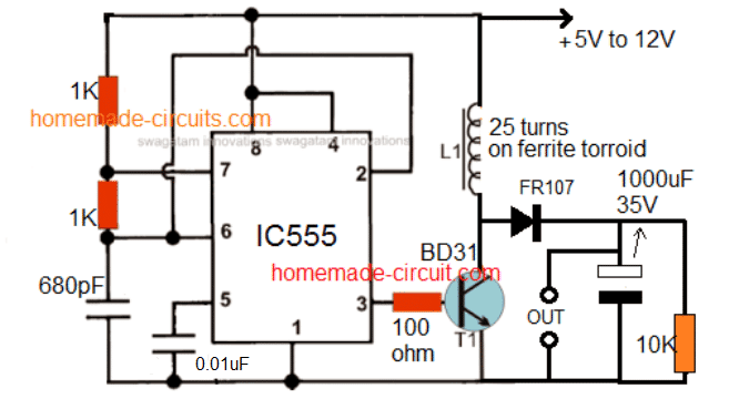
This simple circuit is built using an IC 555 circuit for boosting USB 5V to 24V, or any other desired level. The same design can be used for boosting a 3.7 V to 24 V from a Li-Ion cell.
Let's assume we have the following parameters required for the above circuit:
Important Parameters:
- Input Voltage (Vin): 5V
- Output Voltage (Vout): 24V
- Output Current (Iout): 1A
- Switching Frequency (f): 50 kHz
Calculating the Part Values
Step 1: Output Power
Pout = Vout * Iout = 24V * 1A = 24WEfficiency (η) = 85%
Pin = Pout / η = 24 / 0.85 ≈ 28.2WInput Current (Iin) = Pin / Vin = 28.2 / 5 ≈ 5.64AStep 2: Inductor Selection
Inductance (L) = (Vin * D) / (f * ΔI)D = 1 - (Vin / Vout) = 1 - (5 / 24) ≈ 0.79Ripple Current (ΔI) = 0.4 * Iin = 0.4 * 5.64 ≈ 2.26AL = (5 * 0.79) / (50000 * 2.26) ≈ 35µHChoose an inductor with L = 35µH, capable of handling at least 6A peak current.
Step 3: Diode Selection
Reverse Voltage: ≥ Vout = 24VForward Current: ≥ Iout = 1AChoose a Schottky diode, such as MBR360 (60V, 3A).
Step 4: Capacitor Selection
Output Capacitor (C) = (Iout * D) / (f * ΔV)Assume Ripple Voltage (ΔV) = 1V:
C = (1 * 0.79) / (50000 * 1) ≈ 16µFChoose a low-ESR electrolytic capacitor, such as 100µF, 35V.
Step 5: Resistor Selection for 555 Timer
Frequency (f) = 1.44 / ((R1 + 2R2) * C1)Assume C1 = 0.01µF:
R1 + 2R2 = 1.44 / (50 * 103 * 0.01 * 10-6) = 2.88kΩSet R1 = 1kΩ, then 2R2 = 1.88kΩ, so R2 = 940Ω.
Use standard values: R1 = 1kΩ, R2 = 1kΩ.
Finalized Part values for the above 555 boost Converter Circuit
L1: 35µH, 6A
D1: MBR360 (60V, 3A Schottky)
Cout: 100µF, 35V (low ESR)
R1 & R2: 1kΩ each
C1 (timing): 0.01µF
T1 (switch): BD31 or better NPN transistor capable of 6A or a MOSFET (e.g., IRF540N)
Construction Steps (How to Assemble)
Step 1: Build the Oscillator Circuit
Assemble the 555 timer circuit on a breadboard or PCB.
Use the formula for the 555 timer frequency:
f = 1.44 / ((R1 + 2R2) * C1)Select the appropriate values for R1, R2, and C1 to achieve the desired switching frequency (e.g50 kHz).
Connect the output of the 555 timer (pin 3) to the base or the gate of the switching transistor/MOSFET through the resistor (e.g 100Ω).
Step 2: Connect the Inductor and Switching Transistor
Solder the inductor (e.g.35µH) in series with the input voltage and the collector (or drain) of the switching transistor.
Connect the emitter (or source) of the transistor to ground.
Step 3: Add the Diode
Solder the Schottky diode (e.g MBR360) between the inductor and the output capacitor.
Connect the cathode of the diode to the positive terminal of the output capacitor.
Step 4: Connect the Output Capacitor
Add an electrolytic capacitor (e.g., 100µF 35V) across the output terminals for to smooth out the boosted DC voltage.
Step 5: Feedback/Control (Optional)
For adjustable output voltage you can include a feedback circuit with a variable resistor (potentiometer) to adjust the duty cycle of the PWM signal.
Step 6: Add Input and Output Terminals
Solder the connectors or terminals for the input voltage (Vin) and output voltage (Vout).
Step 7: Verify Connections
Double-check all the connections to ensure that there are no shorts or loose connections.
Testing the Circuit
Connect the 5V DC power supply to the input terminals.
Measure the output voltage using the multimeter to ensure that it reaches the desired value (e.g.,, 24V).
Adjust the duty cycle (if applicable,) to fine-tune the output voltage.
Connect the load (e.g, a resistor or a small motor) to the output and measure the current.
Assembly Tips
Use the heat sink for the transistor or MOSFET to dissipate the heat during the operation.
Keep the connections between the inductor, switch, diode, and the capacitor as short as possible to minimize the losses.
Use the printed circuit board (PCB) for getting a robust and reliable assembly.
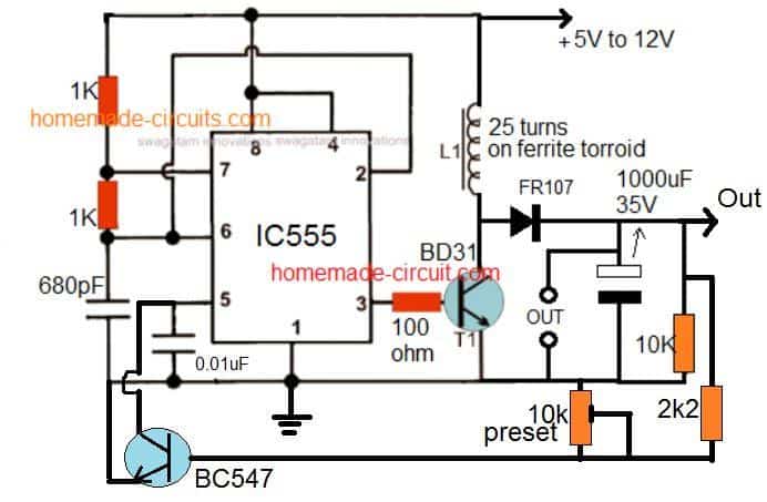
Adding a Feedback
The above circuit can be regulated with a feedback as shown below:
The idea looks quite straightforward. IC 555 is configured as an astable multivibrator whose frequency is decided by the values of resistors and capacitor at pin#7 and pin#6/2.
This frequency is applied to the base of a driver transistor TIP31 (incorrectly shown as BD31).
The transistor oscillates at the same frequency and forces supply current to oscillate within the connected inductor with the same frequency.
The selected frequency saturates the coil and boosts the voltage across it to a greater amplitude which is measured to be around 24V.
This value can be tweaked to even higher levels by modifying the turns of the inductor and the frequency of the IC .
Video Demonstration for IC 555 Boost Converter circuit
How a Boost Converter Works (Theoretical Analysis)
A boost converter is a kind of SMPS or switch mode power supply which fundamentally works with two active semiconductors (transistor and diode) and with a minimum of one passive component in the form of a capacitor or an inductor or both for greater efficiency.
The inductor here basically is used for stepping up the voltage and the capacitor is introduced for filtering the switching fluctuations and for reducing current ripples at the output of the converter.
The input power supply which may be required to be boosted or stepped up could be acquired from any suitable DC source such as batteries, solar panels, motor based generators etc.
Operating Principle
The inductor in a boost converter plays the important of stepping up the input voltage.
The crucial aspect which becomes responsible for activating the boost voltage from an inductor is due to its inherent property of resisting or opposing a suddenly induced current across it, and due to its response to this with a creation of magnetic field and subsequently destroying of the magnetic field. The destroying leads to the releasing of the stored energy.
This above process results in the storing of the current in the inductor and kicking back this stored current across the output in the form of back EMF.
A relay transistor driver circuit can be considered a great example of a boost converter circuit. The flyback diode connected across the relay is introduced to short circuit the reverse back EMFs from the relay coil and to protect the transistor whenever it switches OFF.
If this diode is removed and a diode capacitor rectifier is connected across the transistor's collector/emitter, the boosted voltage from the relay coil can be collected across this capacitor.
The process in a boost converter design results in an output voltage that’s always higher than the input voltage.
Boost Converter Configuration
Referring to the following figure, we can see a standard boost converter configuration, the working pattern may be understood as given under:
When the shown device (which could be any standard power BJT or a mosfet) is switched ON, current from the input supply enters the inductor and flows clockwise through the transistor to complete the cycle at the negative end of the input supply.

During the above process the inductor experiences a sudden introduction of current across itself and tries to resist the influx, which results in the storing of some amount of the current in it through the generation of a magnetic field.
At the next subsequent sequence, when the transistor is switched OFF, the conduction of current breaks, yet again forcing a sudden change in the current level across the inductor.
The inductor responds to this by kicking back or releasing the stored current. Since the transistor is in the OFF position, this energy finds its path through the diode D and across the shown output terminals in the form of a back EMF voltage.

The inductor performs this by destroying the magnetic field which was earlier created in it while the transistor was in the switch ON mode.
However, the above process of releasing energy is implemented with an opposite polarity, such that the input supply voltage now becomes in series with the inductor back emf voltage. And as we all know that when supply sources join in series their net voltage adds up to produce a bigger combined outcome.
The same happens in a boost converter during the inductor discharge mode, producing an output which may be the combined result of the inductor back EMF voltage and the existing supply voltage, as shown the diagram above
This combined voltage results in a boosted output or a stepped up output which finds its path through the diode D and the across capacitor C to ultimately reach the connected load.
The capacitor C plays quite an important role here, during the inductor discharge mode the capacitor C stores the released combined energy in it, and during the next phase when the transistor switches OFF again and the inductor is in the storing mode, the capacitor C tries to maintain the equilibrium by supplying its own stored energy to the load. See the figure below.

This ensures a relatively steady voltage for the connected load which is able to acquire power during both the ON, and OFF periods of the transistor.
If C is not included then this feature is cancelled resulting in a lower power for the load and lower efficiency rate.
The above explained process continues as the transistor is switched ON/OFF at a given frequency, sustaining the boost conversion effect.
Modes of Operation
A boost converter may be primarily operated in two modes: the continuous mode, and the discontinuous mode.
In continuous mode, the inductor current is never allowed to reach zero during its discharging process (while the transistor is switched OFF).
This happens when the ON/OFF time of the transistor is dimensioned in such a way that the inductor is always connected back quickly with the input supply through the switched ON transistor, before it’s able to get completely discharged across the load and the capacitor C.
This allows the inductor to consistently produce the boost voltage at an efficient rate.
In the discontinuous mode, the transistor switch ON timing may be so wide apart that the inductor may be allowed to get discharged fully and stay inactive in between the switch ON periods of the transistor, creating huge ripple voltages across the load and the capacitor C.
This could make the output less efficient and with more fluctuations.
The best approach is to calculate the ON/OFF time of the transistor which yields maximum stable voltage across the output, meaning we need to make sure that the inductor is optimally switched such that it’s neither switched ON too quickly which might not allow it to discharge optimally, and nor switch it ON very late which might drain it an inefficient point.
Calculating, Inductance, Current, Voltage and Duty Cycle in a Boost Converter
Here we’ll discuss only the continuous mode, which is the preferable way to operate a boost converter. Let’s evaluate the calculations involved with a boost converter in continuous mode:
Inductor Current Build-Up (Transistor ON Phase)
While the transistor is in the switched ON phase, the input source voltage (Vi) is applied across the inductor, inducing a current (IL) build-up through the inductor for a time period (t). This can be expressed as:
dIL/dt = Vi/LBy the time the ON state of the transistor ends and it switches OFF, the current built up in the inductor can be calculated using:
ΔIL(on) = Vi × D × T / LWhere:
- D is the duty cycle.
- L is the inductance value of the inductor (Henry).
- T is the switching period.
Inductor Discharge (Transistor OFF Phase)
When the transistor is OFF, assuming the diode offers minimal voltage drop and the capacitor (C) is large enough to maintain a constant output voltage, the output current (IL) can be deduced as:
Vi - Vo = L × dIL/dtThe current variation (ΔIL) across the inductor during the discharge phase can be expressed as:
ΔIL(off) = (Vi - Vo) × (1 - D) × T / LSteady-State Operation
Under steady conditions, the energy stored in the inductor during the ON phase equals the energy released during the OFF phase. This implies:
ΔIL(on) + ΔIL(off) = 0Substituting the expressions for ΔIL(on) and ΔIL(off):
Vi × D × T / L - (Vi - Vo) × (1 - D) × T / L = 0Simplifying:
Vo / Vi = 1 / (1 - D)Or equivalently:
Vo = Vi / (1 - D)This shows that the output voltage in a boost converter is always higher than the input voltage across the full range of duty cycles (0 < D < 1).
The duty cycle can be calculated as:
D = 1 - Vi / VoPower Stage Calculation
To calculate the boost converter’s power stage, the following guidelines are necessary:
- Input Voltage Range: Vin(min) and Vin(max)
- Minimum Output Voltage: Vout
- Maximum Output Current: Iout(max)
- IC specifications: Choose based on the IC’s datasheet.
Determining Maximum Switching Current
The first step is to calculate the duty cycle at the minimum input voltage:
D = 1 - (Vin(min) × η) / VoutWhere:
- Vin(min) = minimum input voltage
- Vout = output voltage
- η = efficiency (e.g., 80%)
Calculating Ripple Current
The ripple current can be calculated as:
ΔIL = Vin(min) × D / (f × L)Where:
- f = minimum switching frequency
- L = inductor value
Maximum Output Current Check
Verify the IC’s maximum output current:
Iout(max) = [Ilim(min) - ΔIL / 2] × (1 - D)Where:
- Ilim(min) = minimum current limit from the IC datasheet
- ΔIL = ripple current
If the calculated Iout(max) is insufficient, choose a new IC with a higher current limit or increase the inductor value to reduce ΔIL.
Maximum Switch Current
The maximum switch current can be calculated as:
Isw(max) = ΔIL / 2 + Iout(max) / (1 - D)Inductor Selection
For inductors:
L = Vin × (Vout - Vin) / (ΔIL × f × Vout)Choose an inductor with a current rating higher than Isw(max).
Inductor Ripple Current Approximation
Approximate the ripple current as 20% to 40% of Iout(max):
ΔIL = (0.2 to 0.4) × Iout(max) × Vout / VinRectifier Diode Selection
For the rectifier diode, use:
If = Iout(max)The diode’s power dissipation can be calculated as:
Pd = If × VfWhere:
- If = average forward current of the diode
- Vf = forward voltage of the diode
Schottky diodes are recommended due to their low forward voltage drop and high peak current rating.
Output Voltage Setting
Most converters set the output voltage using a resistive divider network (this may be built-in for fixed output voltage converters).
With the given feedback voltage Vf and feedback bias current Ifb, the voltage divider can be calculated. The current through the resistive divider should ideally be about 100 times the feedback bias current:
Ir1_2 >= 100 * Ifb ---------- (9)Where:
- Ir1_2 is the current through the resistive divider to GND.
- Ifb is the feedback bias current from the datasheet.
This ensures less than 1% inaccuracy in the voltage measurement. However, lower resistor values can increase power loss in the resistive divider, which may be unsuitable for high-efficiency designs.
With the above condition, the resistors can be calculated as follows:
R2 = Vf / Ir1_2  ---------- (10)

R1 = R2 * [(Vout / Vf) - 1]  ---------- (11)
Where:
- R1 and R2 are the resistive divider resistors.
- Vf is the feedback voltage from the datasheet.
- Ir1_2 is the current through the resistive divider to GND, as calculated in Equation 9.
- Vout is the desired output voltage.
Input Capacitor Selection
The minimum value for the input capacitor is typically specified in the datasheet. This value is crucial for stabilizing the input voltage under the peak current requirements of a switching power supply.
Low ESR ceramic capacitors are preferred, and the dielectric material should be X5R or better. This avoids significant capacitance reduction due to DC bias or temperature effects.
If the input voltage is noisy, the capacitance value may need to be increased.
Output Capacitor Selection
To reduce output voltage ripple, small ESR capacitors are ideal. Ceramic capacitors with an X5R dielectric or better are recommended.
For converters with external compensation, any capacitor value above the minimum specified in the datasheet can be used.
However, the compensation must be adjusted accordingly. For internally compensated converters, the recommended inductor and capacitor values should be followed, or the datasheet guidelines should be used.
For secondary compensation, the following equations can help adjust output capacitor values for a desired output voltage ripple:
Cout_min = Iout_max * D / (fs * ΔVout) ---------- (12)Where:
- Cout_min is the minimum output capacitance.
- Iout_max is the maximum output current of the application.
- D is the duty cycle calculated using Equation 1.
- fs is the minimum switching frequency of the converter.
- ΔVout is the desired output voltage ripple.
The ESR of the output capacitor introduces additional ripple, calculated as:
ΔVout_ESR = ESR * [(Iout_max / (1 - D)) + (ΔIL / 2)] ---------- (13)Where:
- ΔVout_ESR is the additional output voltage ripple caused by the capacitor's ESR.
- ESR is the equivalent series resistance of the output capacitor.
- Iout_max is the maximum output current of the application.
- D is the duty cycle from Equation 1.
- ΔIL is the inductor ripple current from Equation 2 or Equation 6.
Important Equations for Boost Converter Power Stage
Maximum Duty Cycle:
D = 1 - (Vin_min * n / Vout) ---------- (14)Where:
- Vin_min is the minimum input voltage.
- Vout is the desired output voltage.
- n is the efficiency of the converter (e.g., 85%).
Inductor Ripple Current:
ΔIL = Vin_min * D / (fs * L) ---------- (15)Where:
- Vin_min is the minimum input voltage.
- D is the duty cycle from Equation 14.
- fs is the nominal switching frequency of the converter.
- L is the chosen inductor value.
Maximum Output Current of the Selected IC:
Iout_max = [Ilim_min - ΔIL] * (1 - D) ---------- (16)Where:
- Ilim_min is the minimum current limit of the integrated switch (from the datasheet).
- ΔIL is the inductor ripple current from Equation 15.
- D is the duty cycle from Equation 14.
Application-Specific Maximum Switch Current:
Isw_max = (ΔIL / 2) + (Iout_max / (1 - D)) ---------- (17)Where:
- ΔIL is the inductor ripple current from Equation 15.
- Iout_max is the maximum output current of the application.
- D is the duty cycle from Equation 14.
Inductor Calculation:
L = Vin * (Vout - Vin) / (ΔIL * fs * Vout) ---------- (18)Where:
- Vin is the nominal input voltage.
- Vout is the desired output voltage.
- fs is the minimum switching frequency of the converter.
- ΔIL is the estimated inductor ripple current (see Equation 19).
Inductor Ripple Current Estimation:
ΔIL = (0.2 to 0.4) * Iout_max * (Vout / Vin) ---------- (19)Where:
- ΔIL is the estimated inductor ripple current.
- Iout_max is the maximum output current required.
Rectifier Diode Parameters:
- Forward Current:
If = Iout_max ---------- (20)- Power Dissipation:
Pd = If * Vf ---------- (21)Where:
- If is the average forward current of the rectifier diode.
- Vf is the forward voltage of the rectifier diode.
Resistive Divider Network:
- Current:
Ir1_2 >= 100 * Ifb ---------- (22)- Resistor R2:
R2 = Vf / Ir1_2 ---------- (23)- Resistor R1:
R1 = R2 * [(Vout / Vf) - 1] ---------- (24)Output Capacitance:
Cout_min = Iout_max * D / (fs * ΔVout) ---------- (25)Ripple Due to ESR:
ΔVout_ESR = ESR * [(Iout_max / (1 - D)) + (ΔIL / 2)] ---------- (26)These equation provide a comprehensive guide for designing and analyzing the power stage of a boost converter.


Good morning Sir.
Thank you for the great work you are doing.
Sir, I need a DC to DC converter circuit diagram to use in a mobile PA System that can deliver up to 100Watt or more from a 12V DC lithium battery
Thank you so much Ngang, is it a boost converter or a buck converter, please provide the full specifications of the converter, I will try to figure it out….
Dear Sir, I have a situation where the input supply voltage is one volt.
This is the ONLY voltage available, so obviously a 555 cannot be used for the square wave signal to the transistor base.
What simple remedy is there for this.
I need about up to 8 volts output.
There is plenty of amperage available at the one volt input supply.
Thanks,
Steele Braden.
Hello Steele, You can try a joule thief circuit concept, as explained in the following article:
https://www.homemade-circuits.com/1-watt-led-driver-using-joule-thief/
https://www.homemade-circuits.com/8x-overunity-circuit-using-joule-thief/
I am trying to make 2 similar circuits that can take 2 AA batteries and output 9, and 18V DC, would this process work for making those circuits or do you have other suggestions.
1 circuit needs to take 3V in and output 18V DC, the other needs to output 9V DC
For your application a joule thief circuit might be more suitable:
https://www.homemade-circuits.com/1-watt-led-driver-using-joule-thief/
Hello sir, hope you’re doing well
Pls how can I trigger a MOSFET IRFZ44N with BJT since my pulse voltage is 5v and the vgs(gate voltage of the MOSFET is 10v)to trigger it appropriately ?
Hello Akafac,
If you are having a separate 10V DC then you will need two BC547 to amplify and invert the 5V to 10V.
If you do not have a separate 10V then you may need a boost converter circuit.
https://www.homemade-circuits.com/wp-content/uploads/2023/04/1.5V-to-3.3V-boost-converter-circuit-for-LEDs.jpg
Greatings sir pls on your 1st diagram simple smps boost converter I tried to run the simulation but my proteous display 2 error sms
1 was stating no specification for D1 (FR107)
2nd pls is the zener operating ?
Hi Akafac,
It is difficult to tell why the simulation is showing the error.
You can try the following design instead and let me know how it goes:
https://www.homemade-circuits.com/wp-content/uploads/2018/05/joule-thief-1.jpg
Pls sir for the above circuit I’ll need the specifications of TR1 on the diagram
For the exact specifications you can refer to the following diagram:
https://www.homemade-circuits.com/wp-content/uploads/2024/02/simple-joule-thief-circuit.jpg
For the transistor, please use a TIP122, for handling 1 amp current.
Thanks very much sir pls I have seen and article online on this topic I want to share with you but your email isn’t reachable I have simulated it it’s almost on point but pls I need some guidance sir
Pls can you send me your email to my Gmail so that I forward to you the link to it sir ? Thanks
Akafac, unfortunately I do not work with simulators, instead I use my knowledge based brain simulation and finally by testing through practical experimentation. I have tested the above circuit and it works wonderfully well.
If you any other questions regarding the circuit working, please let me know, i will try to help.
Greatings sir, pls my 5v to 12v boost converter I couldn’t calculate the inductor value and filtering capacitor value that will give me a constant 12v out I intend to take in 5v , send out 12v , out put current of 2A taking in to consideration a feedback system but my switch should be trigger by a pulse sign maybe generated by NE555 which is supply by a 5v dc in put which oscillate to generate the pwm to drive my switching regulator
Pls sir I need your total help again
My specifications are
1 input 5v , output 12v , output current 2A,
Thank
Hello Akafac, here are the calculations for your application:
Specifications:
Input Voltage = 5V
Output Voltage = 12V
Load Current = 2 Amps
Duty Cycle Calculation:
D = 1 – (Vin / Vout)
D = 1 – (5 / 12)
D = 0.5833 (58.33%)
Output Power:
Pout = Vout * Iout
= 12 * 2
Pout = 24W
Input Current:
Assume efficiency (η) = 80% = 0.8
Iin = Pout / (Vin * η)
= 24 / (5 * 0.8)
= 24 / 4
Iin = 6A
Inductor Value:
L = (Vin * D) / (f * ΔIL)
Where ΔIL = Ripple Current = 20% of Iin = 0.2 * 6 = 1.2A
Assume switching frequency (f) = 50kHz = 50,000 Hz
L = (5 * 0.5833) / (50,000 * 1.2)
L = 2.9167 / 60,000
L = 48.61 µH
Choose standard value: 47 µH
Output Capacitor Value:
Cout = (Iout * D) / (f * ΔVout)
Where ΔVout = Output Ripple Voltage = 0.1V
Cout = (2 * 0.5833) / (50,000 * 0.1)
Cout = 1.1667 / 5,000
Cout = 233.33 µF
Choose standard value: 220 µF or use parallel capacitors.
Resistor Values for IC 555:
Frequency formula: f = 1.44 / ((R1 + 2R2) * Ct)
Assume Ct = 10 nF = 0.00000001 F
R1 + 2R2 = 1.44 / (f * Ct)
R1 + 2R2 = 1.44 / (50,000 * 0.00000001)
R1 + 2R2 = 1.44 / 0.0005
R1 + 2R2 = 2880 Ω
Choose R1 = 1 kΩ = 1000 Ω
2R2 = 2880 – 1000
2R2 = 1880 Ω
R2 = 1880 / 2
R2 = 940 Ω
Sir, thank very much God blessed you for your good works indeed I acknowledge your kind heart
You are most welcome Akafac.
Greatings sir pls when calculating the capacitor value why did you assume ripple voltage of 1v, and for the inductor you assume o.4
Hello Akafac,
we must assume Ripple Current as a Percentage of Load Current if Input Current is Not Clearly specified.
If input current Iin cannot be estimated and an “optimal” ripple current is assumed, use a rule-of-thumb based on the load current (Iout):
Typical Design: Assume Δ I = 20-30% of Iout.
High-Efficiency Design: Assume Δ I = 10-15% of Iout.
Example:
For Iout = 2A:
Δ I = 0.2 * 2 = 0.4A (20%).
Δ I = 0.1 * 2 = 0.2A (10%)
Fine boosted sir but the out put voltage is not stable it’s increasing from 12v to 15v
Akafac, did you build it practically, or doing a simulation? because I cannot help with simulations, I can only help with practical working.
Try increasing the output capacitor value and check again.
Thanks very much sir, the PWM oscillator circuit with NE555 is working ok for 50khz, 58.33%
Pls I wish to add a feedback circuit to it pls how do I go about it?
Thanks Akafac, the feedback circuit is given at the end of the post.
Good day sir hope you’re doing well, pls my teacher ask me to used ATMEGA 32 to generate to PWM
Instead of NE555 pls help sir
Thanks
Sorry Akafac, my microcontroller programming knowledge is not good, so I may not be able to help you in this regard….
Thank you sir I applaud
You’re a kind person
Thank you Akafac, for your kind words, I appreciate it. I Hope you find someone who can do it for you…
Yes sir it’s working well but the diagram you gave me and the calculations are perfect I’m fine now my circuit is ok thanks sir
Thanks Akafac, Glad to know it is working. All the Best to you…
Hello sir, please I saw a 12v , 8A to 24v, 8A converter,
1. is this boost or buck converter because it increases the power?
2. please help Me with a circuit for it?
3. please how can I use such converter for infinity power supply?
Hi Daniel,
That is a boost converter, but the output current will not be 8 amps, it will be around 3.5 amps.
Power can never be boosted, output power will be always lower than the input power.
Thanks sir, engineer Swagatam, you are correct, it was typo error on the converter presentation.
No problem Daniel, glad it helped!
I have tried but very tedious by trial and error. Thanks for always.