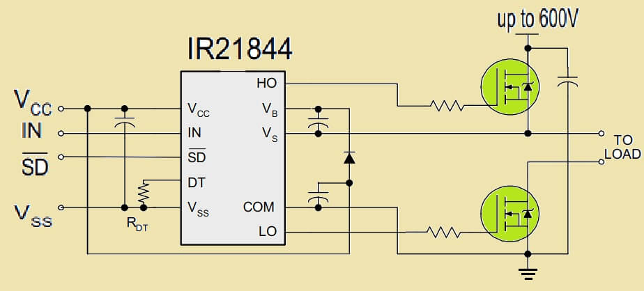
Many folks, especially beginners, they get fully confused when they try to use a half-bridge driver circuits using ICs like IR2184 or IR2110. They look at the datasheet diagram and start thinking, “Bro, how the load will conduct? The MOSFETs are switching one by one so how the current will pass through the load? Looks like the circuit is incomplete…”
But actually the datasheet is not wrong — it is just not fully showing the load connection in clear way. So here in this article we will try to fully break this thing down and explain — how exactly the load gets power and how it conducts in a half-bridge circuit.
First Let us Understand the Basic Half-Bridge MOSFET Section
We take two N-channel MOSFETs, and connect them like this:
- Top MOSFET (called high-side) has:
- Drain = connected to high voltage DC bus (like 310V or 600V DC)
- Source = connected to VS node (midpoint node)
- Bottom MOSFET (called low-side) has:
- Drain = connected to same VS node
- Source = connected to GND
So basically both MOSFETs are connected in series, and the middle point between them is called VS. This VS point is super important — this is where we take output to the load.
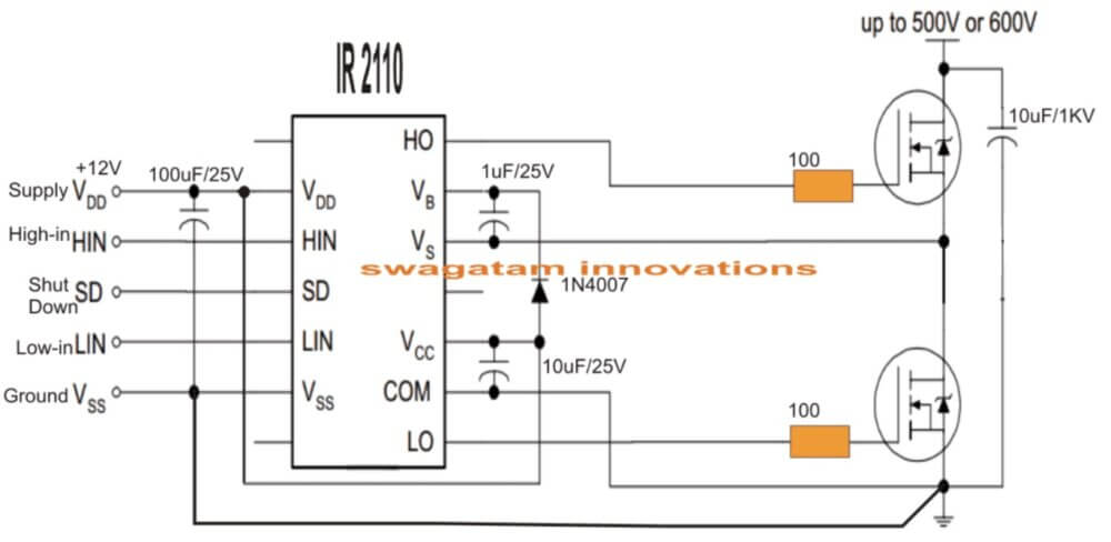
Then Comes the Confusion from Datasheet Diagram
Now if we see the official diagram from IR2184 or IR2110 datasheet, we will find that the “TO LOAD” point is connected to the VS node, which is correct.
But then it shows another “TO LOAD” terminal coming out from somewhere around low-side FET. But the datasheet does not show where this second terminal is going. That is what creates full confusion.
People start thinking:
“Bro, shall we connect the load between VS and drain of low-side FET? Then when high side is ON and low side is OFF, how will current complete the path?”
Yes that question is valid. And if we do not know how the circuit is meant to be wired in real life, we will get confused.
Correct Way to Connect Load in Half-Bridge
The real, proper way to connect the load (like a bulb or motor) is this:
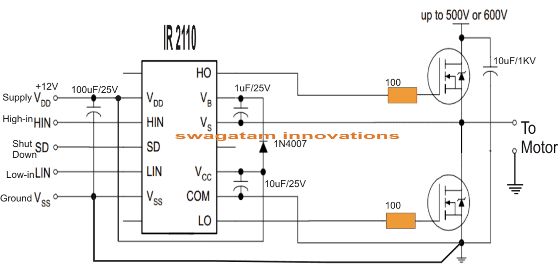
- One terminal of the load goes to the VS node which is the middle point between both MOSFETs.
- The other terminal of the load must go to system GND.
That is all. This is the correct method.
Load must be between VS and GND
Do not connect the load between VS and drain of low-side FET, that will never work properly.
So How Does the Load Conduct?
Now let us see what happens when the MOSFETs switch one by one.
When High-Side MOSFET is ON:
- Current flows like this:
+Vbus → High-side FET → VS node → Load → GND - So full supply voltage comes across load
- Load conducts, bulb glows
When Low-Side MOSFET is ON:
- VS node is now pulled to ground.
- Load sees 0V across it (both ends at GND).
- No current flows.
- Load stays OFF.
When you do PWM on high-side:
- Load gets pulsed voltage at PWM frequency.
- Load operates with average power based on duty cycle
- Motor can be speed controlled etc.
This is how half-bridge actually works.
If You Connect Load Wrongly
Suppose you make the mistake of connecting one terminal of the load to junction of High side MOSFET Source and the VS, and the other terminal of the load to drain of low-side FET. Then:
- When High-side MOSFET is ON then Load gets the full DC supply which is floating on its one terminal, but the load cannot operate because the low-side MOSFET is OFF, so circuit cannot complete.
- When low-side FET turns ON, the High-side MOSFET turns OFF, and then the other terminal of the load is pulled to ground, again the load cannot operate because the DC supply is not there (high-side turned OFF)
- That means when the MOSFETs switch alternately, both terminals of load are floating or shorted — so no real voltage appears across load
- Load does not get proper conduction path.
- Sometimes it may even damage FET or cause weird results.
So this load configuration is wrong and should never be used.
So, in our recommended, correct configuration the load (like a bulb or motor) is just sitting between the junction of High-side MOSFET source and VS, and the supply DC GND.
Whenever the high-side FET turns ON, the High-side MOSFET Source and VS junction becomes high (like 310V), and so the load gets voltage across it, so it gets powered and operates.
When high-side MOSFET is OFF and low-side is ON, then VS becomes 0V, so both ends of load now get 0V, so no conduction happens, load remains turned OFF.
This simple logic gives you pulsed DC to the load, controlled by your gate PWM.
Final Conclusion
- The datasheet diagram is not wrong — but it is incomplete. It does not show where the second load wire goes.
- You must manually connect the second load wire to GND.
- Load must always be between VS node and ground.
- Do not connect load between VS and any other random drain or point — it will not work.
- This is how half-bridge drivers like IR2184 or IR2110 properly operate the load.
So guys, next time when you use a half-bridge MOSFET driver, just remember this:
“Load must be connected between the junction of High-side MOSFET + VS and DC GND — that is all. High-side MOSFET ON means load gets full DC supply, low-side MOSFET ON means load goes OFF.”


Need Help? Please Leave a Comment! We value your input—Kindly keep it relevant to the above topic!