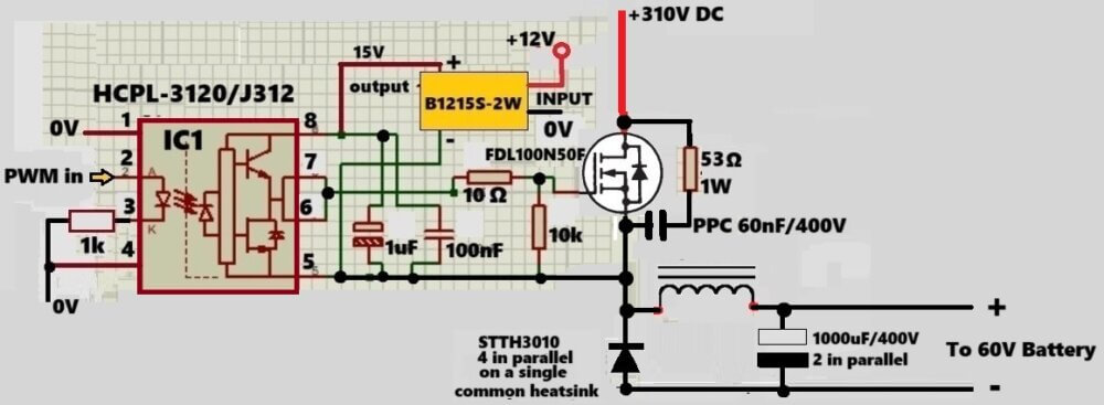
This is a high voltage 310V to 60V buck converter, so we have that big 310V DC coming in which we usually get after rectifying 220V AC mains. So now that high DC is there and we want to push it down to something like 60V or lower for battery charging or similar work.
Audio/Video Representation
Basic Working
We use a MOSFET here, that FDL100N50F, which is acting like a fast switch, not linear, just ON OFF kind of thing and an external PWM is controlling it.
So when MOSFET turns ON then current flows from that 310V line through MOSFET into the inductor, and the inductor stores energy at that time, like holding it for a moment.
When MOSFET turns OFF then inductor does not like current dropping suddenly. so it pushes that stored energy forward through the diode into the load, so now energy keeps moving even when switch is OFF, yep that is the main buck action.
So this ON OFF keeps repeating and because of that, output becomes lower DC, not 310V anymore.
Circuit Diagram
Output Voltage Depends on Input PWM Duty Cycle
Now output voltage depends on duty cycle, so more ON time means more output, less ON time means lower output, simple relation is there:
Vout = D × Vin
Where D is duty cycle and Vin is input.
Inductor and capacitor are chosen using formulas, like:
L = (Vin − Vout) × D / (f × ΔI)
and capacitor:
C = ΔI / (8 × f × ΔV)
What is ΔI
Here, ΔI, is the inductor ripple current.
In a buck converter, current is not straight DC, it becomes like a triangle shape, rising then falling, again rising, so now ΔI is just that full swing, top to bottom.
Means how much current goes up and comes down in one switching cycle, that full gap, that is ΔI.
If current goes from 2 A and then climbs to 2.4 A, then comes back, so now that difference is 0.4 A, so that is ΔI.
If ΔI is small, then current looks smoother, less stress on parts, but then inductor must be bigger, which is not always nice.
But if ΔI is large, then inductor can be smaller, however ripple increases, noise also comes in, so trade-off is there, you choose what fits.
What is ΔV
ΔV means output voltage ripple, simple, it is how much the voltage goes up and down, not steady, because switching is happening, so now even if capacitor is there, still it does not become perfect DC, some shake is always there.
See example, if voltage goes from 12.00 V to 12.05 V, then ΔV becomes 0.05 V, that is 50 mV ripple, small but still there, not flat.
Now design side, if ΔV is small then output looks clean, but then capacitor must be bigger, more work for it.
But if ΔV is big then capacitor can be small, however output becomes noisy, so tradeoff is there, you pick one side.
Now look at formulas, inductor one:
L = (Vin − Vout) × D / (f × ΔI)
Here ΔI sits below, so if ΔI becomes small then L must grow bigger, which makes sense, since smoother current needs bigger inductor..
Capacitor side:
C = ΔI / (8 × f × ΔV)
Now ΔV is below, so if ΔV becomes small then C must increase because better filtering is needed, so capacitor size goes up.
Designers usually do one thing, they do not go extreme, they pick middle range, so ΔI is kept around 20% to 40% of output current, and ΔV around 1% to 2% of output voltage, that gives decent balance, not too big parts, not too noisy.
Simple way to remember, ΔI tells how bumpy current is, ΔV tells how bumpy voltage is, L smooths current, C smooths voltage, that is it.
Using Isolated Gate Driver HCPL-3120 for the Input PWM
Now gate driving is not direct, we use that HCPL-3120, which is optocoupler type driver, so control side stays a bit safer from that high voltage side, not fully isolated system but still some separation is there.
For powering that driver, B1215S-2W is used which gives floating 15V, so even when MOSFET source moves up and down, driver still works properly, so now gate gets correct drive.
But see, input and output grounds are still common, so this is not full isolation, just partial safety.
Using Snubber for MOSFET Protection
There is also snubber, resistor and capacitor across MOSFET, which helps when spikes come, because switching creates sudden voltage jumps, so this network calms it down a bit and saves MOSFET stress.
Output side Components
Output side has fast diode, like STTH3010, sometimes many in parallel, then inductor and big capacitors, so that output becomes smooth DC, not noisy pulses.
Important Notes
Now practical things, heatsink is must, MOSFET and diodes both will heat, so without heatsink then things go bad quickly.
PCB layout also matters, if tracks are long or messy then noise and spikes increase so keep it tight.
If current goes too high then without control it can damage things, so current limiting is better to add.
Also feedback control, if not used then voltage can drift so better to monitor and regulate.
For PWM Control, we can use IC 555
Now for PWM we can use IC 555, simple and easy, as shown in the above image.
555 runs in astable mode, gives PWM, and duty cycle can be adjusted using resistor and diode trick.
Frequency is:
f = 1.44 / ((R1 + 2 × R2) × C)
Duty is:
D = (R1 + R2) / (R1 + 2 × R2)
If we separate charge and discharge using diode, then:
Ton = 0.693 × Rcharge × C
Toff = 0.693 × Rdischarge × C
D = Ton / (Ton + Toff)
Pin 3 gives output, that goes into optocoupler through resistor and potentiometer adjusts duty, so now output voltage of buck also changes.
Applications are many, like high voltage DC stepping down, battery charging, solar systems, industrial supplies, motor control, inverter front side.
Conclusion
So overall this circuit takes 310V DC and drops it to lower voltage using switching without wasting power like linear regulator, but you must design properly, cooling, layout, control, otherwise it can misbehave, since high voltage can be difficult to control...

Need Help? Please Leave a Comment! We value your input—Kindly keep it relevant to the above topic!