In this article we are going to see a simple SMPS circuit diagram which is using UC3843 IC. This circuit can convert 85V AC to 285V AC input into stable 12V DC output. UC3843 is very popular current mode PWM controller IC used in many power supply circuits. Below we will discuss full working and component details of this circuit.
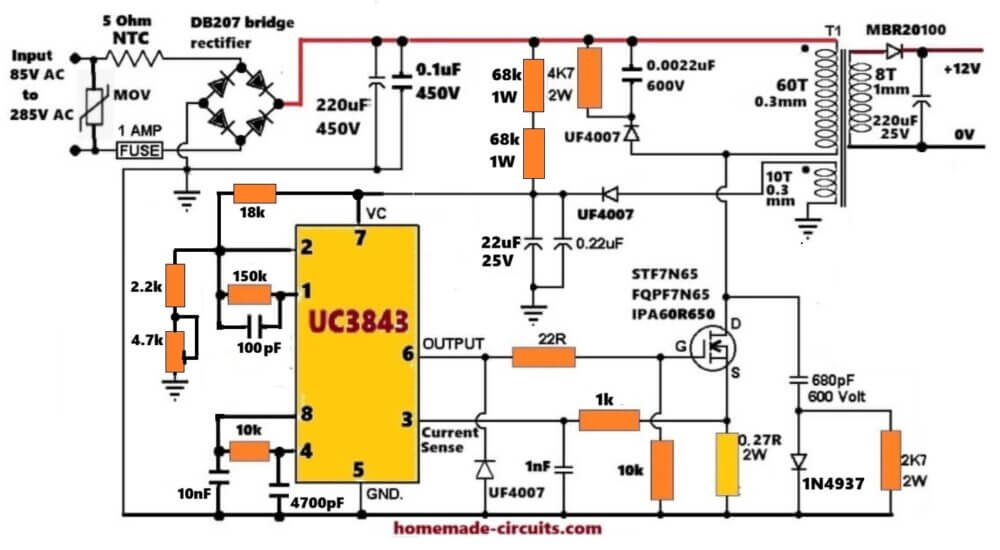
This UC3843 flyback SMPS circuit is designed for converting approximately 85V AC to 285V AC input into a regulated 12V DC output. The circuit uses primary side regulation through the auxiliary winding, so there is no optocoupler and no TL431 in this design.
The main idea of this circuit is simple. The 10-turn auxiliary winding produces a voltage which follows the main 12V output. This auxiliary voltage is rectified and used for two purposes. First, it powers pin 7 of the UC3843 after startup. Second, the same voltage is sensed through the 18k and 2.2k plus 4.7k adjustable resistor network and fed to pin 2. In this way, when the 12V output rises, the auxiliary voltage also rises, pin 2 voltage rises, and the UC3843 automatically reduces the PWM duty cycle.
The 18V external zener has now been removed. This is acceptable because the UC3843 itself includes an internal VCC clamp or zener action. According to the TI datasheet, the VCC clamp is around 34V typical, although the exact value and operating conditions must be considered. So the external 18V zener is not required for the normal feedback operation, because otherwise it can interfere with sensing the actual changing auxiliary voltage.
However, one very important thing must be understood here. The internal UC3843 VCC clamp is only an internal protection feature, it is not a precision 18V regulator. Therefore the feedback divider must regulate the auxiliary voltage well below the internal clamp level during normal operation. The internal clamp should normally remain inactive.
Previously I had included an 18V zener at pin#7 for extra protection to the pin#7 of the IC. But because feedback was also associated with this line, so I had to remove the 18V zener so that feedback could correctly sense the fluctuating auxiliary voltage and regulate the output 12V correctly.
So now because pin#7 has no 18V clamp zener diode, the 22uF capacitor at pin 7 should not be only 25V rated. I would strongly suggest using at least a 35V capacitor, and preferably 50V for better safety margin.
If there is any feedback failure or startup overshoot, the internal clamp voltage can be much higher than 25V. So this is one important correction for the revised circuit.
How the input section works
The 85V AC to 285V AC input is first applied through the 5 ohm NTC resistor and the input protection components. The bridge rectifier converts the AC into high voltage DC.
At 85V AC input, the rectified DC can be around 120V DC.
At 220V AC input, the rectified DC can be around 311V DC.
At 285V AC input, the rectified DC can reach around 403V DC.
The 220uF 450V capacitor filters this DC bus.
Since the maximum input is 285V AC, the DC bus can reach around 403V, so the 450V capacitor is operating with only around 47V margin. This can work, but the capacitor should be a good quality 450V type and suitable for high ripple current.
How the UC3843 starts
Initially the UC3843 is not running, so the auxiliary winding is not producing any voltage. The two 68k resistors connected in series slowly charge the 22uF VCC capacitor. The total resistance is 136k.
When pin 7 reaches the UC3843 startup threshold, which is around 8.4V typical for UC3843, the IC starts oscillating.
After oscillation begins, the 10-turn auxiliary winding starts producing voltage. This voltage is rectified through the UF4007 diode and now takes over the VCC supply of pin 7.
The two 68k startup resistors are then no longer required to provide the main operating current. They only provide the initial startup current.
The UC3843 has a typical turn-off threshold around 7.6V. Therefore, after startup, the auxiliary winding must keep pin 7 comfortably above this voltage. If the auxiliary voltage is too low, pin 7 will fall below the turn-off threshold, the IC will stop, and then the startup resistors will again charge the capacitor. This can create repeated start-stop operation.
Using 22uF instead of the previous 100uF capacitor is a better choice here because the startup resistors have limited current. The smaller 22uF capacitor allows pin 7 to reach the startup threshold faster.
I would also add a 100nF ceramic capacitor directly between pin 7 and pin 5, physically as close as possible to the UC3843. The TI datasheet also recommends close ceramic bypassing of the VCC pin.
How the auxiliary winding feedback works
The important feature of this design is that there is no optocoupler.
The 10-turn auxiliary winding is magnetically coupled with the 8-turn 12V secondary winding. Therefore, when the 12V output voltage rises, the auxiliary winding voltage also rises. When the 12V output falls, the auxiliary winding voltage also falls.
The auxiliary winding voltage is rectified by the UF4007 diode. This rectified voltage charges the 22uF capacitor and powers pin 7. The same VCC voltage is also fed through the 18k resistor to pin 2 of the UC3843. From pin 2 to ground, there is a 2.2k fixed resistor in series with the 4.7k adjustable resistor.
This resistor network divides the auxiliary voltage and sends a scaled voltage to pin 2. The UC3843 internal error amplifier compares pin 2 with its internal approximately 2.5V reference. So the operation is like this.
If the 12V output starts rising above the required level, the auxiliary voltage also rises.
The voltage at pin 2 rises. When pin 2 tends to rise above the internal 2.5V reference level, the error amplifier changes the COMP pin voltage. The PWM duty cycle is reduced.
MOSFET ON time reduces.
Less energy is transferred to the transformer. The 12V output falls back toward the required level.
When the 12V output falls too low, the auxiliary voltage also falls. Pin 2 voltage falls below the required feedback level. The UC3843 increases the PWM duty cycle.
MOSFET ON time increases.
More energy is transferred to the output. The 12V output rises again. This continuous action regulates the output.
Why the 4.7k resistor can be made variable
Yes, in this circuit the 4.7k resistor can be used as an adjustable resistor because it changes the feedback divider ratio. The 2.2k fixed resistor is useful because it prevents the lower feedback resistance from becoming zero.
So the lower feedback resistance is: 2.2k plus the adjustable value of the 4.7k preset. By adjusting this resistance, you can select the auxiliary winding voltage at which pin 2 reaches approximately 2.5V. This allows the circuit to be calibrated so that the main output becomes exactly 12V.
For example, if the lower resistance is increased, the pin 2 voltage rises for the same auxiliary voltage. Therefore the converter will regulate at a lower auxiliary voltage.
If the lower resistance is reduced, a higher auxiliary voltage is required before pin 2 reaches 2.5V. Therefore the converter regulates at a higher auxiliary voltage.
The 2.2k fixed resistor plus the 4.7k preset gives a reasonably wide adjustment range.
But the preset should be adjusted while monitoring the actual main output voltage. Do not adjust it only by calculating the auxiliary winding voltage because diode drops, winding resistance, load current and transformer coupling can change the actual relationship between the 12V output and the auxiliary voltage.
For best calibration, connect the intended load to the output, set the circuit at a normal mains voltage, and slowly adjust the preset until the output is exactly 12.00V.
Then check the output again at minimum input voltage, maximum input voltage, no load and full load.
This type of auxiliary winding feedback can regulate reasonably well, but it cannot normally be expected to have the same precision as direct secondary-side sensing using TL431 and optocoupler. If very tight regulation is required over the complete load range, optocoupler feedback is still the better method.
How the pin 1 compensation network works
Pin 1 is the COMP pin, which is the output of the internal error amplifier. The 150k resistor and 100pF capacitor form the compensation network. This network is much more suitable than the previous circuit where a large 100nF capacitor was directly connected at pin 1 along with other confusing resistor connections.
The 100pF capacitor mainly helps to reduce high frequency noise and the 150k resistor provides compensation control.
The exact values may require practical adjustment depending on the transformer, output capacitor and load characteristics, but this arrangement is much more reasonable as a basic compensation network.
The oscillator section
Pin 8 provides the regulated 5V reference. The 10k resistor connects from pin 8 to pin 4. The 10nF capacitor connects from pin 4 to ground. This is the UC3843 oscillator timing network.
The UC3843 datasheet gives the approximate oscillator formula as:
Frequency = 1.72 divided by RT multiplied by CT
With 10k and 10nF, the frequency is approximately 17.2kHz.
Since UC3843 output switching frequency is the same as the oscillator frequency, the MOSFET will switch at approximately 17.2kHz.
The 10k resistor should not be removed because it is required for charging the timing capacitor.
MOSFET gate drive section
Pin 6 of the UC3843 drives the MOSFET gate through the 22 ohm resistor. The 22 ohm resistor helps control the MOSFET gate charging current and reduces excessive ringing. The 10k resistor from gate to source keeps the MOSFET normally OFF when the UC3843 output is inactive or during startup.
The MOSFET can be ST7FN65, FQPF7N65 or another suitable high voltage MOSFET with sufficient voltage and current margin.
Since the maximum rectified input can reach approximately 403V DC, the MOSFET must withstand the DC bus plus the reflected flyback voltage and the leakage inductance spike.
Therefore a proper drain clamp or snubber is important.
Current limiting section
The MOSFET source current flows through the 0.27 ohm current sensing resistor. This produces a voltage proportional to the MOSFET current. The signal is fed to pin 3 through the 1k resistor. The 1nF capacitor helps filter the high frequency switching spike.
The UC3843 current sense comparator trips at approximately 1V.
Therefore the theoretical peak primary current is around 3.7A.
When the current reaches this level, the UC3843 terminates the PWM pulse.
This provides cycle-by-cycle current limiting.
Drain spike suppression section
The 680pF capacitor, 2.7k resistor and 1N4937 diode form the drain spike suppression network. These components should not be removed blindly. When the MOSFET switches OFF, transformer leakage inductance can produce a sharp voltage spike at the MOSFET drain.
Since this circuit can operate from up to approximately 403V DC input, the drain voltage stress can become very high. The snubber network helps absorb or control these spikes.
The exact component values may need to be changed after checking the MOSFET drain waveform with an oscilloscope, but some form of spike suppression is normally required.
Output section
The 8-turn secondary winding produces the required flyback voltage.
The MBR20100 Schottky diode rectifies the output. The 220uF output capacitor filters the DC and produces the 12V output. The transformer uses a 10-turn auxiliary winding for powering the UC3843 and providing the feedback signal.
Because the auxiliary winding has 10 turns while the main secondary has 8 turns, its voltage is expected to be higher than the 12V output. The exact auxiliary voltage cannot be assumed only from the turns ratio because the two output rectifier diode drops and winding losses are different. Therefore, the 4.7k feedback preset is useful for final calibration.
Calculations
Maximum rectified DC voltage at 285V AC:
285 x 1.414 = 403V DC approximately
Rectified DC voltage at 220V AC:
220 x 1.414 = 311V DC approximately
Rectified DC voltage at 85V AC:
85 x 1.414 = 120V DC approximately
Total startup resistance:
68k + 68k = 136k
Startup resistor current at 285V AC and approximately 8.4V VCC:
(403 - 8.4) divided by 136000 = approximately 2.9mA
Total startup resistor power near maximum input:
approximately 1.1W total
Power in each 68k resistor:
approximately 0.55W
Therefore each 68k 1W resistor is reasonably loaded.
Approximate oscillator frequency:
Frequency = 1.72 divided by RT x CT
Frequency = 1.72 divided by 10000 x 10nF
Frequency = approximately 17200Hz
So switching frequency is approximately 17.2kHz.
Current limit calculation:
Peak current = 1V divided by 0.27 ohm
Peak current = approximately 3.7A
Feedback voltage equation:
Pin 2 voltage = VCC x lower resistance divided by 18k plus lower resistance
The lower resistance is:
2.2k plus the adjusted value of the 4.7k preset
To make pin 2 equal approximately 2.5V, the required auxiliary voltage is:
VCC = 2.5 x 18k plus lower resistance, divided by lower resistance
If lower resistance is 2.2k only:
Required auxiliary voltage is approximately 23V
If total lower resistance is approximately 2.9k:
Required auxiliary voltage is approximately 18V
If total lower resistance is 4.7k:
Required auxiliary voltage is approximately 12.1V
If total lower resistance is 6.9k, which is 2.2k plus full 4.7k preset:
Required auxiliary voltage is approximately 9V
Therefore, the 2.2k plus 4.7k adjustable network gives a wide enough range for calibrating the auxiliary feedback voltage.
For approximately 18V auxiliary VCC regulation, the total lower resistance should be close to:
2.9k
Since the fixed resistor is already 2.2k, the 4.7k preset should be adjusted to approximately:
2.9k minus 2.2k = 0.7k approximately
The final adjustment should always be done while measuring the actual 12V output, because the real auxiliary voltage depends on transformer coupling, winding losses and diode voltage drops.


Questions & Answers
Hola gracias por toda la información que nos comparte aquí, Quería preguntarle que si el foco de protección del circuito se conecta normalmente en el lugar del fusible?
Hey, yes, removing the mains AC fuse and connecting an incandescent light bulb (usually 60W–100W) across the empty fuse terminals is the standard way to do the initial testing, in order to protect the MOSFET/transformer from a possible catastrophic situation…