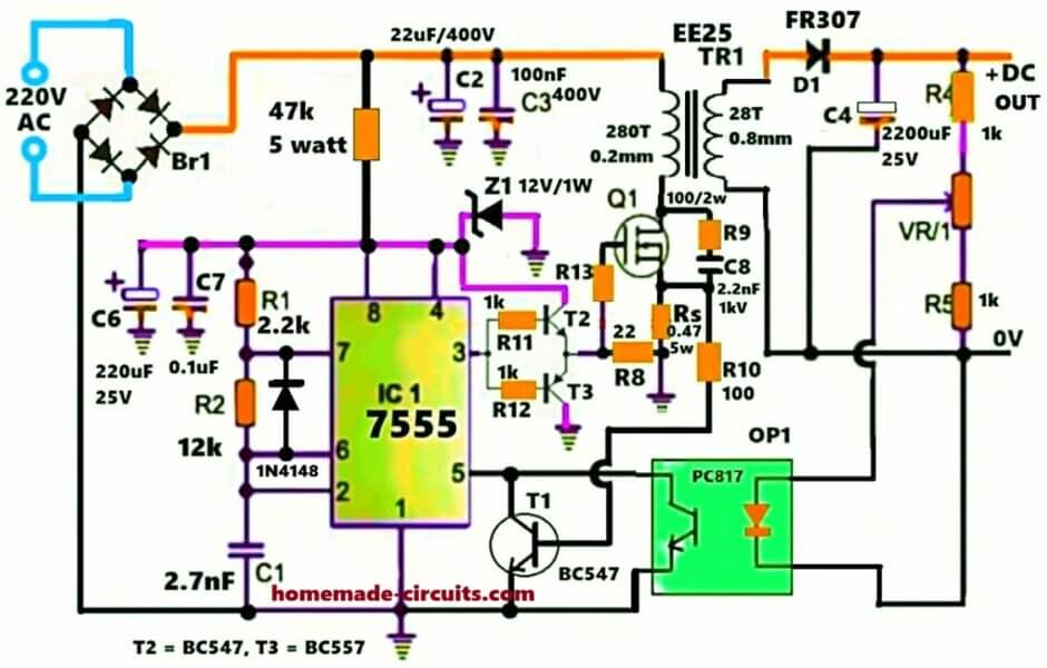
This practical flyback SMPS circuit uses ICM7555 as the main oscillator, and yep the whole idea is to take 220V AC mains directly then convert it into isolated low voltage DC through a ferrite transformer..
Unlike many PWM controller designs, here we have very few parts but still it gives mains isolation, voltage feedback, current limiting, adjustable output voltage, and that flyback energy transfer also works properly when winding is correct.
Audio/Video Representation
AC Input Rectification and High Voltage DC Section
We first feed 220V AC into bridge rectifier Br1 and then that AC becomes near 310V DC, because 220 * 1.414 gives around 311V, so now this high voltage DC becomes the main source for transformer primary side.
Across that 310V line we keep two capacitors, C2 = 22uF / 400V and C3 = 100nF / 400V because C2 handles the slower ripple from mains rectification, while C3 catches fast switching noise, so both together keep that DC line cleaner.
Circuit Diagram
Startup Supply Network
One very important part here is the 47k / 5 watt resistor, because when power first comes, then the 7555 has no supply of its own so some starting current must come first from the 310V line.
That 47k resistor lets a small current pass slowly into C6 and C7, until zener voltage builds up, so startup can begin.
If we calculate that current, then I = V / R, so 310 / 47000 gives about 6.6mA which is enough for this CMOS timer to start operaating.
Power in that resistor becomes P = V² / R, so 310² / 47000 gives near 2.04 watts, therefore 5 watt resistor is kept, since then heat stays safer over long run.
After that resistor we have Z1 = 12V / 1 watt zener which clamps supply near 12V, so the timer gets safe voltage and does not see the full high side.
Then C6 = 220uF / 25V and C7 = 0.1uF are placed there, C6 stores charge for pulse operation, C7 removes little high frequency noise, simple but necessary.
7555 Oscillator Configuration
The 7555 runs as astable oscillator using R1 = 2.2k, R2 = 12k, C1 = 2.7nF, and one 1N4148 diode across R2.
That diode matters because without it, duty cycle does not go below 50%, but here flyback needs lower ON time so the diode makes separate charge and discharge paths.
Its cathode goes to pin 7, anode goes to pins 2/6.
Frequency by formula f = 1 / (0.693 * (R1 + R2) * C1) gives near 37kHz, though in practice it sits around 35kHz to 37kHz which suits EE25 ferrite core well.
Duty by formula Duty = R1 / (R1 + R2), so 2.2 / 14.2 gives near 15.5%, therefore practical duty stays around 15%.
This low duty is good because transformer flux stays safer, MOSFET stress drops and flyback energy gets enough OFF time to release.
Flyback Transformer Primary Calculation
For primary turns we use flyback formula Np = Vin × Ton / (Bmax × Ae).
Here Vin = 300V, Bmax = 0.18 tesla, Ae = 25 × 10^-6 m², Ton = 4.28uS because 0.15 / 35000 gives 4.28 microseconds.
Then Np comes near 285 turns so practically 280 turns primary is fine.
Primary wire can be 0.2 mm enamelled copper wire, because current there is pulse type, not continuous heavy current.
Secondary Winding and MOSFET Stress
Secondary is kept 28 turns, so ratio becomes 280 / 28 = 10.
That means reflected voltage becomes 12 * 10 = 120V, so during MOSFET OFF time that 120V reflects back to primary.
Then MOSFET stress becomes 310V + 120V = 430V,therefore MOSFET must safely sit above that.
So we use IRF840 because it handles 500V drain rating.
Secondary wire can be 0.8 mm since output current can go near 1 ampere.
Output Rectification and Filtering
For output rectifier use FR307 because ordinary rectifiers get poor at 35kHz.
Then C4 = 2200uF / 25V smooths the rectified output.
Output Voltage Feedback Control
For output adjustment we use R4 = 1k, VR1 = 1k preset, R5 = 1k, and that preset changes when optocoupler starts reacting.
The optocoupler here is PC817 which sends output voltage information back to primary side while isolation stays safe.
When output rises above set level, then PC817 LED turns ON, BC547 starts acting and then 7555 control pin shifts, so pulse width reduces and output settles.
Current Limiting Through Rs Resistor
A very serious protection part is Rs = 0.47 ohm / 5 watt.
This resistor watches MOSFET source current, because when current rises then voltage appears across Rs.
This voltage across Rs, when it reaches above 0.6V, starts turning ON transistor T1 which causes pin5 of the IC 7555 to get grounded, which in turn causes the PWM width at pin3 of the IC to become proportionately narrower. This narrowing PWM causes the MOSFET to conduct less and less, until the current consumption reaches the tolerable range, in this way the max current is always kept within the tolerable range of the MOSFET.
If that voltage becomes enough, then T2 and T3 transistor side starts acting and MOSFET gate drive gets reduced.
Threshold is near 0.65V so current limit becomes I = 0.65 / 0.47 = 1.38A, meaning limiting starts near 1.3 ampere.
Without Rs, transformer may saturate, MOSFET may fail, startup surge can hit hard, so this resistor gives survival margin for the MOSFET .
Snubber Network Protection
Snubber side uses C8 = 2.2nF / 1kV, R9 = 100 ohm / 2 watt, R10 = 100 ohm.
This part catches leakage spikes, because flyback transformer always throws spike energy when switching stops.
Without snubber, drain voltage can jump too high and MOSFET safety margin can disappear.
Final Notes
With proper winding and cooling, output can reach near 12V at 0.8A to 1A.
One must keep transformer winding tight, put insulation tape between primary and secondary, keep feedback wires short, mount MOSFET on heatsink, and separate high voltage area carefully, because there the danger stays real.


Need Help? Please Leave a Comment! We value your input—Kindly keep it relevant to the above topic!