If you are wondering or worried about precisely how much power your MOSFET can tolerate under extreme conditions, or under extreme dissipative situations, then the SOA figures of the device is exactly what you should be looking at.
In this post we will be comprehensively discussing the Safe Operating Area, or the SOA, as it shows up in the MOSFET datasheet.
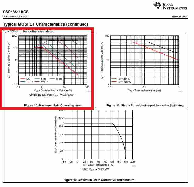
The following is the MOSFET safe operating area or the SOA graph which is normally seen in all Texas Instruments datasheets.
MOSFET SOA is described as the magnitude that specifies the maximum power the FET can handle while it's operating in the saturation region.
The magnified glimpse of the SOA graph can be see in the next image below.
In the SOA graph above we are able to see all these limitations and boundaries. And further deeper in the graph we find additional limitations for many different individual pulse duration. And these lines inside of the graph, could be determined either through calculations or physical measurements.
In earlier and older datasheets, these parameters were estimated with calculated values.
However, it is normally recommended that these parameters are practically measured. If you assess them using formulas, you could end up getting hypothetical values which may be literally much larger than the FET can tolerate in real world application. Or perhaps you may derate (over-compensate) the parameters to a level that may be way too subdued, relative to what the FET can actually deal with.
So in our following discussions I have explained the SOA parameters which are evaluated through real practical methods and not by formulas or simulations.
Let's begin by understanding what is saturation mode and linear mode in FETs.
Linear Mode vs Saturation Mode
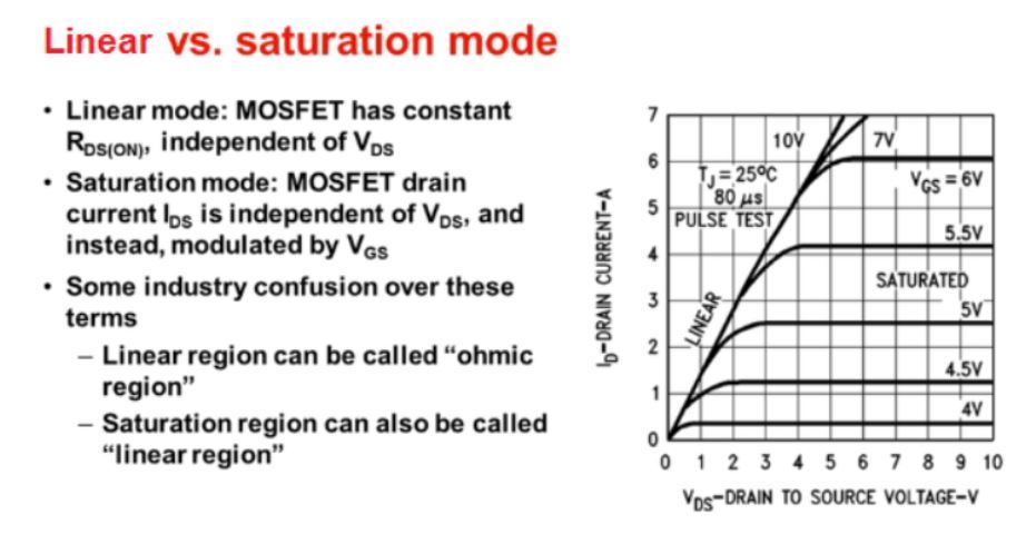
Referring to the above graph, linear mode is, defined as the region, in which the RDS(on) or the drain-source resistance of the FET is consistent.
This means, the current passing through the FET is directly proportional to the drain-to-source bias through the FET. It is also often known as the ohmic region, since the FET is essentially acting similar to a fixed resistor.
Now, if we begin increasing the drain-source bias voltage to the FET, we eventually find the FET operating in a region known as the saturation region. Once the MOSFET operation is forced into the saturation region, the current (amps) moving via the MOSFET across drain to source no longer responds to the drain-to-source bias voltage increase.
Therefore regardless of how much you increase the drain-voltage, this FET continues to transfer a fixed maximum level of current through it.
The only way through which you are able to manipulate the current is usually by varying the gate-to-source voltage.
However, this situation appears to be slightly puzzling, since these are generally your textbook descriptions of linear and saturation region. Previously I have explained that this parameter is quite often referred to as the ohmic region. Nevertheless a few folks actually name this as the linear region. Perhaps, the mindset is, well, this looks like a straight line, so it has to be linear?
If you notice folks discussing hot-swap applications, they are going to express, well, I'm working in a linear region. But that essentially is technologically inappropriate.
Understanding MOSFET SOA
Now since we know what an FET saturation region is, we can now review our SOA graph in detail. The SOA could be broken down into 5 individual limitations. I have explained what exactly they are.
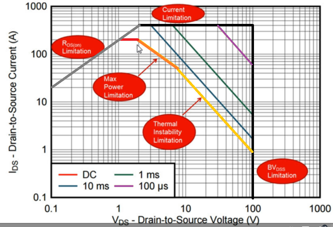
RDS(on) Limitation
The first line in the graph which is grey in color, represents the RDS(on) limitation of the FET. And this is the region which effectively limits the maximum amount of current through the FET on account of the on-resistance of the device.
In other words, it indicates the highest on resistance of the MOSFET that may exist at the maximum tolerable junction temperature of the MOSFET.
We observe that this grey line has a positive constant slope of unity, simply because each point within this line possesses an identical amount of ON resistance, in accordance to Ohm's law, which states R equals V divided by I.
Current Limitation
The next limitation line in the SOA graph represents the current limitation. Up on the graph, the different pulse values indicated by the blue, green, violet lines can be seen, limited at 400 amps by the upper horizontal black line.
The short horizontal section of the RED line indicates the package limit of the device, or the continuous current limit (DC) of the FET, at around 200 amps.
Maximum Power Limitation
The third SOA limitation is the maximum power limitation line of the MOSFET, represented by the orange sloping line.
As we notice this line carries a constant slope but a negative one. It is constant since every point on this SOA power limit line carries the same constant power, represented by the formula P = IV.
Hence, in this SOA logarithmic curve, this generates a slope of -1. The negative sign is due to the fact that the current flow through the MOSFET here decreases as the drain-source voltage increases.
This phenomenon is primarily due to the negative coefficient characteristics of the MOSFET which restricts current through device as its junction temperature increases.
Thermal Instability Limitation
Next, the fourth MOSFET limitation across its safe operating area is indicated by the yellow sloping line, which represents the thermal instability limitation.
It is across this region of the SOA which becomes really crucial to actually measure the operating capacity of the device. This is because this thermal instability region cannot be predicted by any proper means.
Therefore, we practically need to analyze the MOSFET in this area to find out where the FET may fail, and exactly what the working capability of the specific device is?
Thus we can see right now, if we were to take this maximum power limitation, and extend it all the way down at the bottom of the yellow line, then, suddenly what we find?
We find that the MOSFET failure limitation lands at the very low level, which is much lower in value compared to the maximum power limitation region promoted on the datasheet (represented by the orange slope).
Or suppose we happen to be too much conservative, and tell the people that, hey look the bottom region of the yellow line is actually what the FET can handle at the max. Well, we may be on the safest side with this declaration, but then we might have over-compensated the power limitation capability of the device, which may not be reasonable, right?
That is exactly why this thermal instability region cannot be determined or claimed with formulas, but must be actually tested.
Breakdown Voltage Limitation
The fifth limitation region in the SOA graph is the breakdown voltage limitation, represented by the black vertical line. Which is merely the maximum drain-source voltage handling capacity of the FET.
As per the graph the device features a 100-volt BVDSS, which explains why this black vertical line is enforced at 100 volts Drain-Source mark.
It would be intresting to investigate the earlier notion of thermal instability a little bit more. To accomplish this, we will need to outline a phrase referred to as "temperature coefficient".
MOSFET Temperature Coefficient
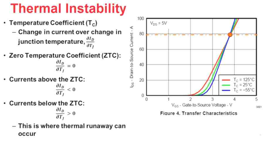
MOSFET temperature coefficient can be defined as the change in current over the change in junction temperature of the MOSFET.
Tc = ∂ID / ∂Tj
Therefore when we examine the transfer characteristics curve of a MOSFET in its datasheet, we find the drain-to-source current of the FET versus the increasing gate-to-source voltage of the FET, we also find that this characteristics is evaluated at 3 different temperature ranges.
Zero Temperature Coefficient (ZTC)
If we look at the point represented with the orange circle, this is what we'd indicate as the zero temperature coefficient of the MOSFET.
At this point even if the junction temperature of the device keeps increasing produces no enhancement in the current transfer through the FET.
∂ID / ∂Tj = 0, where ID is the drain current of the MOSFET, Tj represents the junction temperature of the device
If we look at the region over this zero temperature coefficient (orange circle), as we move from the negative -55 to 125 degrees Celsius, the current through the FET actually begins dropping.
∂ID / ∂Tj < 0
This situation is indicative that the MOSFET is really getting hotter, but the power dissipated through the device is getting lower. This implies that there's actually no danger of instability for the device, and overheating the device may be permissible, and unlike BJTs there's possibly no risk of a thermal runaway situation.
However, at currents in the region below the zero temperature coefficient (orange circle), we notice the trend, where an increase in the temperature of the device, that is, across the negative -55 to 125 degrees, causes the current transferring capacity of the device to actually increase.
∂ID / ∂Tj > 0
This happens due to the fact that the temperature coefficient of the MOSFET is at these points higher than zero. But, on the other hand an increase in current through the MOSFET, causes a proportionate increase in the MOSFET's RDS(on) (drain-source resistance) and also causes a proportionate rise in the body temperature of the device progressively, leading to further current transfer through the device. When the MOSFET gets into this region of a positive feedback loop, it may develop an instability in the MOSFET behavior.
However, nobody can tell if the above situation might happen or not, and there's no easy design for forecasting when this kind of instability might arise within the MOSFET.
This is because there may be plenty of parameters involved with the MOSFET depending on its cell density structure itself, or the flexibility of the package to dissipate heat evenly all through the MOSFET body.
Due to these uncertainties, factors like thermal runaway or any thermal instability in the indicated regions must be confirmed for each particular MOSFET. No, these attributes of the MOSFET cannot be guessed simply by applying the maximum power loss equation.
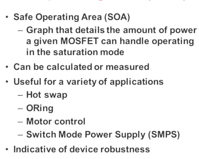
Why SOA is so Crucial
The SOA figures can be critically useful in MOSFET applications where the device is frequently operated in the saturation regions.
It is also useful in hot-swap or Oring controller applications, where it becomes crucial to know exactly how much power the MOSFET will be able to tolerate, by referring to their SOA charts.
Practically you will find that MOSFET safe operating area values tend to be very useful for most consumers dealing with motor control, inverter/converter or SMPS products, where the device is usually operated in extreme temperature or overload conditions.
Sources: MOSFET training, Safe Operating Area


Comments
Good article. Explained in simple terms. This is the only article I suppose has mentioned that, SOA is very meaningful for the MOSFET devices used in Saturation region ( Vds > Vgs- Vt). Perhaps you could have also mentioned somewhere in the article that MOSFETs are as switches only in ohmic / triode region ( Vds Vgs- Vt) region. The reason for this explicit mentioning is required due to the fact that designers use Power MOSFETs predominantly as switches. SOA is actually very handy during turn on / turn off / Hot swapping / Oring etc… along with the timing information.
By the way, the article is really good.
Best regards, Amar
Thank you very much for the useful feedback! I will surely consider your suggestions and try to include them in the article.
Excellent article- detailed enough, to the point. It certainly helps in deepening the knowledge and understanding of electronics in general.
Wishing you all the best with the future electronics projects. 😉
Thank you so much! Glad you liked the article!