If we look at the diodes, their internal construction look very simple. They are made by joining two pieces of semiconductor material, and this is called a pn-junction.
But when we talk about bipolar junction transistor or bjt, then things get little more complicated. It needs adding one more layer of semiconductor material, and that makes it special, because now it can amplify signals.
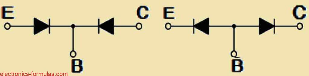
Now if we connect two single signal diodes in reverse to each other, then what we get then is two pn-junctions in series, sharing one common positive or negative terminal.
This setup makes a device with three layers, two junctions and three terminals. This becomes the basic thing of what we call bipolar junction transistor or bjt.
Transistors are very flexible parts. They have three terminals and are made from different semiconductor types.
If we give small voltage to them, then we can make them act like a conductor or like an insulator. This ability to switch between conductor and insulator makes them very useful.
Transistors do two main jobs: they work as switches which is needed in digital circuits or they amplify signals which is needed in analog circuits.
Bipolar transistors work in three main modes:
Active mode: in this mode, transistor works like amplifier where collector current (ic) is proportional to base current (Ib) times current gain (β), so IC = β*Ib.
Saturation mode: here transistor is fully switched on, works like a switch and collector current goes to maximum or saturation.
Cut-off mode: in this mode, transistor is fully off, acts as switch and no current flows through collector.
The word "Transistor" comes from mixing two words "Transfer" and "Varistor". This name shows how these small devices worked in early electronics days.
Basically transistors help to control electrical signals in circuit.
When we talk about basic bipolar transistor types, we see two types which are PNP and NPN. These names tell us how p-type and n-type materials are arranged inside.
Now let us explain how bipolar transistor looks.
It has two pn junctions and three pinouts.
We call these three terminals: emitter (E), base (B), and collector (C). Each terminal has its own job and name to help us know what is what.
Emitter (E): this is where most charge carriers come from. It pushes charges toward base.
Base (B): this is very thin layer, acts like gate to control current flow. It connects emitter and collector.
Collector (C): this terminal collects charge carriers coming from emitter.
We can think of BJT like small traffic controller for electric current. They decide how much current flows from emitter to collector based on voltage we apply to base.
So in simple way, they act like switches that we control by small current at base, and then big current flows through collector.
Here is how it works. When we send small current into base, then it lets much bigger current flow from emitter to collector.
This is why transistors are very useful because they amplify signals and control power in circuits.
Now whether we use pnp or npn transistor, both work on same basic rules.
Main difference is how we apply voltage and direction of power supply for each type.
So while they look different on paper, in real use they do same job, just small change in how we connect them.
Internal Construction of Bipolar Junction Transistors
P-N Junction Internal Structure of BJT

The Diode Analogy of BJT
BJT Symbols

How We Represent PNP And NPN Bipolar Transistors
Now let us see how we show PNP and NPN bipolar transistors and it is very simple, but we need to understand carefully. In the bipolar transistor circuit symbols, you will always find an arrow, and this arrow shows us how the current flows in the circuit, specifically from the base terminal to the emitter, so we can know direction of flow.
Now this arrow points from the positive side which is the P-type material, to negative side, which is the N-type material and it is just like it does in regular diode symbol, so you can compare easily.
How We Connect Bipolar Transistors
Because a bipolar transistor has three terminals, we have few different ways to connect it in electronic circuit and we have to choose carefully. Each setup has one terminal which acts as common point for both input and output signals, so we can share easily.
Now depending on how we connect it, the transistor reacts differently to input signal because its characteristics change based on the arrangement, and we have to remember this.
Let us see three main ways we can connect them, step by step.
Common Base Configuration: Now in this setup, we get voltage gain but we do not see any current gain, so it is like having strong signal but we cannot push much current through and we need to understand that.
Common Emitter Configuration: Now this is interesting! In this arrangement, we get both current gain and voltage gain, so it is like having powerful amplifier which boosts both strength of signal and amount of current, and we can use it in many ways.
Common Collector Configuration: Now here we get current gain without any voltage gain, so it is good for boosting current, but it does not help to increase voltage, and we must remember that.
So now depending on how we connect our transistors in circuit, we can get different results and that depends on what we need for our project, so we have to choose carefully.
Understanding The BJT Common Base (CB) Configuration
Now let us talk about Common Base (CB) setup. As name itself says, in CB setup, the Base terminal becomes shared point for both input and output signals, and we have to remember this.
So when we connect things, we apply input signal between base and emitter terminals, and we do carefully.
Then we take output signal from between base and collector terminals and now we usually ground the base or connect it to fixed voltage reference, so everything is stable.
Now let us see what happens with current in this setup. The current which flows into emitter is very big because it includes both base current and collector current, so it is more than one part.
But when we look at collector current which comes out, it is actually less than what goes into emitter, so we can see some current is “used” by base.
This means that for common base setup, we end up with current gain of “1” or even less, so it is not really amplifying current, and we have to understand that.
Now in simple way, this setup tends to reduce or "attenuate" input signal instead of amplifying it, so we can use this only when we want to reduce signal or for special case.
So even though common base setup can be useful in some situations, it does not boost current like other setups do but we can use it carefully for special things, and now we know how it works.
Analyzing The Common Base BJT Circuit

Non-Inverting Voltage Amplifier
Now let us talk about this setup. This configuration is called non-inverting voltage amplifier, and it means that input voltage (Vin) and output voltage (Vout) move together in sync so they are “in-phase,” and we can see signal follows together.
But we do not see this type of BJT configuration very often, because it has some special characteristics, especially when it comes to high voltage gain so it is not common in normal circuits.
Input And Output Behavior
Now when we look at input side, it behaves very much like forward-biased diode which means it allows current to flow easily, so signal goes in without much block.
On output side it works just like little photo-diode which is sensitive to light, and we can see it reacts to small changes easily, so it is very sensitive setup.
Resistance Gain
Another interesting thing about this setup is that it has very high ratio of output resistance to input resistance and this is important because it gives us what we call “Resistance Gain,” so it can make signal stronger in special way.
Now we can say that load resistance RL is much higher compared to input resistance Rin, which is important feature of this configuration so it works like amplifier in careful way.
Voltage Gain
Now when we calculate voltage gain Av for this common base configuration, we can see how effectively it amplifies the signal, and we can use it to understand behavior of circuit.
So overall, even though this type of amplifier circuit is not very common, it definitely has special traits which can be useful in certain situations, and now we can see why it is important to know about it.
Formula For Calculating BJT Common Base Voltage Gain
Now let us see the formula for BJT Common Base voltage gain. We write it like this:
Av = Vout / Vin = (IC * RL) / (IE * RIN)
In this formula IC / IE refers to current gain which is also shown by symbol alpha α, and RL / RIN refers to resistance gain of the BJT so we can understand both parts.
Now because of this formula, when we talk about common base circuit, we usually see it being used in simple amplifier setups, like for microphones or radio frequency (Rf) stuff and we use it because it does very good job at handling high frequencies so it is special.
Understanding The Common Emitter (CE) BJT Configuration
Now let us look into Common Emitter (CE) setup. In this setup, we put input signal between base and emitter and then we take output from between collector and emitter, so we get input and output separated clearly.
This setup is actually most popular way to connect transistors for amplifiers, and it is what we think of as standard method for bipolar transistors, so almost everyone uses this.
What is cool about Common Emitter amplifier setup is that it gives us best current and power gain compared to the other two configurations we have with bipolar junction transistors, so it is very powerful.
The reason is because it has LOW input impedance, since it connects to forward biased PN-junction, and we can easily drive small signal into it.
But on the other side it has HIGH output impedance, since it comes from reverse biased PN-junction so it can push strong signal out.
So in simple way, this setup really maximizes gain of amplifier design and we can use it for most amplifier applications, now we understand why it is popular.
Analyzing The BJT Common Emitter Amplifier Circuit

Now let us start slowly. In a BJT common emitter amplifier circuit, we must remember that the current which is flowing out of the transistor has to be exactly equal to the currents which are going inside the transistor.
So we can think like this. The emitter current which we call Ie is made from two parts. We can write like this: Ie = Ic + Ib.
What Happens With Load Resistance
Now let us say we connect a load resistance RL in series with the collector. Then what happens is that the current gain for this common emitter transistor becomes very big.
This gain is ratio of Ic, which is the collector current, to Ib, which is the base current. We represent this current gain by a Greek letter Beta, and it looks like β.
Understanding Alpha
So since we already know that emitter current is written as Ie = Ic + Ib, we can also define another ratio. We call it Alpha and it is written with Greek letter α.
This Alpha is equal to Ic/Ie. Now it is very important to note that Alpha is always less than one. It will never become equal to one.
Relationship Between Ib, Ic, And Ie
Now here is interesting point. The relationship between Ib, Ic, and Ie depends fully on how the transistor is physically built.
This means that if we make even a very small change in base current Ib, then we will see a much bigger change in collector current Ic.
So basically when we adjust current flowing into base just little, then it controls how much current flows through emitter and collector.
Typical Values Of Beta
Now for most general-purpose transistors, Beta usually stays between 20 and 200.
So let us take one transistor with Beta value equal to 100. Then it means that for every one electron that flows from base terminal, almost 100 electrons flow between emitter and collector terminals.
Relation Between Alpha And Beta
Finally if we combine expression of Alpha α and Beta β then we can make a mathematical relation which joins these two parameters together, and this relation gives us idea about current gain of our transistor as seen below.
Alpha, (α) = IC/IE and Beta, (β) = IC/IB
∴ IC = α * IE = β * IB
Since we have, α = β/(β + 1), and β = α/(1 - α)
∴ IE = IC + IB
Understanding The BJT Common Emitter (CE) Configuration
In the above formula the Ic indicates the current flowing into the collector terminal, the Ib represents the current flowing into the base terminal, and the Ie denotes the current flowing out of the emitter terminal.
So now, when we are talking about this type of bipolar transistor configuration, we can say that it has very impressive input impedance. Along with that, it also has high current gain and power gain compared to what we see in the common base configuration. But one bad thing is that its voltage gain becomes quite lower, and we must remember that.
Another important point is that the common emitter configuration works like an inverting amplifier circuit.
What this means is that the output signal that we get will have a phase shift of 180 degrees compared to the input voltage signal. So if we supply an input signal to this configuration then the output becomes flipped upside down or inverted, and this is the main property.
Understanding The BJT Common Collector (CC) Configuration
Now let us talk about the Common Collector (CC) setup. In this configuration, which we also call as the grounded collector configuration, we connect the collector pin of the BJT with the ground supply line of the power supply. So this means the collector terminal becomes common for both the input signals and the output signals, and this looks good.
Now when we see the connection details then we find that the input signal goes directly to the base terminal.
Next we take the output signal from across the emitter load resistor, just like it is shown in diagrams.
This type of configuration is very often called a Voltage Follower or an Emitter Follower circuit, and we must know that.
One very useful thing about this common collector or emitter follower setup is how it works in impedance matching applications.
It gives us very high input impedance, sometimes in the range of hundreds of thousands of Ohms. At the same time, it keeps the output impedance quite low and this makes it very effective.
So in short, a common collector BJT circuit becomes a fantastic choice when we want to match impedances in our electronic circuits and that is why we use it often.
Analyzing a Common Collector BJT Circuit Design

Common Emitter Configuration
Now let us talk about common emitter configuration step by step. We see that it has a current gain, and that current gain is almost equal to the β value of the transistor itself. So we can say that this is quite simple for us to understand.
Common Collector Configuration
Now let us see common collector configuration. Here we can see that the load resistance gets connected in series with the emitter terminal of the BJT. That means the current which is flowing through this configuration is actually equal to the emitter current, and we need to note this carefully.
Emitter Current Relation
Now here it becomes little more interesting for us. The emitter current is not alone. It is actually made up of both the collector current and the base current all added together, so we can see that it is a mix.
So in this type of transistor configuration, the load resistance finally has both the collector current and the input current from the base flowing through it, and this is how it works.
Defining The Current Gain
Now by using all the above facts, we can define the current gain of this circuit through the following formulas:
IE = IC + IB
Ai = IE/IB = (IC + IB)/ IB
Ai = IC/IB + 1
∴ Ai = β + 1
Common Collector Current BJT Configuration
Now we see that the common collector current BJT configuration is taken as a non-inverting circuit. That means the input signal voltage Vin and the output signal voltage Vout are actually in-phase. So when we look at input and output voltages then we find that both move together in same direction, like harmony.
Voltage Gain Of Common Collector
Now when we check more about common collector configuration then we see that it has voltage gain almost equal to 1. We call this unity gain, so it is like no extra voltage amplification.
Because of this special thing, we can also think that this circuit works like a voltage buffer, since it keeps voltage gain right at unity, so no loss and no extra.
Load Resistance Behavior
Now in this configuration, the load resistance of common collector transistor receives both the base current and the collector current that flow through it.
So this action gives us large current gain. It is very similar to what we saw in common emitter configuration, so here also we get good current amplification. But voltage gain stays very small, almost nothing more than unity.
Summary Of Configurations
Now that we have checked carefully these three different types of bipolar transistor configurations, then we can summarize clearly. We will put all the relations between the individual DC currents that flow through each leg of BJT, and also their respective DC current gains.
So we can present all this information in a simple table, so we get clarity and understanding.
Table Showing the Relationship between the DC Currents and the Gains of BJT Configurations
| Equation | Description |
|---|---|
| IE = IB + IC | Kirchhoff's Current Law (KCL) applied to a transistor: Total emitter current (IE) equals the sum of base current (IB) and collector current (IC). |
| IC = IE - IB | Rearranged KCL equation: Collector current (IC) is the difference between emitter current (IE) and base current (IB). |
| IB = IE - IC | Rearranged KCL equation: Base current (IB) is the difference between emitter current (IE) and collector current (IC). |
| α = IC / IE | Definition of alpha (α): Current gain from emitter to collector. |
| β = IC / IB | Definition of beta (β): Current gain from base to collector. |
| IC = β * IB | Relationship between collector current (IC) and base current (IB) using beta (β). |
| IE = (1 + β) * IB | Relationship between emitter current (IE) and base current (IB) using beta (β). |
| IB = IC / β | Relationship between base current (IB) and collector current (IC) using beta (β). |
| IE = IC / α | Relationship between emitter current (IE) and collector current (IC) using alpha (α). |
How Transistor Works With Connection
Now let us see. When we use a transistor, whether it is NPN or PNP, the way we connect it with other parts decides how the signal will get amplified. So we can say the connection style is very important.
The calculation for how much signal is amplified is same for both NPN and PNP transistor, so we do not have to change the formula.
Difference Between NPN And PNP
The only difference between NPN and PNP is that the current flow direction and the polarity of voltages become opposite. So even though calculation is same, the actual voltage and current go in opposite direction for NPN and PNP.
Conclusions
Now let us make conclusion. How the transistor behaves inside a circuit depends on how we connect it. Since there are different connection types, that will change how much the circuit can amplify, how much resistance it shows at input and output, and how much power it can gain.
The table below gives us the differences for each transistor configuration. So, depending on what we want our BJT circuit to do, we can choose the configuration that gives us correct combination of input resistance, output resistance, and gain.
Table showing Different types of Bipolar Junction Transistor Configurations and their Characteristics

| Characteristic | Common Base | Common Emitter | Common Collector |
| Input Impedance | Low | Medium | High |
| Output Impedance | Very High | High | Low |
| Phase Shift | 0o | 180o | 0o |
| Voltage Gain | High | Medium | Low |
| Current Gain | Low | Medium | High |
| Power Gain | Low | Very High | Medium |
References:


Comments
sir, your common base configuration is wrong. there is positive and negative both supplies are connected to base it will short to the transistor immediately, secondly I don’t understand those configurations more deeply do you have any other idea or I mean way to understand those configurations easily. I don’t know why in common collector configuration there is added load to emitter and what if there is pnp transistor in cc configuration,then where it to connect load.please explain in simple words.thanx
Hey Atul, There is no short circuit here. The base is not directly connected to both supplies. This is a conceptual bias diagram, not a literal wiring layout. In real circuits, current is always limited by resistors or signal sources.
To understand transistor configurations easily, just remember which terminal is common:
Common Base: Base is fixed, input at emitter, output at collector.
Common Emitter: Emitter is fixed, input at base, output at collector.
Common Collector: Collector is fixed, input at base, output at emitter.
In common collector, the load is connected to the emitter because the emitter voltage follows the base voltage.
For a PNP transistor, the idea is the same, only the polarities are reversed. The load is still connected to the emitter.
The confusion comes from reading a theory diagram as an actual wiring diagram.
thanks very much sir, I’m very obliged. sir please can you send me any article on actual wiring diagram to know those configurations deeply and easily.
You are welcome Atul,
You can easily find the practical versions of these circuits online, with explanations, simply by searching the following phrases:
“Common Base BJT amplifier circuit diagram”
“Common Emitter BJT amplifier circuit diagram”
“Common Collector BJT amplifier circuit diagram”