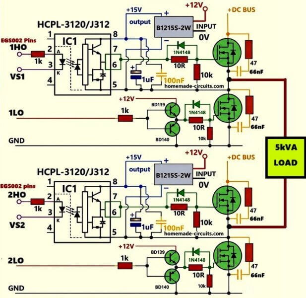
In this article I will explain how to upgrade an EGS002 inverter board to 5kVA power level using the HCPL-3120 or HCPL-J312 opto isolated drivers with isolated inputs and isolated power supply stages. However, the low side MOSFETs are driven through ordinary BJT totem pole configuration such as by using BD139 and BD140 transistor pairs.
Circuit Diagram
Basic Working Concept
Whole thing is meant for driving a full H-bridge from high voltage DC bus line, so now both upper and lower sections together make the complete inverter bridge.
Upper side handles one half bridge, lower side handles the other half, and both sides work opposite to create AC waveform at output.
Main blocks here are EGS002 SPWM outputs, HCPL isolated driver side, isolated DC-DC supply, high side gate drive section, low side transistor driver, MOSFET bridge stage, then those snubber parts and gate protection components around MOSFETs.
Audio/Video Representation
EGS002 Control Signals

The EGS002 gives four outputs mainly, 1HO, 1LO, 2HO and 2LO.
1HO and 2HO are for high side MOSFET drive, while 1LO and 2LO go toward low side driver stage. These outputs are complementary SPWM pulses, so when one side switches then the opposite side stays OFF.
VS1 and VS2 are floating reference points for the high side driver side.
Those 1k resistors connected to HCPL inputs are simply current limiting resistors for the internal LED side.
HCPL-3120 / HCPL-J312 High Side Driver
The HCPL-3120 or HCPL-J312 is very common in inverter gate driver circuits because it gives isolation and strong gate drive current together.
Inside it we basically have LED section, optical isolation barrier, and gate driver output stage.
When EGS002 sends pulse through that 1k resistor into pin 2 side then internal LED switches ON, which activates output stage inside the IC, and then MOSFET gate gets driven.
Now high side MOSFET source never stays fixed, sometimes near 0V, sometimes near full DC bus voltage, so gate driver also has to float together with it, otherwise direct controller connection can damage the low voltage side very fast.
That is why this optical isolation becomes important here.
Isolated DC-DC Converter
That small B1215S-2W module is isolated DC-DC converter.
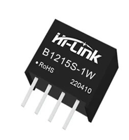
It takes normal +12V and 0V from control side, but output side gives isolated floating +15V supply for HCPL driver section. Without this floating supply then high side gate driver cannot move with MOSFET source voltage properly, so circuit will not work correctly.
High Side MOSFET Gate Drive Section
Upper MOSFET in each bridge side is the high side MOSFET, and HCPL output drives its gate through 10 ohm resistor and 1N4148 diode arrangement.
That 10 ohm resistor helps limit sudden gate charging current, also reduces ringing and EMI a bit...
The 1N4148 diode makes gate charge and discharge speeds different from each other, so one direction becomes faster. Usually faster discharge is preferred because it helps reduce shoot through risk.
Gate Pull Down Resistors
Each MOSFET gate has one 10k resistor connected between gate and source. This keeps MOSFET safely OFF during startup or noise conditions, because MOSFET gates can sometimes turn ON accidentally from floating charge.
Low Side MOSFET Driver Stage
Low side MOSFETs are driven using BD139 and BD140 complementary transistor pair. This section acts like push pull gate driver.
1LO and 2LO outputs from EGS002 enter this transistor pair through 1k base resistors.
Transistor pair gives stronger current amplification compared to driving MOSFET gates directly, therefore gate charging and discharging become much faster.
When input signal goes HIGH then BD139 conducts and MOSFET gate charges quickly.
When signal goes LOW then BD140 conducts and gate gets discharged fast.
MOSFET Bridge Configuration
All four MOSFETs together form the full H-bridge stage.
Bridge keeps switching DC bus voltage across load in opposite directions repeatedly, and because EGS002 produces SPWM waveform then after transformer and filtering we get sine wave AC output.
RC Snubber Network
Across each MOSFET there is 47 ohm resistor and 66nF capacitor connected in series, which forms RC snubber network.
These parts absorb voltage spikes and switching transients, especially transformer leakage spikes which can become dangerous in high power inverter systems. So now MOSFET stress reduces, ringing reduces, EMI reduces, and reliability improves then.
Capacitors Near HCPL Driver
Near isolated supply side, see that 1uF electrolytic capacitor and 100nF ceramic capacitor. These are bypass capacitors for supply stabilization.
100nF capacitor mainly filters high frequency switching noise, while 1uF capacitor supplies local pulse current storage for the gate driver section. Both of them together help HCPL driver stay stable during fast switching.
Overall Working Principle
Working is actually not too complicated actually.
- EGS002 creates SPWM pulses first.
- HCPL drivers isolate and amplify high side pulses.
- BD139 and BD140 stages strengthen low side pulses.
- Then MOSFET bridge switches DC bus alternately across load.
- After transformer and filtering, SPWM waveform becomes sine wave AC output.
Why This Design Works Well For High Power
This driver stage is good for higher power inverter systems because gate drive current is strong, high side isolation is proper, MOSFET switching stays fast and switching losses get reduced.
Noise immunity also becomes better and chances of shoot through reduce if dead time is adjusted correctly.
Important Practical Notes
Dead time setting inside EGS002 is very important because if both MOSFETs turn ON together even for tiny moment then shoot through current can destroy MOSFETs very quickly.
PCB layout also matters a lot here.
Gate tracks should stay short, copper tracks should be thick, signal ground and power ground should not mix carelessly and bypass capacitors should be very close to driver ICs.
For 5kVA operation MOSFETs should have lowest RDS(on), high current rating, fast switching capability and proper voltage margin, otherwise heating and switching losses can rise badly.
Conclusion
This is actually one solid and practical MOSFET driver stage for 5kVA sine wave inverter systems using EGS002 controller.
HCPL-3120 drivers safely handle isolated high side driving while BD139 and BD140 pair gives strong low side gate drive current.
Together the whole stage switches the full bridge MOSFET section quite efficiently, and protection against spikes, noise and switching stress also becomes reasonably good.


Questions & Answers
I am pleased to be able to draw upon your exceptional expertise. Please take a look at this circuit and let me know if I have designed it correctly regarding battery voltage drop and overcurrent protection.However, I was unable to upload the designed PCB for you
Please send the diagram to my email ID, I will check it and reply you here:
homemadecircuits
@gmail.com
Hola amigo me gustaría saber si tiene un ocb diseñado para está adaptación a la tarjeta egs002. Gracias
Hi, sorry, no I do not have a PCB design for this project…