The following useful circuit of a TV antenna amplifier was sent to me by an avid reader of this blog Mr. Miljenko Farkas. I am extremely grateful to him for his kind contribution to this site.
Here's what he wrote in his email:
I've sent you a schematic of a TV antenna amplifier that can assist boost reception in places with poor signal strength or under challenging TV signal circumstances.
Although this amplifier has performed admirably in Europe I'm not sure how well it would function elsewhere.
This is an opportunity to test it out since I believe certain designers could find it to be an intriguing challenge. The amplifier should be placed at the top of the antenna once it is constructed and the power supply or rectifier circuit should be near the television.
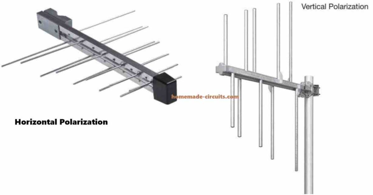
Both vertical and horizontal logarithmic antenna types are supported by the amplifier's architecture.
There is just one power line that runs from the TV to the antenna which supplies both power and signal and both antennas can connect to the amplifier simultaneously.
That concludes this year. I hope 2025 brings you nothing but the finest!
Overview
So this antenna amplifier is made to really enhance how well your TV picks up signals especially in spots where the signals are kind of weak or just hard to get.
It works with two different kinds of polarization for logarithmic antennas which are vertical and horizontal. What it does is take the signals from both types and merges them into a single coaxial cable. This cable is responsible for carrying not just the boosted signal but also the power supply that the amplifier needs to work.
Now when it comes to where you should put this amplifier for it to work its best you want to place it really close to the antenna. This setup helps it do its job efficiently. Meanwhile the rectifier and power supply should be set up near your TV so everything runs smoothly.
Circuit Working
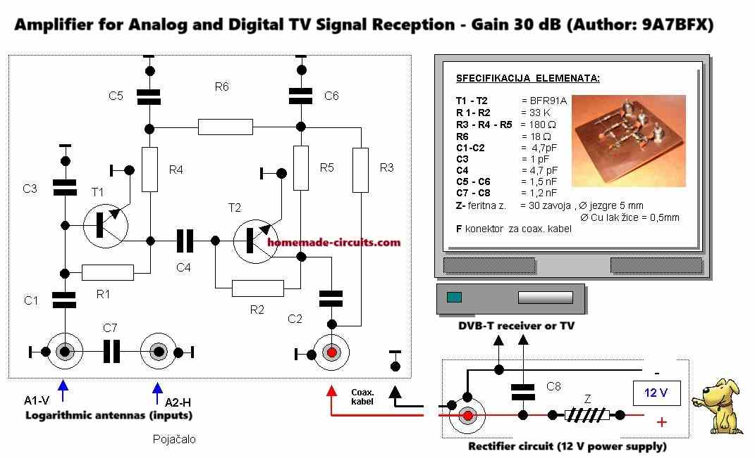
Amplifier Section Transistors (T1 and T2 - BFR91A):
These are high-frequency NPN transistors commonly used in RF amplifiers.
T1 and T2 form a two-stage amplifier.
The signal from the antennas is fed to T1, amplified, and passed to T2 for further amplification.
This cascading increases the overall gain, ensuring a 30 dB signal boost.
Capacitors (C1, C2, C3, C4, C5, C6):
C1 and C2 work like coupling capacitors passing the high-frequency signal while blocking DC components.
C3 and C4 are the bypass capacitors which stabilize the DC operating points of T1 and T2 by shorting high-frequency noise to ground.
C5 and C6 are used to fine-tune the circuits frequency response optimizing it for TV signal frequencies.
Resistors (R1 to R6):
R1 and R2 are the biasing resistors for the transistors for setting the operating point for stable amplification.
R3, R4, and R5 are the load resistors which determes the gain of each transistor stage.
R6 is the current-limiting resistor for ensuring proper current flow to the transistors.
Ferrite Core Inductor (Z):
A small inductor with 30 turns on a 5 mm core.
Acts as an impedance-matching element, ensuring minimal signal loss when interfacing with the coaxial cable.
Dual Input (A1-V and A2-H):
The circuit supports two separate logarithmic antennas for vertical (A1-V) and horizontal (A2-H) polarization.
These antennas are connected in parallel to the amplifier, enabling simultaneous reception of both polarizations.
Power Supply Section C7 and C8:
Act as DC filter capacitors to stabilize the power supply voltage.
Smooth out any ripples from the rectifier circuit to ensure clean power to the amplifier.
Coaxial Cable (Signal + Power):
A single coaxial cable carries both the amplified signal and the 12 V DC power supply to the amplifier.
The power is extracted at the amplifier end, while the signal is passed to the TV at the other end.
Rectifier Circuit:
Located near the TV this circuit converts AC from the mains to DC providing us the required 12 V for the amplifier.
Main Points for Installation Amplifier Placement:
The amplifier must be installed at the top of the antenna to minimize the signal loss from cable resistance and interference.
Power Line Sharing: The coaxial cable does two things, it powers the amplifier and also transmits the amplified signal back to the TV or receiver.
Compatibility: The circuit has been tested successfully in Europe wherein the TV signal frequencies and standards might be different.
Testing throughout outside the Europe is encouraged to verify the compatibility with other regional broadcasting standards.
Applications and Challenges Applications: This amplifier could be highly useful for the rural or the remote areas wherein TV signals are weak due to distance or obstacles.
Challenges: If used outside the Europe then the amplifier’s components might need some adjustment to match different regional TV frequency bands.
For example the values of the C5, C6, and Z might need tweaking some.
This circuit provides an interesting and practical solution for improving the TV reception and it gives a great opportunity for enthusiasts to experiment and adapt it to their specific needs...
I am an electronics engineer and doing practical hands-on work from more than 15 years now. Building real circuits, testing them and also making PCB layouts by myself. I really love doing all these things like inventing something new, designing electronics and also helping other people like hobby guys who want to make their own cool circuits at home.
And that is the main reason why I started this website homemade-circuits.com, to share different types of circuit ideas..
If you are having any kind of doubt or question related to circuits then just write down your question in the comment box below, I am like always checking, so I guarantee I will reply you for sure!
I want your help with my understanding of how this circuit works. Its too bad you didn’t draw it, but maybe we can both learn something.
I begin with the power supply of 12V coming from near the television set. The power goes into the amplifier board and it charges C2 and it supplies current through R3 which is held up by C6. The current/voltage/power goes through R5 and into the PNP (T2) collector where it opposes the charge on C2 and also provides power through R2 to the base of T2 that will only be effected by changes in signal because of C4. The 12V power also goes through R6, is held up by C5, is connected to the collector of T1, and goes down through R4 were it meets the other side of C4 and goes through R1 to the base of T1. Now I come to the antenna input.
A1-V and A2-H cause the base of T1 to follow the radio signal. The voltage and current at C4 fluctuates because of that signal at T1’s base and because power is gated from the R1,C4,R4 junction through T1 by the gate/antenna signal. That is the first stage of amplification. At T2 from the other side of C4 the second stage works the same way and C2 opposes the 12V on the antenna to TV cable. Because of the values of the resistors and capacitors I assume the center of the signal returning to the TV through the cable is at 0 volts. So in operation, the only current that flows through the TV to amplifier cable and thus the voltage that corresponds to it is never really at 12 volts but is only at the amplified voltage of the radio signal.
I am wondering what you think of my view of how this works and what you would say or point out if I had said to you. Thanks for any help. This is one of the few circuits I could find that have the power in line instead of separate. Thanks for supplying the circuit and I hope to learn from your comments about where I have the wrong view of how this circuit is working or what words you use instead of those I used.
Here is another attempt to analyze the circuit. I still cannot conclude I understand it.
First I follow the power through the circuit:
The current comes in to C2 (4.7pF) and creates a ground on the other side of C2 at the collector of T2. The current goes to R3 that is a 180Ω leaving 12V/180Ω=0.067A or 67mA and that reaches C6 (1.5nF) to charge it. The same current then goes through R5 that is 180Ω leaving 12V/360Ω = 33.3mA and that goes to the collector of T2 (BFR91A), but the voltage also goes on to R2 that is 33K and that current is 12V/33360Ω leaving 360μA at the base of T2. The emitter of the NPN T2 is grounded. The 12V also goes to R6 (18Ω) that is 198Ω leaving 60.6mA at C5 (1.5nF) the other side being grounded. That current goes on into R4 (180Ω) leaving 12V/378Ω = 31.7mA at the collector of T1 (BFR91A) that appears at C4 (4.7nF) and at R1 (33K) continuing as 12V/33378 = 360μA to the base of T1 and at the positive side of C3 (1pF) and on one side of C1 (4.7pF) the other side of which is the antenna jack.
I simplify slightly:
For the sake of simplicity I am going to eliminate C7 (1.2nF) and A2-H, but if I did not C7 shows the same as the antenna side of C1 (4.7pF).
Now I analyze from the Antenna:
Suppose the signal strength at the antenna is 10μA and that is a weak signal since S meters are full scale at 50μA to 100μA. C1 is a 4.7pF. Assuming the antenna has 400mΩ of resistance and I is 10μA then, since I = V/R V = IR = 10μA * 100mΩ = 1μV. RC is then 4.7E-13. If I had 1.0E-1 that number would be 0.1. If I then wanted to display it with exponential notation it would be 0.1E0 so I could add 1 to the exponent and move the decimal point to the right. Therefore 4.7E-13 becomes 47E-12 and that is 47 picoseconds. The capacitor is thus charged fully in 5RC or 2.35E-10 or 23.5E-9 or 23.5 nanoseconds. If the frequency were 100MHz, since that is in the FM band, each wave time would be 100E6-1 = 10 nanoseconds (10ns). So at that frequency the capacitor does not fully charge. As it does charge it could be said to push positive charges out the other side of C1 (4.7pF) or to push negative charges out the other side depending on which side of the wave the antenna was receiving. When it does so it effects the current at R1 (33K) and it effect the charge on C3 (1pF) as well as at the base of T1. What I believe is desired is that the base of T1 is on as the signal fluctuates between positive and negative from the antenna. The datasheet of T1/T2/BFR91A does not show me the conductivity of the collector emitter at different base voltages and currents, but I know a transistor does not turn on until 0.6 volts. The current at R1 was 360μA but the voltage at R1 is not ground since it does not connect to ground and there is the potential voltage difference of 1μV. Common sense tells me the voltage is being supplied by the 12V supply and without a ground in this resistor voltage ladder I could expect 12V but for the ground to the emitter of T1. With a β of 120 from the datasheet I could guess the 360μA becomes 43.2mA flowing to ground through the emitter when T1 is fully on, but there is not that much current available there since only 31.7mA is coming out of R4. I would guess that at 12V and 31.7mA through the collector emitter that T1 would not be over its wattage rating that is 2Watts as when there is no radio signal since no antenna is plugged in. I would also believe T1 should be in the flat part of its amplification curve rather than in the linear region not only because the base voltage is at about 12V but because I want uniform amplification of all frequencies through T1. Only the antenna signal should be amplified, but I do not know the amplification curve looks, so I can assume it is working at 12V and there is only a very small change caused by the antenna signal. That small change will appear at C4 (4.7pF) and the second stage amplifies more than the first at T2. That amplification appears on C2 (4.7pF) and on the Jack that goes back to the radio or television.
I summarize:
Unfortunately, I cannot predict the frequency range this circuit will operate within except assuming that TV signals go from 40MHz to 200MHz in Eastern Europe and that this circuit originated in Eastern Europe. The author suggested C5 (1.5nF) and C6 (1.5nF) might need tweaking to improve performance outside of Eastern Europe. It seems to me the capacitors absorb current and provide current to the circuit at a specific rate and that rate effects whether the circuit can reproduce the amplified signal or if it will be distorted.
Thank you very much for your deep analysis. I greatly appreciate it.
However, it can be quite time consuming for me to go through all the calculations you have provided, so instead I will try to simulate it in the following simulator whenever i am free or have time. I will let know the results once done…: https://www.homemade-circuits.com/circuit-simulator/
Thank you,
I know it is so much work to analyze this circuit that I never did expect you to do it. I thought perhaps somebody who was a professional at this or somebody who knew something that I obviously had missed might comment over time. I believe I might get it someday and I appreciate being able to do it in public where others can comment and help. The original article was published in January and I was the only post in July so far, so these things take a lot of time.
That simulation is really going to be great if you are able to do it, I will be using that!
It seems now the link not opening after doing all the hard work…I should have made a video instead.
But in the simulation I could see the output nicely oscillating with -12V AC output…
Although the comment has not been approved yet for posting,
I can’t get my simulation (that I provided the link to) in kicad to work. I get a signal though but it is not amplified. I tried putting a resistor at the output, and I tried an inductor, but it still does not amplify. Its not far from working but this is a lot of work and its a holiday.
The picture shows the circuit, but I can only post one picture.
It has the kicad project file and the simulator is built into kicad (its free software), the only other file necessary being the BFR93AW_SPICE.PRM file for the transistor that does include the BFR91A model in it. To assign that model highlight the transistor and use the (right click) “Properties…” menu item to get to the properties screen. At the bottom there is a button that is “Simulation model” where the file name BFR91A can be placed. That is all it seems to need, the model pull down does nothing. After that the simulator can be run from the “Inspect” top toolbar menu and “simulator” beneath it.
My link now actually opens when I use a short-link. You can check it here: https://shorturl.at/jv1Ow
I do not know kicad, so I cannot operate your simulation, moreover your link is taking me to an unsecured page.
That movie or video works for me, the shorturl still does not, but I did see the simulation. Thanks very much for the movie and I think I can get that kicad spice simulator to work some day, but I am not sure when.
Ok no problem. However, I think you should try pasting the short URL in chrome “guest mode” which is available in your standard chrome browser itself. Currently it might not be working for you because of cache, and guest mode does not store any cache and so the URL should work.
Anyway, if the video has solved the problem, then no need for this.
Your kicad simulation could be good, but the link is not secured, so you should make your website an https, in order to make it secured.
Here’s the simulation link, you can check it and do any necessary tweaks if required: https://shorturl.at/jv1Ow
Thank you Todd, for analyzing this circuit deeply. It is much appreciated.
Your explanation is quite correct, but according to me the final amplification happens by oscillating the full 12V into the TV input by T2. So the modulated amplified signal corresponds to 12v oscillations which is fed to the TV circuit.
As you can see the 12V DC is connected directly C8, so when T2 oscillates, it correspondingly switches this 12V through C2, which is then fed to the TV circuit via C8. Here’s a better view of the circuit when it is rotated upside down. https://www.homemade-circuits.com/wp-content/uploads/2025/07/TV-antenna-amplifier-circuit.jpg


Comments
I want your help with my understanding of how this circuit works. Its too bad you didn’t draw it, but maybe we can both learn something.
I begin with the power supply of 12V coming from near the television set. The power goes into the amplifier board and it charges C2 and it supplies current through R3 which is held up by C6. The current/voltage/power goes through R5 and into the PNP (T2) collector where it opposes the charge on C2 and also provides power through R2 to the base of T2 that will only be effected by changes in signal because of C4. The 12V power also goes through R6, is held up by C5, is connected to the collector of T1, and goes down through R4 were it meets the other side of C4 and goes through R1 to the base of T1. Now I come to the antenna input.
A1-V and A2-H cause the base of T1 to follow the radio signal. The voltage and current at C4 fluctuates because of that signal at T1’s base and because power is gated from the R1,C4,R4 junction through T1 by the gate/antenna signal. That is the first stage of amplification. At T2 from the other side of C4 the second stage works the same way and C2 opposes the 12V on the antenna to TV cable. Because of the values of the resistors and capacitors I assume the center of the signal returning to the TV through the cable is at 0 volts. So in operation, the only current that flows through the TV to amplifier cable and thus the voltage that corresponds to it is never really at 12 volts but is only at the amplified voltage of the radio signal.
I am wondering what you think of my view of how this works and what you would say or point out if I had said to you. Thanks for any help. This is one of the few circuits I could find that have the power in line instead of separate. Thanks for supplying the circuit and I hope to learn from your comments about where I have the wrong view of how this circuit is working or what words you use instead of those I used.
I see that the transistors are NPNs and not PNPs! Sorry.
Here is another attempt to analyze the circuit. I still cannot conclude I understand it.
First I follow the power through the circuit:
The current comes in to C2 (4.7pF) and creates a ground on the other side of C2 at the collector of T2. The current goes to R3 that is a 180Ω leaving 12V/180Ω=0.067A or 67mA and that reaches C6 (1.5nF) to charge it. The same current then goes through R5 that is 180Ω leaving 12V/360Ω = 33.3mA and that goes to the collector of T2 (BFR91A), but the voltage also goes on to R2 that is 33K and that current is 12V/33360Ω leaving 360μA at the base of T2. The emitter of the NPN T2 is grounded. The 12V also goes to R6 (18Ω) that is 198Ω leaving 60.6mA at C5 (1.5nF) the other side being grounded. That current goes on into R4 (180Ω) leaving 12V/378Ω = 31.7mA at the collector of T1 (BFR91A) that appears at C4 (4.7nF) and at R1 (33K) continuing as 12V/33378 = 360μA to the base of T1 and at the positive side of C3 (1pF) and on one side of C1 (4.7pF) the other side of which is the antenna jack.
I simplify slightly:
For the sake of simplicity I am going to eliminate C7 (1.2nF) and A2-H, but if I did not C7 shows the same as the antenna side of C1 (4.7pF).
Now I analyze from the Antenna:
Suppose the signal strength at the antenna is 10μA and that is a weak signal since S meters are full scale at 50μA to 100μA. C1 is a 4.7pF. Assuming the antenna has 400mΩ of resistance and I is 10μA then, since I = V/R V = IR = 10μA * 100mΩ = 1μV. RC is then 4.7E-13. If I had 1.0E-1 that number would be 0.1. If I then wanted to display it with exponential notation it would be 0.1E0 so I could add 1 to the exponent and move the decimal point to the right. Therefore 4.7E-13 becomes 47E-12 and that is 47 picoseconds. The capacitor is thus charged fully in 5RC or 2.35E-10 or 23.5E-9 or 23.5 nanoseconds. If the frequency were 100MHz, since that is in the FM band, each wave time would be 100E6-1 = 10 nanoseconds (10ns). So at that frequency the capacitor does not fully charge. As it does charge it could be said to push positive charges out the other side of C1 (4.7pF) or to push negative charges out the other side depending on which side of the wave the antenna was receiving. When it does so it effects the current at R1 (33K) and it effect the charge on C3 (1pF) as well as at the base of T1. What I believe is desired is that the base of T1 is on as the signal fluctuates between positive and negative from the antenna. The datasheet of T1/T2/BFR91A does not show me the conductivity of the collector emitter at different base voltages and currents, but I know a transistor does not turn on until 0.6 volts. The current at R1 was 360μA but the voltage at R1 is not ground since it does not connect to ground and there is the potential voltage difference of 1μV. Common sense tells me the voltage is being supplied by the 12V supply and without a ground in this resistor voltage ladder I could expect 12V but for the ground to the emitter of T1. With a β of 120 from the datasheet I could guess the 360μA becomes 43.2mA flowing to ground through the emitter when T1 is fully on, but there is not that much current available there since only 31.7mA is coming out of R4. I would guess that at 12V and 31.7mA through the collector emitter that T1 would not be over its wattage rating that is 2Watts as when there is no radio signal since no antenna is plugged in. I would also believe T1 should be in the flat part of its amplification curve rather than in the linear region not only because the base voltage is at about 12V but because I want uniform amplification of all frequencies through T1. Only the antenna signal should be amplified, but I do not know the amplification curve looks, so I can assume it is working at 12V and there is only a very small change caused by the antenna signal. That small change will appear at C4 (4.7pF) and the second stage amplifies more than the first at T2. That amplification appears on C2 (4.7pF) and on the Jack that goes back to the radio or television.
I summarize:
Unfortunately, I cannot predict the frequency range this circuit will operate within except assuming that TV signals go from 40MHz to 200MHz in Eastern Europe and that this circuit originated in Eastern Europe. The author suggested C5 (1.5nF) and C6 (1.5nF) might need tweaking to improve performance outside of Eastern Europe. It seems to me the capacitors absorb current and provide current to the circuit at a specific rate and that rate effects whether the circuit can reproduce the amplified signal or if it will be distorted.
Thank you very much for your deep analysis. I greatly appreciate it.
However, it can be quite time consuming for me to go through all the calculations you have provided, so instead I will try to simulate it in the following simulator whenever i am free or have time. I will let know the results once done…:
https://www.homemade-circuits.com/circuit-simulator/
Thank you,
I know it is so much work to analyze this circuit that I never did expect you to do it. I thought perhaps somebody who was a professional at this or somebody who knew something that I obviously had missed might comment over time. I believe I might get it someday and I appreciate being able to do it in public where others can comment and help. The original article was published in January and I was the only post in July so far, so these things take a lot of time.
That simulation is really going to be great if you are able to do it, I will be using that!
Thanks again.
It seems now the link not opening after doing all the hard work…I should have made a video instead.
But in the simulation I could see the output nicely oscillating with -12V AC output…
You are right, I cannot open the link.
Although the comment has not been approved yet for posting,
I can’t get my simulation (that I provided the link to) in kicad to work. I get a signal though but it is not amplified. I tried putting a resistor at the output, and I tried an inductor, but it still does not amplify. Its not far from working but this is a lot of work and its a holiday.
The picture shows the circuit, but I can only post one picture.
Here is the link formatted as a link:
https://www.toddmiller.com/homemade-circuits-FMAntennaAmplifier-kicadSpice.zip
It has the kicad project file and the simulator is built into kicad (its free software), the only other file necessary being the BFR93AW_SPICE.PRM file for the transistor that does include the BFR91A model in it. To assign that model highlight the transistor and use the (right click) “Properties…” menu item to get to the properties screen. At the bottom there is a button that is “Simulation model” where the file name BFR91A can be placed. That is all it seems to need, the model pull down does nothing. After that the simulator can be run from the “Inspect” top toolbar menu and “simulator” beneath it.
My link now actually opens when I use a short-link. You can check it here:
https://shorturl.at/jv1Ow
I do not know kicad, so I cannot operate your simulation, moreover your link is taking me to an unsecured page.
That link does not work for me either, I get a blank page.
kicad’s simulator is difficult for me too! I used a 10uV signal at the antenna. I have not gotten anywhere with it.
I would need to buy a certificate to secure my page.
The short-link is actually working correctly.
You can check this video where I have shown the working condition of the short-link:
https://www.homemade-circuits.com/wp-content/uploads/2025/07/simulator-capture.mp4
That movie or video works for me, the shorturl still does not, but I did see the simulation. Thanks very much for the movie and I think I can get that kicad spice simulator to work some day, but I am not sure when.
Ok no problem. However, I think you should try pasting the short URL in chrome “guest mode” which is available in your standard chrome browser itself. Currently it might not be working for you because of cache, and guest mode does not store any cache and so the URL should work.
Anyway, if the video has solved the problem, then no need for this.
Your kicad simulation could be good, but the link is not secured, so you should make your website an https, in order to make it secured.
Here’s the simulation link, you can check it and do any necessary tweaks if required:
https://shorturl.at/jv1Ow
https://www.homemade-circuits.com/wp-content/uploads/simulator/circuitjs.html?cct=$+1+0.000005+10.20027730826997+50+5+50t+208+240+256+240+0+1+0.07444233531300704+-11.89456318560713+100w+208+240+208+176+0w+256+224+256+176+0r+208+176+256+176+0+33000g+256+256+256+304+0c+208+176+208+64+0+4.7e-12+-11.384222967112182c+208+240+208+272+0+1e-12+-11.89456318560713g+208+272+208+304+0t+352+224+416+224+0+1+0.0005756435514143732+-11.968873305633482+100w+352+224+352+160+0w+416+208+416+160+0r+352+160+416+160+0+33000g+416+240+416+304+0w+416+208+448+208+0r+448+208+448+304+0+180c+448+208+448+96+0+4.7e-12+0.0005402426148446438w+448+96+496+96+0w+448+304+496+304+0r+496+96+496+304+0+180c+496+304+496+368+0+1.5000000000000002e-9+-11.969452115766051g+496+368+496+400+0w+256+224+288+224+0c+288+224+352+224+0+4.7e-12+-0.00013221528665496862r+288+224+288+336+0+180w+448+304+448+336+0r+288+336+448+336+0+18c+288+336+288+368+0+1.5000000000000002e-9+-11.96940843073
No problemo, it happens…
Thank you Todd, for analyzing this circuit deeply. It is much appreciated.
Your explanation is quite correct, but according to me the final amplification happens by oscillating the full 12V into the TV input by T2. So the modulated amplified signal corresponds to 12v oscillations which is fed to the TV circuit.
As you can see the 12V DC is connected directly C8, so when T2 oscillates, it correspondingly switches this 12V through C2, which is then fed to the TV circuit via C8. Here’s a better view of the circuit when it is rotated upside down.
https://www.homemade-circuits.com/wp-content/uploads/2025/07/TV-antenna-amplifier-circuit.jpg