In this article I have explained 7 easy to build DC to DC voltage doubler circuits using a single IC 4049 and IC 555 along with a few other passive components.
If you are wondering how a simple IC 555 can be used for making a powerful voltage doubler circuit, then this article will help you to understand the details and construct the design at home.
What's a Voltage Doubler
In a voltage doubler circuit an oscillator circuit feeds a high frequency voltage into a specially arranged resistor capacitor network which results in an output DC that is two times higher than the input supply DC.
If you are new to voltage doubler concept and desire to learn the concept in-depth, we have a good elaborate article in this website explaining different voltage multiplier circuits for your reference.
Voltage multiplier concept was first discovered and used practically by British and Irish physicists John Douglas Cockcroft and Ernest Thomas Sinton Walton, hence it is also called the Cockcroft–Walton (CW) generator.
A good example of a voltage multiplier design can be studied through this article which exploits the concept for generating ionized air for purifying air in homes.
A voltage doubler circuit is also a form of voltage multiplier where the diode/capacitor stage is restricted to a couple of stages only, so that the output is allowed to produce a voltage that may be twice of the supply voltage.
Since all voltage multiplier circuits mandatorily require an AC input or a pulsating input, an oscillator circuit becomes essential for accomplishing the results.
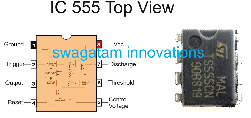
IC 555 Pinout Details
1) Circuit Diagram of a Simple Voltage Doubler using IC 555
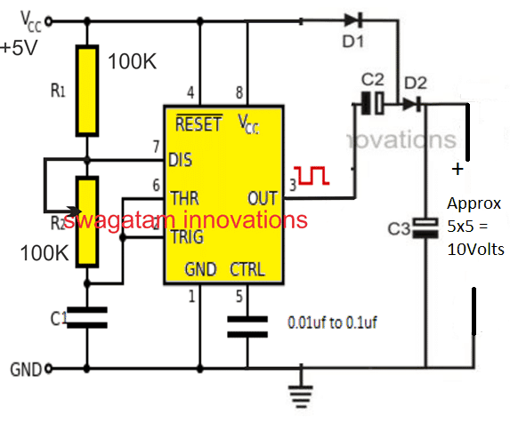
Referring to the above example, we can see an IC 555 circuit configured as an astable multivibrator stage, which is actually a form of oscillator, and is designed to produce a pulsating DC (ON/OFF) at its output pin#3.
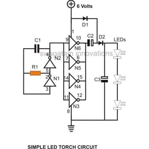
If you recall, we had discussed an LED torch circuit in this website, which quite identically uses a voltage doubler circuit, albeit the oscillator section is created using an IC 4049 gates.
Basically, you can replace the IC 555 stage with any other oscillator circuit and still get the voltage doubling effect.
However using IC 555 has a slight benefit since this IC is able to generate more current than any other IC based oscillator circuit without using any external current amplifier stage.
How the Voltage Doubler Stage Operates
As can be seen in the above diagram, the actual voltage multiplication is implemented by the D1, D2, C2, C3 stage, which are configured as a half-bridge 2-stage voltage multiplier network.
Simulating this stage in response to the IC 555's pin#3 situation can be a little difficult, and I am still struggling to get it running in my brain correctly.
As per my mind simulation, the working of the mentioned voltage doubler stage can be explained as given in the following points:
- When the IC output pin#3 is in its low logic or ground level, D1 is able to charge C2, since it is able to get forward biased through C2 and pin#3's negative potential, also simultaneously C3 is charged via D1, and D2.
- Now, in the next instant as soon as pin#3 becomes at high logic or at the positive supply potential, things get slightly confusing.
- Here C2 is unable to discharge via D1, so we have a supply level output from D1, from C2, and from C3 also.
- Many of the other online sites say that at this point the stored voltage inside C2, and the positive from D1 is supposed to combine with the output of C3 to produce a doubled voltage, however that does not make sense.
- Because, when voltages combine in parallel, the net voltage does not increase. The voltages must combine in series to cause the desired boosting or the doubling effect.
- The only logical explanation that can be derived is, when pin#3 becomes high, C2's negative being at the positive level and its positive end also held at the supply level, it is forced to produce a reverse charge pulse which adds up with the C3 charge, causing a instantaneous potential spike having a peak voltage twice that of the supply level.
If you have a better or technically more correctexplanation, please do feel fre to explain it through your comments.
How much Current?
Pin#3 of the IC is assigned to deliver a maximum of 200mA current, therefore the maximum peak current can be expected to be at this 200mA level, however the peaks will get narrower depending on the C2, C3 values.
Higher value capacitors might enable fuller current transfer across the output, therefore make sure the C2, C3 values are optimally selected, around 100uF/25V will be just enough
A Practical Application
Although a voltage doubler circuit can be useful for many electronic circuit applications, a hobby based application could be to illuminate a high voltage LED from a low voltage source, as shown below:
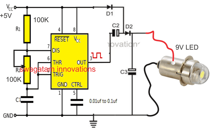
In the above circuit diagram we can see how the circuit is used for illuminating a 9V LED bulb from a 5V supply source, which would normally be impossible if the 5V was directly applied on the LED.
Relation between Frequency, PWM and the Voltage Output Level
The frequency in any voltage doubler circuit is not crucial, however faster frequency will help you to get better results than slower frequencies.
Similarly for the PWM range, the duty cycle should be roughly 50%, narrower pulses will cause lower current at the output, whereas too wide pulses will not allow the relevant capacitors to discharge optimally, again resulting in an ineffective output power.
In the discussed IC 555 astable circuit, the R1 can be anywhere between 10K and 100K, this resistor along with the C1 decides the frequency. C1 consequently can be anywhere between 50nF to 0.5uF.
R2 will fundamentally enable you to control the PWM, therefore this can be made into a variable resistor through a 100K pot.
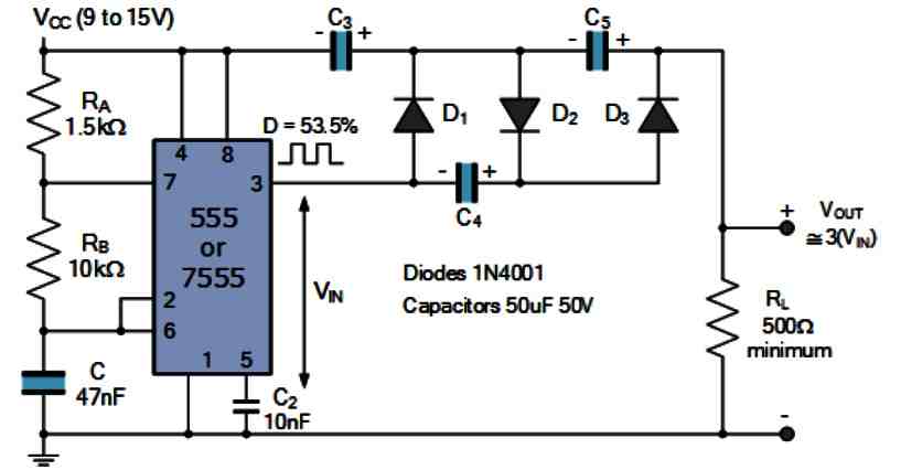
2) Another 555 Voltage Doubler
The second circuit shown below is another IC 555 based DC voltage-doubler, which produces a DC output voltage that is almost double the supply voltage.
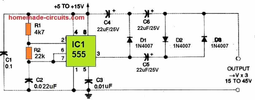
The output of the 555 is connected to a voltage-doubler circuitry consisting of capacitors C4 and C5, as well as diodes D1 and D2.
As long as the output is unloaded, the circuit provides an output that is about nearly twice the supply voltage. The exact value of the output is:
Vout = 2 x Vpeak (Vfd1 + Vfd2)
Where Vpeak represents the squarewave generator's peak output voltage, and Vfd1 and Vfd2 indicate the multiplier diodes D1 and D2's forward voltage drops (approximately 600 millivolts).
As soon as the circuit's output is loaded, the output voltage drops. Any DC source between 5 and 15 volts might operate with the voltage doubler circuit shown above.
This can give voltage outputs across a range of roughly 10 to 30 volts due to its voltage doubling effect. Applying additional multiplier stages to the circuit will result in a higher voltage.
3) Voltage Doubler Using IC 4049 NOT gates
The following CMOS IC based circuit can be used for doubling any DC source voltage (up to 15 V DC).
The presented design will double any voltage between 4 to 15 V DC and will be able to operate loads at current not more then 30 mA.
As can be seen in the diagram, this DC voltage doubler circuit employs just a single IC 4049 for achieving the proposed result.
IC 4049 Pinouts
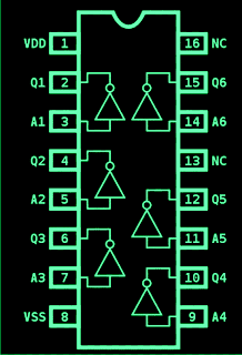
Circuit Operation
The IC 4049 has six gates in all which are all effectively for generating the discussed voltage doubling actions. Two of the gates out of the six are configured as an oscillator.
The extreme left of the diagram shows the oscillator section.
The 100 K resistor and the 0.01 capacitor form the basic frequency determining components.
A frequency is imperatively required if a voltage stepping actions needs to be implemented, therefore here too the involvement of an oscillator becomes necessary.
These oscillation become useful for initialing the charging and discharging a set of capacitors at the output which amounts to the multiplying of the voltage across the set of capacitors in a such a way that the result becomes twice the applied supply voltage.
However the voltage from the oscillator cannot be preferably applied directly to the capacitors, rather its done through a group of gates of the IC arranged in a parallel way.
These parallel gates together produce a good buffering to the applied frequency from the generator gates so that the resultant frequency is stronger with respect to current and does not falter with relatively higher loads at the outputs.
But still keeping the specifications of a CMOS IC in mind the output current handling capacity cannot be expected to be larger than 40 mA.
Higher loads than this will result in the deterioration of the voltage level toward the supply level.
The output capacitor values can be increased to 100uF for getting reasonably higher efficiency levels from the circuit.
With 12 volts as the supply input to the IC, an output of around 22 volts may be acquired from this IC 4049 based voltage doubler circuit.
Parts List
- R1 = 68K,
- C1 = 680pF,
- C2, C3 = 100 uF/ 25V,
- D1, D2 =1N4148,
- N1, N2, N3, N4 = IC 4049,
- LEDs White = 3 nos.
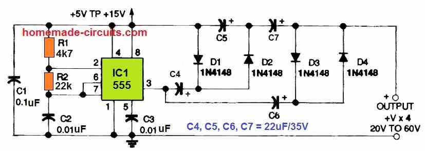
4) Voltage Tripler Circuit
The DC voltage quadrupler circuit shown in the next Figure, can be used to generate output voltages ranging from 20 to 60 volts.
5) Negative Voltage Doubler Circuit
The 5th circuit layout for a DC negative-voltage generator is shown in the following figure, which may produce an output voltage that is about similar in amplitude (double), but with a negative polarity.
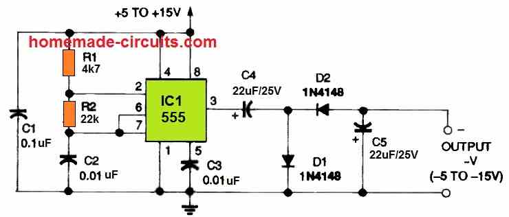
It likewise runs at 3 Hz and powers an output stage that includes capacitors C4 and C5, as well as diodes D1 and D2. The dual output of this circuit can be used to power ICs that need both positive and negative power from a single polarity supply.
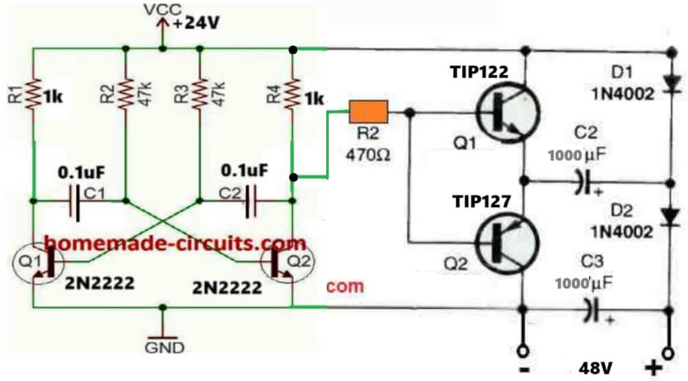
6) IC 555 Voltage Doubler Circuit with High Current Output
This sixth high current voltage doubler circuit presents a practical approach to generating a 24 V output from a 12 V battery. It utilizes the 555 timer in astable mode to generate a square wave signal at approximately 1 kHz. Here's how it works:
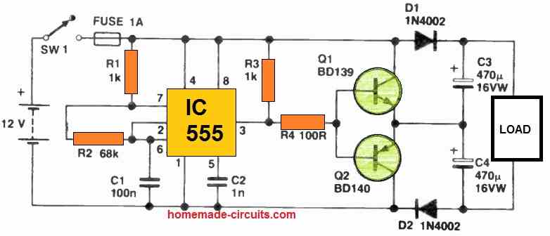
- The 555 timer is configured such that when pin 3 goes high, transistor Q1 becomes conductive, allowing the charging of capacitor C4 to nearly 12 V. Diode D1 prevents the discharge of capacitor C3 during this phase.
- Conversely, when pin 3 goes low, transistor Q2 conducts, enabling the charging of capacitor C3 in a similar manner, while diode D2 prevents the discharge of capacitor C4.
- The combined voltage across capacitors C3 and C4 results in the desired 24 V output.
Under no-load conditions, the output voltage measures approximately 24 V, but it decreases to about 20 V when a load drawing high current of 500 mA is connected.
It's important to note that heat sinks should be applied to the transistors to manage any heat generated during operation due to high current.
The current can be further increased by replacing the transistors with TIP122 and TIP127.
7) 12V to 24V Voltage Doubler Circuit using IC 4093
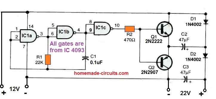
This 7th practical small circuit has an output current capability of 10 to 20 mA and may boost your working voltage by up to 175%.
A squarewave oscillator circuit has been configured using the gates IC1a and IC1b of a CD4093 dual-input NAND Schmitt-trigger CMOS IC.
The gate IC1c is rigged as a buffer for the output. The buffered output from IC1 powers Q1 and Q2 complementary transistors.
The voltage-doubler circuit, which is made up of D1, D2, C2, and C3, is driven by the square wave output at the transistor emitters to provide a boosted output.
The boost circuit will produce 24 volts at around 10 mA with a 12 volt supply, and roughly 18.5 volts at about 20 mA.
Make sure to connect the inputs of the spare unused gate to the ground line of the circuit.

Comments (57)
Thanks for the article. Converters are really useful especially when designing op-amp projects requiring dual supply voltage and you don’t have one at hand. I am currently working with 4558 and one of the requirements for this project is dual/split voltage, this article has been of great help to me.
Thanks
Thanks for your kind words and your candid feedback… I am glad you found the above circuits helpful…please keep up the good work…
If the capacitors are 63V or 80V, how much voltage can be input without burning anything out?
If we add an LM317T on the input side and <40V is input, what value of resistor on the LM317T would then guarantee no damage to components? (If you like, you can fix the duplicate Q1 & Q2 and post it.)
Is there an efficient way to cut off power to the inlet if the inlet has <400V and C3 reaches 48V?
You can use a software to calculate the LM317 voltage output. The 1000uF capacitors can be rated at 100V in that case.
To control 400V you can use a buck converter circuit.
What’s best for cheaply doubling 24V to almost 48V?
For low current DC, the above methods are the cheapest!
Which won’t burn out components if supplied with 24V to double? Will the sixth high current voltage doubler tolerate and double the 24V? (500mA or more sounds great!)
No, that circuit will not work with 24V.
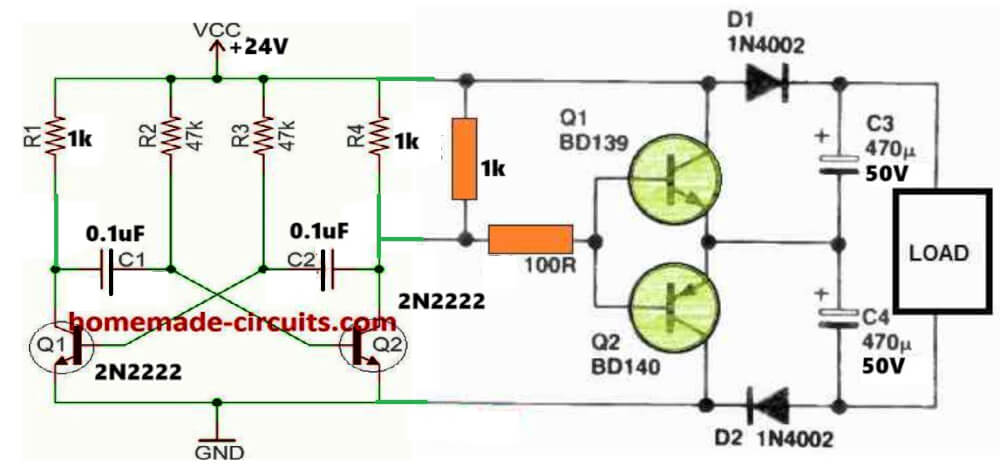
Instead you can try the following one:
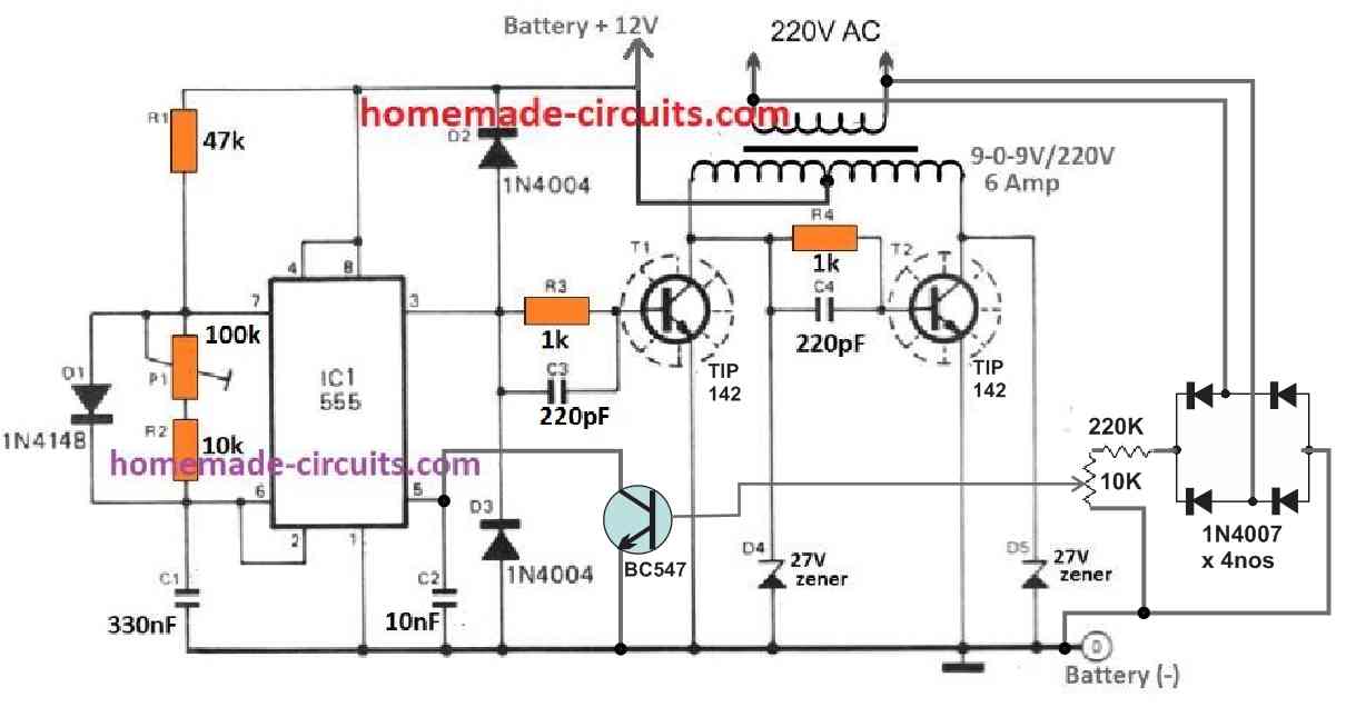
Thanks, but can it have a common ground on the input and output? (I need that.) Also, are there 3 of the 1k resistors, and is there a junction without a dot?
I have modified the last diagram as per your specifications:
All the black dots are connected, only the transistor bases crossing each other are not connected, rest all are connected.
Thanks!
How many watts do the resistors need to be?
What should I look for in 1000-microfarad capacitors to ensure a long life while the circuit is at low load?
Whenever it is not specified, you can assume them to be all 1/4 watt 5% CFR.
1000uF can be any standard electrolytic capacitor.
What about R2?
It is also 1/4 watt, actually by mistake I have shown two R2s, both are 1/4 watt, so all are 1/4 watt 5% CFR
I had gone through all the comments under that article, but there was not a single mention about such mistake of drawing those diodes in wrong direction. Anyway, do you think just by reversing the direction of those diodes, the ckt will start functioning normally? Please advise!!
Maddy, The diode direction does affect depending on where it is connected, whether it is connected to the positive or the negative side of the supply rail.
The second diagram which i suggested is taken from a reliable source, so you can try it, if still your circuit does not work then the problem could in your circuit connections.
Sirji the output has marginally increased. But it is still below the input. Previously the output was nearly 7v then after removal it raised up to 11v. Additionally, I checked voltage after every capacitor and it remains around 10-11v.
What should I do next?
Thanx again!!
Maddy, please try the following circuit, and let me know how it performs:
Sirji Good noon!!
Ckt built! But giving just half of input supply! I used 12v, 1.8a adapter for input! All the components were of same values as in the diagram but I used a 100k trimmer instead of 10k for feedback ckt! I don’t think that should creat any problem! How should I verify the fault if there is any? Please help Sirji!
Waiting for your kind advise!
Thanx…
Hi Maddy, please remove the feedback link from the circuit, and check the output voltage without the feedback link and let me know…
Thanx Sirji!
It seems like all the caps in diode-capacitor network are electrolytic but what about the other ones surrounding IC 555, like 0.01uF and 0.1uF? Are they ceramic caps?
Thank you again Sirji for the prompt reply!
Thanks Maddy,
Yes, the C1, C2, C3, can be ceramic disc type, no issues with that.
The remaining ones can be electrolytic.
Last few questions Sirji! 1st, can I use the same values as shown in the diagram? And 2nd, as per your advise, the feedback end should be taken to pin #5 of IC 555 but where should it begin? Please answer in reference to the quadrupler ckt!! Should I connect it directly after the diode-capacitor mesh and end it at pin #5 after removing the grounding capacitor already present there?
Thanx again!!
Yes, you can use the same values for the feedback as suggested in my previous example 555 inverter circuit.
The 220k resistor end must be connected to the +OUTPUT, and the 10k preset lower end to ground.
No need of the bridge rectifier.
The BC547 connects with the wiper arm of the preset, collector with the pin#5 of the IC 555, and emitter to the ground line…
No need to remove the existing capacitor at pin#5 of the IC.
Another question, how to include a feedback mechanism to give a constant voltage and current at the output!
Thanx!
Waiting for your kind advise!!
For the feedback, you can replicate the feedback mechanism as shown in the following 555 IC inverter design:
See how the feedback is taken from the 220V output through a 220k resistor, 10k preset and the BC547 transistor connected with the pin#5 of the IC 555.
Good evening Sirji, I was trying to make the voltage quadrupler ckt (4th ckt) from this article. But a few questions appeared after inspection! How to make it a variable output ckt? And the ckt claims to give four times the input voltage, that means nearly 60V, but all capacitors used there were rated for 35V. Do you think it is safe to use 35V caps for 60V output? Please advise!!
Thanx again!!
Thanks Maddy, for trying the quadrupler circuit.
For variable output you can add a feedback circuit configured with the pin#5 of the IC 555.
Yes, 35V is fine, since the quadrupler voltage is generated by the addition of the voltages across the capacitors.
Question I have a transformer that is 120v primary with two 12v secondaries, one of the secondaries has squared wire about 1/8th of an inch square. This transformer came out of a commercial 3500 to 4k inverter. (one of two transformers). The other secondary has a wire of about a 16 to 14awg. It is obvious that the bigger wires are the high current lines. The RMS voltage is about 17 to 19 volts. My question is will there be enough voltage to make a 13.8v high current power supply for transmitters? I have a schematic for a power supply that should work, my only issue is the RMS voltage.
I guess you are trying to find how much current output would be possible if 13.8V is derived from a RMS 19V source. That would depend on the wattage of the transformer. Wattage divided by the output voltage will give you the final accessible current. However if your power supply is a linear power supply then the excess voltage from the transformer will not be converted into current. You will need a buck converter for that!
I need a small and simple voltage doubling circuit and can’t find an existing one that meets my needs. On my 6v car, the battery/generator voltage may vary between 0 and 8v dc. I want to use a 12v voltmeter gauge to see my real-time voltage. The 12v gauge has a range from 8 to 16v. So, if I double my car voltage, I should be able to use a 12v gauge. I don’t expect to need much power consumption but I don’t know exactly how much the gauge requires.
Is there an existing simple solution you can imagine that I am not seeing?
Is there a simple circuit I can design and build myself?
You can simply use the following designs for getting the required 2X voltages from the car alternator. Remember the input must be AC and not DC. So a 6V AC from the generator, apply the input to any of the following set ups:
I am curious. I have a 12v 80a computer power supply that I would like to know if I take a sample of the 12v and use one of these circuits to double the voltage, and then drop it to 13.8v, if the current used would sustain the output of twenty-five or thirty amps without hurting the supply. These supplies are from server style computers. If you need pics of them email me and I will send them to you.
The above explained voltage doublers are for low current applications, in mA, so it cannot be used for high current applications. The power supply itself should have an internal adjustment to raise the output to the intended 13.8V
HELLO!
I am making voltage doubler circuit using IC CD4049 and i made exactly same circuit but i am unable to connect Vcc direct to inverter or pin 1 as you did in above circuit. and same with the Ground to pin 8. Can you please help me i m using multisim 12.0 .or tell me where can i merge VCC and GROUND.
Thank You.
Hi again,
I had already mentioned using the pwm output from a remote TX/RX combination and get a reverse mode.
the way they do it is with a rocker throttle at 2.5v in the neutral position forward uses 2.5 to 5V and reverse uses 25 to 0 volts. How would you suggest I extract the forward and reverse pwm signal an send it to my 0-5v esc? I also have to generate a signal to the reverse pin of the ESC when 2.5-0 volts is detected!
The voltage doubler circuit seems to fit the diagram you posted above. How would I go about extracting the 2.5 – 5V and 2.5-0 PWM signal?
I did an electronics course in the late seventies and haven’t touched it since!
Thanks in advance!
Pete
Hi, I do not know about what a rocket throttle is, however today any digital signal can be reversed either with a BJT stage or a NOT gate stage, for example if you connect a NOT gate at the output of the RX, the NOT gate will turn it upside down, meaning it will invert the input data at its output. So the 0V will become 5V, and the 5V will become 0V.
You can convert 2.5V to 5V, or 2.5 V to 0V with an op amp circuit, provided the actual operating power supply to the op amp is 5V
I think I’ll need to do it with an arduino! So I might as well build the esc as well! Probably easier to start from scratch instead of trying to fit different bit from here and there!
Thanks for the rapid reply!
Pete
P.S. it’s a rocker throttle not rocket. Push up with your thumb for forward pull it back for reverse!
OK thanks, wish you all the best!
That’s reverse uses 2.5-0 volts!
Pete
4093 cited at start of first paragraph under “Circuit Operation” must be a typo – that is a quad 2-input Schmitt Trigger NAND, not a hex inverter (NOT gate).
It is also worth mentioning that the 74xx14 (such as 74LS14, or 74HC14, etc) are suitable, but have a lower maximum supply voltage (typically 5.5 to 6.0V or so), while the 4049 (which you specify) can run to 18Vin. Thus, while they provide the same function as the 4049, if you’re hoping to run from a higher Vin (such as an automotive battery), the 4049 is preferred. The inverse is true as well – some 74xx series would be more appropriate for running from lower Vin.
Thank you for notifying the fault. Actually IC 4093 is a typo, it should be IC 4049, I’l correct it soon.
IC 4049 has a larger range since it’s a CMOS version, and therefore it becomes more suitable for these applications. It’s also less vulnerable to voltage fluctuations than 74XX14 versions.
IC 4093 can be also used as a voltage doubler. One of the gates could be configured as an an oscillator with R1/C1, while the remaining 3 gates could be used as buffer wit the output diode capacitor network for the required voltage doubling.
I need to convert the output from a single AAA battery or two in series to provide a positive voltage of not less then 3 volts with a power requirement of a maximum 50ma with as few parts as possible because of space restrictions.
If you are using two in series that would readily give you the required 3V. If you intend to use a single 1.5V cell, then you can try the following concept:
https://www.homemade-circuits.com/1-watt-led-driver-using-joule-thief/
hello sir the circuit works but now how can i modify it to power a 30watt load thanks
Olupot, this circuit cannot be used for high watt application, you can try the following concept instead
https://www.homemade-circuits.com/2013/03/simple-dc-to-dc-high-current-voltage.html
can u please state the diode spec its not proper i need to build this circuit
you can also refer to this article
https://www.homemade-circuits.com/2011/12/how-to-build-simple-hi-efficiency-led.html
thank you i was really inneed of this doubler
diodes are 1N4148, or 1N4007 will also do….
sir, we have research study now, and its all about 12 volts dc to 24 volts dc voltage multiplier. and our teacher ask how to calculate from 12 volts to 24 volts dc theoretical solution.
she want to have solution.
we give here a formula which Vout=2 x Vin., and she said wrong…
sir is there any solution for that?
thankx sir…
just for you Swagatam : tell teacher is like getting boob job,double to start out with then fall down as it age
For a boost converter or a transformer voltage doubler the formula could be
V(in) x I(in) = V(out) x I(out)
microfarad will need to be first converted to Farads for getting correct results
hello sir how are you
pls tell me sir how to calculate resistance and capacitance value for ic is there any formula
i found one in led chaser f= 1/1.39xRxC f is frequency is this correct whats 1.39 here sir pls tell me sir how to do it
Hello Puneet, the C will need to be in Farads, did you convert it in farads first??