In this post I have explained a 3 powerful yet simple 12V inverter circuits using a single IC SG 3525. The first circuit is equipped with a low battery detection and cut off feature, and an automatic output voltage regulation feature.
You may also want to read how to design a sine wave inverter from the scratch.
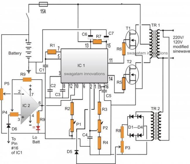
Design#1: Basic Modified Sine
In one of the earlier posts I discussed the pin out functioning of the IC 3525, using the data, I designed the following circuit which is though quite standard in its configuration, includes a low battery shut down feature and also an automatic output regulation enhancement.
The following explanation will walk us through the various stages of the circuit, I have explained them:
As can be witnessed in the given diagram, the IC SG3525 is rigged in its standard PWM generator/oscillator mode where the frequency of oscillation is determined by C1, R2 and P1.
Frequency Adjust
P1 can be adjusted for acquiring accurate frequencies as per the required specs of the application.
The range of P1 is from 100Hz to 500 kHz, here we are interested in the 100 Hz value which ultimately provides a 50Hz across the two outputs at pin#11 and Pin#14.
The above two outputs oscillate alternately in a push pull manner (totem pole), driving the connected mosfets into saturation at the fixed frequency - 50 Hz.
The mosfets in response, "push and Pull the battery voltage/current across the two winding of the transformer which in turn generates the required mains AC at the output winding of the transformer.
RMS Adjust
The peak voltage generated at the output would be anywhere around 300 Volts which must adjusted to around 220V RMS using a good quality RMS meter and by adjusting P2.
P2 actually adjusts the width of the pulses at pin#11/#14, which helps to provide the required RMS at the output.
This feature facilitates a PWM controlled modified sine waveform at the output.
Automatic Output Voltage Regulation Feature
Since the IC facilitates a PWM control pin-out this pin-out can be exploited for enabling an automatic output regulation of the system.
Pin#1 is the sensing input of the internal built in error Opamp, normally the voltage at this pin (non inv.) should not increase above the 5.1V mark by default, because the inv pin#1 is fixed at 5.1V reference internally.
As long as pin#1 is within the specified voltage limit, the PWM correction feature stays inactive, however the moment the voltage at pin#1 tends to rise above 5.1V the output pulses are subsequently narrowed down in an attempt to correct and balance the output voltage accordingly.
A small sensing transformer TR2 is used here for acquiring a sample voltage of the output, this voltage is appropriately rectified and fed to pin#1 of the IC1.
P3 is set such that the fed voltage stays well below the 5.1V limit when the output voltage RMS is around 220V. This sets up the auto regulation feature of the circuit.
Now if due to any reason the output voltage tends to rise above the set value, the PWM correction feature activates and the voltage gets reduced.
Ideally P3 should be set such that the output voltage RMS is fixed at 250V.
So if the above voltage drops below 250V, the PWM correction will try to pull it upward, and vice versa, this will help to acquire a two way regulation of the output,
A careful investigation will show that the inclusion of R3, R4, P2 are meaningless, these may be removed from the circuit. P3 may be solely used for getting the intended PWM control at the output.
Low Battery Cut-off Feature
Audio/Video Representation
The other handy feature of this circuit is the low battery cut off ability.
Again this introduction becomes possible due to the in built shut down feature of the IC SG3525.
Pin#10 of the IC will respond to a positive signal and will shut down the output until the signal is inhibited.
A 741 opamp here functions as the low voltage detector.
P5 should be set such that the output of 741 remains at logic low as long as the battery voltage is above the low voltage threshold, this may be 11.5V. 11V or 10.5 as preferred by the user, ideally it shouldn't be less than 11V.
Once this is set, if the battery voltage tends to go below the low voltage mark, the output of the IC instantly becomes high, activating the shut down feature of IC1, inhibiting any further loss of battery voltage.
The feedback resistor R9 and P4 makes sure the position stays latched even if the battery voltage tends to rise back to some higher levels after the shut down operation is activated.
Parts List
All resistors are 1/4 watt 1% MFR. unless otherwise stated.
- R1, R7 = 22 Ohms
- R2, R4, R8, R10 = 1K
- R3 = 4K7
- R5, R6 = 100 Ohms
- R9 = 100K
- C1 = 0.1uF/50V MKT
- C2, C3, C4, C5 = 100nF
- C6, C7 = 4.7uF/25V
- P1 = 330K preset
- P2---P5 = 10K presets
- T1, T2 = IRF540N
- D1----D6 = 1N4007
- IC1 = SG 3525
- IC2 = LM741
- TR1 = 8-0-8V.....current as per requirement
- TR2 = 0-9V/100mA Battery = 12V/25 to 100 AH
The low battery opamp stage in the above shown schematic could be modified for a better response as given in the following diagram:
Please use this online calculator to calculate the SG3525 parameters.
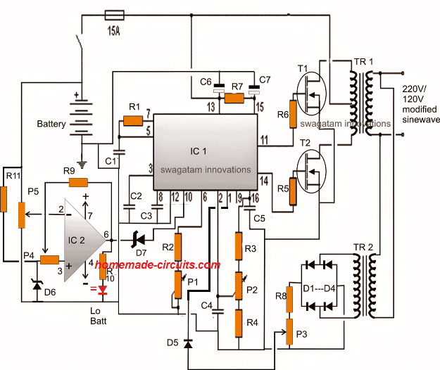
Here we can see that pin3 of the opamp now has it's own reference network using D6 and R11, and does not depend on the reference voltage from the IC 3525 pin16.
Pin6 of the opamp employs a zener diode in order to stop any leakages that might disturb pin10 of the SG3525 during its normal operations.
R11 = 10K
D6, D7 = zener diodes, 3.3V, 1/2 watt
Another Design with Automatic Output Feedback Correction
Circuit Design#2:
In the above section I have explained the basic version of IC SG3525 designed to produce a modified sine wave output when used in an inverter topology, and this basic design cannot be enhanced to produce a pure sine wave waveform in its typical format.
Although the modified squarewave or sine wave output could be OK with its RMS property and reasonably suitable for powering most electronic equipment, it can never match the quality of a pure sine wave inverter output.
Here I have explained a simple method which could be used for enhancing any standard SG3525 inverter circuit into a pure sine wave counterpart.
For the proposed enhancement the basic SG3525 inverter could be any standard SG3525 inverter design configured to produce an modified PWM output. This section is not crucial and any preferred variant could be selected (you can find plenty online with minor differences).
I have discussed a comprehensive article regarding how to convert a square wave inverter to a sine wave inverter in one of my earlier posts, here we apply the same principle for the upgrade.
Conclusion
That concludes our explanation on SG3525 based inverter circuit with low battery cut-off feature, frequency, PWM, and over voltage control features. If you have any questions or doubts please comment below to get quick replies from me.


Comments
Hi Swagatam;
I need pure sine wave inverter. I can use either any driver IC or PIC C IC. Which circuit do you advise? And which one is better, SCR or mosfet?
Hi Suat, i would recommend Arduino, or Atmega, or even PIC based designs, with MOSFETs.
kindly assist me with the Gerber file of this circle?
Thanks.
Sorry Offor, Gerber file is not available for this project..