Now in our earlier talks we saw that the N-channel Enhancement-mode MOSFET or e-MOSFET works nicely when we supply it with positive input voltage, so this is very important to remember.
This type of MOSFET has very high input resistance, almost close to infinity, and because of that we can use it easily like a switch.
So this high resistance makes it possible that we connect the MOSFET with almost any logic gate or driver that can give positive output signal, and it will work without problem.
Why We Can Parallel MOSFETs
Now we also noted that since the input Gate resistance is so high, then we can connect many MOSFETs in parallel, and we will not face trouble.
When we do this, then we can get the current handling capacity that our project needs, so this looks very useful.
But since paralleling many MOSFETs allows us to handle high current or high voltage loads, then it also brings some problems.
It can become very costly and very impractical because you will need many devices and extra circuit board space, so it is not always good.
Why Power FET Was Made
To solve this issue, engineers developed Power Field Effect Transistors or Power FETs and these work like a more efficient solution for high power use.
Types Of Field Effect Transistors
Now we must also understand that there are mainly two differences in field effect transistors. One is depletion-mode which is only for JFETs. The other is that MOSFETs can work both in enhancement-mode and depletion-mode.
But in this tutorial we will only focus on using Enhancement-mode MOSFET as a switch.
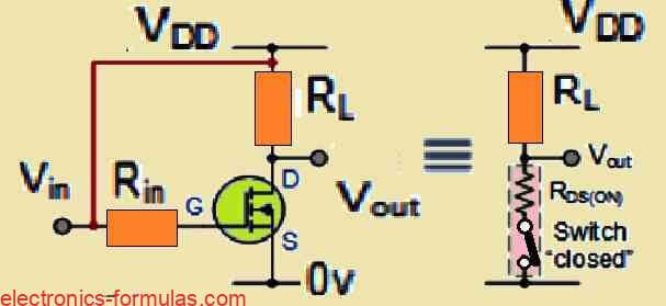
Using Enhancement-Mode MOSFET As Switch
These MOSFETs need positive Gate voltage to turn “ON”. And they need zero voltage to turn “OFF”.
So this behavior makes them very easy to use as switch, and we can connect them with logic gates without difficulty.
The working of Enhancement-mode MOSFET or e-MOSFET can be understood better from its I-V characteristic curves, which are shown below.
When VIN Is Zero
Now let us see what happens. When the input voltage VIN on the Gate of MOSFET is zero, then the MOSFET will allow almost no current to flow.
So in this case, the output voltage VOUT becomes equal to the supply voltage VDD.
This shows us that the MOSFET is in “OFF” state, and this state is called the “cut-off” region.
Characteristics Curves of a MOSFET

Now let us talk about the minimum ON-state gate voltage that we need so that we can keep our MOSFET in the ON position while it is handling a certain drain current. We can find this by looking at those V-I transfer curves which we already saw above.
What Happens When VIN Is HIGH
So when our input voltage VIN is increased to HIGH or it matches VDD, then the operating point of MOSFET, which we call Q-point, shifts to point A along that load line which we have drawn.
Now at this moment, the drain current ID starts to increase to maximum value, and this happens because the channel resistance is dropping down a lot.
Once we reach this proper point, then ID becomes constant value which does not really change with VDD but it depends only on gate-source voltage VGS.
So in this state, transistor works just like closed switch. But we need to note that the channel ON-resistance does not fully vanish. It becomes very small but it never becomes zero because of that RDS(on) value.
What Happens When VIN Is LOW
Now when VIN is LOW or it becomes zero then our MOSFET Q-point moves from point A to point B along the same load line.
In this case, the channel resistance goes very high, so transistor behaves like open circuit, and that means no current can pass through the channel.
How It Works As Switch
So if we keep changing or toggling the gate voltage of MOSFET between HIGH and LOW, then it starts acting like single-pole single-throw (SPST) solid state switch. This continuous action of ON and OFF is what we understand as switching operation.
Cut-Off Region
Now let us see about cut-off region. In this region, the condition for transistor operation is such that we have zero input gate voltage VIN, zero drain current ID and output voltage VDS is equal to VDD.
This means that for enhancement type MOSFET, the conductive channel is completely closed so the device is switched OFF.
Characteristics of the Cut-off Region

- The input and gate are grounded at 0 volts.
- The gate-source voltage is less than the threshold voltage, which means VGS is less than VTH.
- The MOSFET is in the “OFF” state, which we refer to as the cut-off region.
- There is no drain current flowing through, so ID equals 0 amps.
- The output voltage, VOUT, is equal to VDS, which equals VDD, and we can say it is “1.”
- In this situation, the MOSFET operates like an “open switch.”
Now therefore when we work with an enhancement-mode MOSFET as a switch, then we may choose the cut-off zone or we may say "OFF mode". Let us see what this means step by step.
This OFF mode has been characterized by the fact that ID equals 0, since the gate voltage is lower than the threshold voltage, that is VGS < VTH. So we understand that no current flows.
Now a P-channel enhancement MOSFET requires a gate voltage that is more positive with respect to the source, so you must remember this condition.
Saturation Region
Now let us talk about the saturation region, which we also call the linear region of a transistor.
In this case, we have its biasing set up in such a way that we are increasing the gate voltage to its maximum value, so let us understand what happens then.
This setup makes the channel resistance which we call RDS(on), very low, so this allows the maximum drain current to flow through our MOSFET switch.
So for enhancement-type MOSFETs, this means that the conductive channel is now wide open and we can say that the device is switched ON.
Characteristics of the Saturation Region
- Essentially our MOSFET acts like a low-resistance “closed switch,” making it super efficient.
- We connect the input and gate to VDD.
- The gate-source voltage is way higher than the threshold voltage, so VGS is greater than VTH.
- This means our MOSFET is fully “ON” and operating in that saturation region.
- We can expect the maximum drain current to flow, which we can calculate as ID = VDD / RL.
- In an ideal scenario, VDS would be 0V, indicating perfect saturation.
- The minimum channel resistance RDS(on) is less than 0.1Ω, which is pretty impressive.
- As a result of RDS(on), we see that VOUT is approximately 0.2V.
Now let us talk about what we mean by saturation region and ON mode when we use e-MOSFET as a switch, and we must see step by step.
How This Mode Starts
So basically this mode happens when the gate-source voltage VGS becomes higher than the threshold voltage VTH, then we can say the MOSFET is entering ON mode.
When this happens then the drain current ID reaches its highest value, so now the MOSFET is fully conducting.
For P-Channel MOSFET
Now if we are working with P-channel enhancement MOSFET, then we must remember that the gate potential has to be lower than the source, otherwise it will not switch properly.
Controlling RDS(on)
When we apply correct drive voltage to the gate of the FET, then something very important happens. We can control the resistance between drain and source, and this resistance is called RDS(on).
This RDS(on) can change between very high OFF resistance of hundreds of kΩ, which works like open circuit, and very low ON resistance of less than 1Ω, which works like short circuit.
Why It Is A Good Switch
So now when we use MOSFET like switch, we get very big advantage. We can turn it ON very fast or we can also make it turn ON in slow way, so we have choice.
Also we can decide if it has to allow high current or low current, so it gives us control.
Since it can turn ON and OFF very efficiently, so it becomes excellent choice for switch.
Actually it can change its state much faster than standard bipolar junction transistors, so that is why MOSFET is selected for switching jobs.
Analyzing a MOSFET as a Switch Example

Now let us talk about the gate input voltage that we apply to MOSFET and we call this VGS. We adjust this voltage to some positive level and that activates the device, so the lamp load turns ON when VGS is positive. But when VGS is zero voltage level, which is 0V, then the lamp load turns OFF.
Using Inductive Load With MOSFET
Now let us say we remove the resistive lamp load, and we put inductive load like coils, solenoids, or relays. Then we must add one flywheel diode in parallel with that inductive load.
This diode is very important because it protects the MOSFET from back electromotive force, which we call back-emf and that is generated by the inductive load.
Switching Resistive Load
So what we see here is very simple circuit, and it is for switching resistive load like lamp or LED. But since we are using power MOSFETs, then if we want to switch inductive or capacitive loads, it becomes very important to add protection. This is needed so that the MOSFET does not get damaged.
Inductive Load Vs Capacitive Load
Now it is interesting that driving inductive load is very different compared to driving capacitive load. For example, let us take capacitor which has no charge. Then it will behave like short circuit and this will cause very big inrush current.
But on the other side when we cut off voltage from inductive load, then we will see large reverse voltage buildup, and that happens because magnetic field collapses. This situation generates induced back-emf in the inductor winding and that can be very dangerous for the MOSFET.
Summary
So we can now summarize switching characteristics of both N-channel and P-channel MOSFET in table form.
| MOSFET Type | VGS ≪ 0 | VGS = 0 | VGS ≫ 0 |
| N-channel Enhancement | OFF | OFF | ON |
| N-channel Depletion | OFF | ON | ON |
| P-channel Enhancement | ON | OFF | OFF |
| P-channel Depletion | ON | ON | OFF |
Now let us see one important difference between N-channel MOSFET and P-channel MOSFET. For N-channel MOSFET, we need to make sure that the gate terminal is more positive than the source. So when gate is more positive, then electrons get attracted, and then current starts to flow through the channel.
But when we use P-channel MOSFET, then situation is different. Here conduction happens because of movement of holes and not electrons.
So for P-channel MOSFET to work properly, we must make gate terminal more negative than source. Since this is the rule, then device will stop conduction only when gate voltage goes above source voltage and becomes more positive. At that time it will enter cut-off state.
Using Enhancement-Type Power MOSFET As Switching Device
Now let us say we want to use enhancement-type power MOSFET like analog switching device, then we must control it carefully.
We need to move it only between two main regions. First region is Cut-off Region, where VGS is equal to 0V or VGS is negative. Second region is Saturation Region, where VGS(on) is positive.
So we must always shift it between these two states when we use it as switch.
Power Dissipation In MOSFET
Now let us see about power dissipation PD inside MOSFET. It depends on few factors. Main factor is the current flowing through channel ID when device is in saturation. Another factor is ON-resistance of the channel, which we call RDS(on).
So when current ID flows and we have some RDS(on), then power gets dissipated in form of heat.
Practical Example
Now let us take simple example. Suppose we have current flowing through P-channel MOSFET when it is in saturation region. Then we can calculate how much power is wasted by using ID and RDS(on).
So we must know this relation if we want to use MOSFET properly in circuit without heating problem.
Solving a MOSFET Switch Circuit Problem #1
Let's imagine we have a lamp that is rated at 12 volts and 25 watts, and it is operating at full capacity. We also have a standard MOSFET with a channel on-resistance (RDS(on)) of 0.12 ohms. We want to calculate the power that is dissipated in the MOSFET switching device under these conditions.
We will first calculate the current passing through the lamp using the following fomula:
P = V * ID
∴ ID = P/V = 25/12 = 2.08 Amps
Next, we will calculate the power dissipated in the MOSFET, in the following manner:
P = I2 * R
PD = I2D * RDS
∴ PD = 2.08 * 0.12 = 0.25 watts
Understanding RDS(on) of a MOSFET
Now let us think about how we use MOSFET to control DC motors or high inrush current loads, and we at once see that the "ON" state resistance RDS(on) across drain and source is very important.
So you may ask yourself then, why this parameter is so crucial.
Why RDS(on) Is Important
Now this parameter is very important because when we use MOSFET to control DC motors, then we find that the motor takes a big surge of current as soon as the motor starts to rotate.
This sudden increase comes because the initial current of motor is restricted only by very low resistance of its winding, so current shoots up.
Let us look at this by the basic power formula P = I²R.
So if the RDS(on) value is high, then a big amount of power is wasted inside MOSFET, and this wasted power turns into heat.
So now if it is not handled properly, then temperature rises a lot, and this can make MOSFET overheat and get damaged.
But if the MOSFET has low RDS(on), then it becomes a very good quality because it helps to reduce the saturation voltage VDS(sat) = ID × RDS(on), and so the MOSFET works at lower temperature.
Actually power MOSFETs usually have RDS(on) value less than 0.01 ohms.
So having such small resistance helps MOSFET to stay cool and that increases life and reliability of the device in many uses.
Maximum Drain Current Limit
When we think about MOSFET as a switching device, one of the first limits we must think about is maximum drain current that it can handle safely.
This limit is very critical, since RDS(on) is main measure of MOSFET efficiency. In simple words, it shows ratio of VDS to ID during the time MOSFET stays in ON state.
So when we use MOSFET or other field effect transistor as switch, it is always best to choose device with low RDS(on).
But if we do not have such type, then we should put the MOSFET on big enough heatsink, so that heat can go out safely.
This method is very important because it reduces the danger of thermal runaway and damage.
MOSFET Versus BJT For High Current
Although power MOSFETs made for switching already have surge current safety, but since high current applications demand more, then sometimes a bipolar junction transistor becomes better option.
Gate Resistance And Driving Feature
Now when we look at MOSFET more closely, one thing stands out clearly, and that is very high gate resistance.
This property, together with very fast switching speed and easy driving, makes MOSFET ideal for use with op amps or logic gates.
But we must be very careful in deciding the correct gate source input voltage. Because when MOSFET is used as switch, it is very critical that the RDS(on) is low enough depending on input gate voltage.
Gate Threshold Consideration
It is important to note that low threshold power MOSFETs may not turn ON until minimum 3V or 4V is applied at gate.
So if logic gate output gives only +5V, then it may not be enough to fully saturate the MOSFET.
But thankfully we have MOSFETs designed with lower threshold between 1.5V to 2.0V, so they can work well with TTL and CMOS logic gates.
MOSFET In Motor Control
Moreover power MOSFETs are very useful to control acceleration of DC motors or brushless stepper motors with computer logic or PWM control.
Since DC motor has strong starting torque that is directly proportional to armature current, then we can use MOSFET switching with PWM to get very efficient speed control.
This method makes motor run smooth and quiet, and also gives better performance and control in many applications.
Understanding the Working of a Simple MOSFET Motor Controller Circuit

Referring to the diagram above, when we are dealing with a motor load which is inductive, we need to connect a simple flywheel diode right across the inductive load.
This diode helps to get rid of any back emf that the motor generates when we turn the MOSFET “OFF.”
To make things even better, we can set up a clamping network by adding a zener diode in series with the flywheel diode. This setup allows for faster switching and gives us better control over the peak reverse voltage and how long it takes to drop out.
For some extra safety, we can also add another silicon or zener diode, which we can see as D1, across the channel of the MOSFET switch whenever we are working with inductive loads like motors, relays, or solenoids.
This extra diode helps to suppress those sneaky over-voltage switching transients and noise, giving our MOSFET switch some added protection if we need it.
And let us not forget about resistor RGS! This resistor acts as a pull-down resistor to help pull the TTL output voltage down to 0V when we switch the MOSFET “OFF.”
How to Configure a P-Channel MOSFET as a Switch

Up to this point, we have been examining the N-channel MOSFET employed as a switch, with the MOSFET situated between the load and the ground.
This configuration allows us to refer to the gate drive or switching signal as grounded, known as low-side switching. However in certain situations, we genuinely require a P-channel enhancement-mode MOSFET, with the load directly linked to ground.
In this scenario the MOSFET switch is connected between the load and the positive supply rail, a method referred to as high-side switching—similar to the approach used with PNP BJTs.
Currently, with a P-channel device, the drain current travels in the negative direction. So, to activate the transistor, we must apply a negative voltage between the gate and source.
We are able to achieve this since the P-channel MOSFET is kind of “inverted,” with its source terminal connected to the positive supply, which we call +VDD.
Thus when the switch is set to LOW, the MOSFET activates or turns “ON,” and when the switch is set to HIGH, it deactivates or turns “OFF.”
This inverted configuration of a P-channel enhancement-mode MOSFET switch enables us to connect it in series with an N-channel enhancement-mode MOSFET.
This integration forms a complementary or CMOS switching component that functions effectively with a dual power supply.
Understanding the Working of a Complementary MOSFET as a Switch Motor Controller

Looking at the above image, we configured two MOSFETs to create a bi-directional switch utilizing a dual power supply. In this setup, the motor is connected between the common drain point and the ground reference.
When the input signal is LOW, the P-channel MOSFET turns on due to its gate-source junction being negatively charged. This leads the motor to turn in one direction, and we are exclusively using the positive +VDD power supply line to power it.
At present, when we apply a HIGH signal, the P-channel device turns OFF, while at the same time, the N-channel device turns ON due to its gate-source junction being positively biased.
This inversion causes the motor to rotate in the opposite direction because the voltage at the motor's terminals has now been reversed; it is drawing its power from the negative -VDD power source.
In this setup we use the P-channel MOSFET to connect the positive supply to the motor when we want it to move forward (this is known as high-side switching).
On the other hand, we employ the N-channel MOSFET to connect the negative supply to the motor when we want it to rotate in reverse (this method is known as low-side switching).
You may find numerous ways to configure the two MOSFETs for different applications. Both the P-channel and the N-channel devices can indeed be managed by one gate drive IC, as observed in certain configurations.
However the key point is this, to avoid cross conduction, when both the MOSFETs conduct simultaneously across the two polarities of the dual supply, we require rapid switching devices.
This is crucial because we aim to ensure there is a slight time interval between one MOSFET switching “OFF” and the other MOSFET switching “ON.”
A possible resolution to this problem is to control the gates of each MOSFET independently. This approach allows us to establish a third option that efficiently places the motor in a "STOP" state when both MOSFETs are in the “OFF” position.
This slight delay between the conduction of the two MOSFETs is also known as the deadtime.
Table to Indicate the Switching Control of two Complementary MOSFETs
| MOSFET 1 | MOSFET 2 | Motor Function |
| OFF | OFF | Motor Stopped (OFF) |
| ON | OFF | Motor Rotates Forward |
| OFF | ON | Motor Rotates Reverse |
| ON | ON | NOT ALLOWED |
Just a quick heads-up: it is really important that we do not allow any other combinations of inputs to be active at the same time. If we do, then it could lead to a situation where the power supply gets shorted out. This happens because both MOSFETs, FET1 and FET2, could end up being switched “ON” at the same time. And trust me, that would result in a big problem, just think of it as a fuse blowing with a loud bang! So we need to be careful!
References:


Need Help? Please Leave a Comment! We value your input—Kindly keep it relevant to the above topic!