An FET Current Source is one special type of active circuit that is using a Field Effect Transistor for giving a steady and constant current into a circuit. We are doing this because sometimes we want that current should not change, it should remain fixed and stable.
Why We Need Constant Current
Now you may think why we want such constant current. So the answer is that constant current sources and also their opposite side that we call current sinks, are very easy methods that help us for making biasing circuits or for making voltage references that always keep same current value.
Example Of Current Levels
Let us take example. We can make current like 100 microamperes uA, or 1 milliampere mA, or even 20 milliamperes mA by only one FET and one resistor. So you see it becomes very simple with few parts.
Applications Of Constant Current Source
We are using constant current sources in many places. One place is capacitor charging circuits, where timing must be correct. Another place is rechargeable battery charging, where steady current is important. We also use this in linear LED circuits where we want all LEDs glowing in equal brightness.
Making Voltage References
Also we can make resistive voltage references by using constant current source. Because since we already know the resistance value, and then if the current through that resistance is always constant, then we can apply Ohm’s law very easily for finding the voltage drop across that resistance.
Important Points For Accuracy
So when we are building a constant current source, then we must see two important things. First we must use low transconductance FETs. These are special FETs good for this job. Second we must select precision resistors so that the current can be converted into very precise and stable voltage.
Using JFETs And MOSFETs
Field Effect Transistors that we call FETs are widely used for making current sources. We can use Junction-FET JFET or Metal-Oxide Semiconductor FET MOSFET for situations where low current is needed.
Basic JFET As Controlled Resistor
In very simple form we can use JFET like a voltage controlled resistor. That means a small voltage on its gate can control how much current will flow between drain and source channel. So by adjusting that small gate voltage we can manage current properly. That is why JFET is very good choice for making reliable constant current sources.
Adjusting Junction FET Bias
Now let us talk about bias. In our last discussion about Junction Field Effect Transistor JFET we saw many features. We found that it is depletion-mode device. For example N-channel JFET is called normally-ON device. That means it stays ON and passing current until then we apply a negative VGS to make it OFF.
In same way, we also saw that P-channel JFET is also depletion device and it is also normally-ON. But here we must apply strong positive gate voltage if then we want to make it OFF.
How to Bias an N-channel JFET
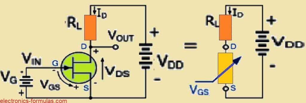
We see in the above diagram showing the usual way of arranging an N-channel JFET in a common source setup. We are mainly looking at how it is working in the active region.
Gate To Source Voltage
Now understand that the gate-source voltage VGS is nothing very different, it is simply the input voltage at the gate VG and that makes a reverse bias between gate and source. So this VGS is deciding how the channel is biased.
Drain To Source Flow
At the same time we also have VDS and current which are both coming from the supply VDD. This current is flowing from drain towards the source. We call this drain current by the label ID because it is the current through drain terminal.
Voltage And Current Relation
Right now we can think that the VDS is almost like the forward voltage drop of this JFET. This VDS is decided by how much ID is flowing at different levels of gate voltages VGS.
Maximum Drain Current
So when VDS is very low then the JFET channel is almost fully open, which means the gate is allowing full conduction. At this condition the ID becomes maximum and we call that maximum drain current as ID(sat) or many times just IDSS to make it short.
Pinch Off Condition
But when VDS becomes maximum then the JFET channel gets closed completely and we call this condition as pinch off. At pinch off the ID becomes almost zero and at this exact condition the VDS will become equal to VDD. The gate cut-off voltage VGS(off) is that specific voltage at which the channel stops conducting and becomes closed.
Common Source Biasing
Now when we arrange this type of common source biasing for an N-channel JFET then it basically fixes how the JFET will behave in steady condition when there is no input signal VIN. In this condition the VGS and ID remain at fixed values. We call this fixed steady condition as quiescent state.
Voltage Controlled Nature
Now here comes the important part. In a common source JFET we see that the gate-source voltage VGS is actually controlling how much current can move through the channel from drain to source. So this JFET is behaving like a voltage controlled device because the input voltage VGS is directly controlling the output current ID.
Output Characteristics
Because of this property we are able to create many output characteristic curves. We do this by plotting ID against VGS for a given JFET. These curves help us to study the working of the JFET in detail.
Output Characteristic of N-channel JFET

Using The JFET As A Constant Current Source
Now let us try to understand an n-channel JFET first. We know that this device is normally staying in the switched ON condition which means it will allow current to pass freely in normal state. But since the JFET behavior is different, then when we start making the gate-source voltage VGS more and more negative, then it begins to shut down itself and finally it can stop the current completely.
What is really happening inside is that the p-type depletion area which is surrounding the gate region is slowly getting bigger and bigger and then at one point that depletion grows so much that it completely blocks the conduction channel.
So for a p-channel JFET the same thing is happening but opposite, because in that case it is the n-type depletion regions which will do the blocking work.
So we can use this special property in a very useful way. When we adjust and set the gate-source voltage at some specific negative value, then we can actually decide and control how much current is allowed to flow through that JFET.
That means we can tune it to conduct any current from zero amps up to its maximum limit value IDSS. So that is the reason why we can use this device as a very good constant current source.
So now you can just look at the simple circuit given below that shows this working in the most clear way.
Zero-voltage Biasing of a JFET
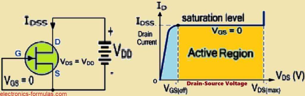
We see that the output characteristic curves of the JFET are showing a kind of relation between the drain current ID and the gate source voltage VGS, but here the drain source voltage VDS is kept constant. So we can say that you, me, or anybody who is checking these curves will notice this pattern clearly.
Now we also see that these curves are not changing so much even when we are making quite a big adjustment in the VDS value. That thing becomes very useful for us when we want to create or set a fixed operating point for the conductive channel inside the device.
Making A Simple Constant Current Source
So now let us talk about how we can make one of the very simple types of constant FET current source. What we do is that we short the gate terminal of the JFET with its source terminal. That is the method which is also shown in the diagram.
In this condition, the conductive channel of the JFET will stay open, and this allows the current which is flowing through it to be very near its maximum IDSS value. That happens because we are now keeping the JFET working in its saturated current region.
But we should not forget that even though this configuration of constant current is very simple, the overall performance is not really good. The JFET is forced to stay in full conduction mode and the IDSS current value is fully dependent on what exact type of JFET part we are using in the circuit.
Example Of Device Series
Like for example when we check the 2N36xx or the 2N43xx n-channel JFET series, then we see they are able to handle only a few mA current.
But when we check the bigger n-channel J1xx or PN4xxx series, then we see they are able to manage many tens of mA current. So it is important that we realize how the IDSS value, which means the zero gate voltage drain current, can keep changing a lot even inside devices which are having the same part number.
The manufacturers normally give these variations in their datasheet. In that datasheet you will see both the minimum value and the maximum value of the IDSS mentioned clearly.
FET As A Voltage Controlled Resistor
Another important thing which we must keep in our mind is that an FET is actually working like a resistor that is controlled by a voltage.
The conductive channel which is inside the FET has its own resistive value. That resistive path is in series between the drain and the source terminals. This resistance of the channel is called as RDS.
So when we see the condition that VGS is equal to zero, then the maximum current is able to pass from drain to source. That means in this condition the channel resistance RDS is staying at its lowest value, and this is absolutely true.
But you may think that this resistance is going to be zero, but it is not so simple like that. Actually this resistance is at some low ohmic level which is decided depending on how the JFET has been manufactured. This can sometimes be as high as almost 50 Ohms.
Now when we are explaining about the conduction of the FET, then we call this resistance as RDS(ON). This RDS(ON) becomes lowest when VGS is set to zero.
That also means if we are having a low IDSS, then we will find that the RDS(ON) will be high. But if we are having a high IDSS, then the RDS(ON) will be lower.
Biasing The JFET For Current Source
So now let us see how we can bias the JFET in such a way that it works like an FET current source. We can adjust this at any current level which is smaller than the saturation current value. The saturation current is IDSS that happens when VGS is equal to zero volts.
When the gate voltage is reaching the VGS(off) cut-off value, then the drain current ID is going to drop to zero. That happens because the conductive channel becomes closed fully.
So finally it is important for us to remember that the current will always keep flowing through the channels of the JFET device as long as the device is working inside its active region. This is exactly what we can see also in the characteristic diagrams.
Understanding the Transfer Curve of a JFET
In the case of a P-channel JFET, the VGS(off) threshold voltage will be a positive value along with the saturation current IDSS at VGS of zero volts will remain unchanged compared to an N-channel JFET.
Additionally we must look that the transfer curve is non-linear due to the fact that the drain current rises more rapidly as VGS gets closer to zero volts.
Understanding Negative-voltage Biasing of JFET
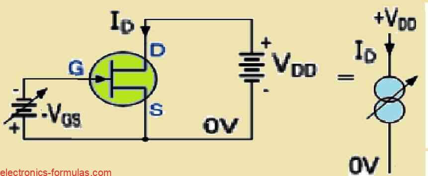
We must remember always that the JFET is basically a depletion mode type device, and that simply means it is normally staying in the condition which we call as always ON. So it will allow current flow naturally unless we stop it with some gate biasing.
Gate Voltage Requirement For N Channel And P Channel
Now you see, for the N-channel JFET we have to apply a negative gate voltage if we want to turn it OFF, but for the P-channel JFET we have to apply a positive gate voltage if we want to do the same OFF function. So both types act opposite regarding the gate voltage polarity.
Effect Of Wrong Bias
Now then if we make a mistake and we bias the N-channel JFET with a positive voltage or we bias the P-channel JFET with a negative voltage, then we are not turning it OFF but instead we are actually opening its conductive channel more strongly. That means the current through the channel which we call as ID will increase, and it can go beyond its safe maximum value which we call as IDSS.
Looking At The Characteristic Curves
So since that is dangerous, we must see the characteristic curves carefully where ID is plotted against VGS. Then we find that by applying some negative VGS voltage like -1V, -2V, or -3V, we can actually set the device into a mode where it becomes a fixed constant current source. That means JFET itself will pass a fixed current.
Current Control Possibility
So this way we can choose the current value which we want, anywhere between zero and IDSS. That gives us a nice flexibility because you and me can design circuits and set current as per requirement.
More Accurate Constant Current
But then when we want a more precise constant current source which also regulates in a better way, then it is a good idea to bias the JFET around 10 percent to 50 percent of the full IDSS value. That region is most stable.
Advantage Of This Approach
This kind of biasing does not only improve the accuracy but also reduces the I²R losses happening in the channel resistance. Since the losses are reduced then naturally the heating of the device also becomes less. So we get accuracy and less heat both together.
Setting The Operating Point
So at the end we can clearly see that by applying negative voltage to the gate of the N-channel JFET, or by applying positive voltage to the gate of the P-channel JFET, then we can fix the exact operating point of the device.
Drain Current Behavior
That operating point allows the channel to pass a specific drain current ID. Now for different values of VGS we can write down a mathematical expression for ID and that formula helps us to understand how the JFET will behave under different biasing conditions in real circuit.
Formula for Calculating the JFET Drain Current
ID ≅ IDSS [1 - (VGS/VGS(off))]2
Solving a FET Constant Current Source Problem #1
Looking at the manufacturer's datasheet for the J107 N-channel switching JFET, we can see that it has an IDSS value of 35 mA when the gate-source voltage (VGS) is equal to 0 volts. Additionally the datasheet specifies a maximum VGS(off) value of -6.0 volts. With these values in mind, let us calculate the drain current (ID) of the JFET for different gate-source voltage levels, specifically when VGS = 0 volts, -2 volts, and -5 volts.
With the VGS = 0V, we have the maximum drain current passing through the conductive channel, which is now full open.
So, ID = IDSS = 40 mA
In the condition when we have VGS = -2 V, then:
ID ≅ IDSS [1 - (VGS/VGS(off))]2
= 40[1 - (-2/-6)]2
= 0.04(1 - 0.333)2
= 0.04(0.444)
ID = 17.8 mA
In the situation when we have VGS = -5 V, then:
ID ≅ IDSS [1 - (VGS/VGS(off))]2
= 40[1 - (-5/-6)]2
= 0.04(1 - 0.833)2
= 0.04(0.0278)
ID = 1.1 mA
Transfer Characteristics Curve of JFET J107
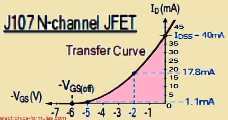
So we see it is clear that the drain current ID, decreases as the gate-source voltage VGS, approaches the gate-source cut-off value VGS(off).
Although we measured the drain current at two distinct locations in this simple instance, but a more accurate depiction of the curve might be obtained by using more VGS values ranging from zero to cut-off.
Using a JFET as a Current Source
So now we start thinking that when we use a JFET then we can make it actually work like one voltage controlled constant current source. We see that this thing happens then when we reverse bias that gate source junction of the device.
Since we talk about N channel type then we must apply some negative gate source voltage VGS, but when we use P channel type then we must apply some positive VGS. Now here comes the tricky part that we find, because the JFET will normally need two different voltage supplies, one supply is for that VDD and another separate supply is for that VGS.
But so now here is where the matter becomes more interesting for us. Let us imagine that we put one resistor right between that source pin and ground point which stays at 0 volts, then that simple act itself will create one self biasing arrangement for VGS.
Because of that arrangement, the JFET will start operating like one constant current source and we will need only that single VDD supply voltage. That means we can simplify the whole setup quite a lot and we will not require two separate supplies. So now let us carefully look at the circuit diagram below so that we can understand in practice how exactly this working is happening.

So now when we first take a look at this type of configuration, then we may feel like that it is almost same as JFET common drain circuit which is also called source-follower, and we remember that we already studied that in the JFET tutorial. But then our eyes catch some similarities here, and that makes us feel like both are related.
The main Difference
But since we watch it closely, then we find the main difference. Here even though the gate terminal of the FET is still tied directly to the ground which means VG is equal to zero, still the source terminal is not at zero volt but actually it is sitting above zero volts.
This strange thing is happening because of the voltage drop that develops across the external source resistor, and we call that resistor RS.
Why VGS Becomes Negative
So what this tells us is that when the channel current starts flowing through this external source resistor, then it automatically creates a condition where the gate-to-source voltage of the JFET becomes less than zero. In other words VGS is more negative than zero.
The Role Of Source Resistor RS
Now let us talk in detail about what this external source resistor RS is really doing here. That resistor is actually providing a feedback voltage, and that feedback acts in a way that it self-biases the gate terminal of the JFET.
This kind of clever arrangement makes sure that the drain current through the channel keeps moving steadily even if the drain-source voltage is trying to change. So basically to make the whole thing work, what we actually need is only the supply voltage VDD, because this same VDD is giving us the required drain current as well as the required biasing.
How The Biasing Works
So when we try to understand how the JFET is operating, then we see that the voltage drop across the source resistor, which we call VRS, is what decides the gate bias voltage VGS. And this VGS is what controls the channel current, exactly like we explained earlier.
Changing RS Value
Basically what we find is, if we increase the resistance value of RS, then the drain current ID in the channel will go down. But oppositely if we decrease the resistance value, then ID will rise higher.
So now when we are thinking about building a JFET constant current source circuit, then obviously we begin to wonder what value of RS will be the best to use for getting the correct current.
Finding RS Value From Data Sheet
To solve this we can take the manufacturers data sheet for that specific N-channel JFET. In that sheet we will find some important fixed values like VGS(off) and IDSS.
Once we know these two values, then we can take the JFET equation for the drain current ID and rearrange it in such a way that it tells us what the value of VGS should be for any chosen drain current ID which lies between zero and IDSS.
So this means that, with only a little help from the data sheet and with some easy calculations from our side, we can decide what resistor value RS should be and then we can design our JFET circuit in a way that it works like a constant current source, exactly like we want.
Formula for Calculating the JFET Gate to Source Voltage
ID ≅ IDSS [1 - (-VGS/-VGS(off))]2
∴ VGS = -VGS(off) [1 - √(ID/IDSS)]
Once the gate-to-source voltage needed for a specific drain current has been calculated, then we can use the Ohm's law (R = V/I) to get the necessary source biasing resistor value.
The following equation can be used to calculate JFET Source Resistor:
RDS = VGS/ID (Ω)
Solving an FET Constant Current Source Problem #2
Let us take a look at the J107 N-channel JFET device that we mentioned earlier. This particular device has an IDSS value of 40mA when VGS equals zero and it also has a maximum VGS(off) value of -6.0 volts. So we want to calculate the value of the external source resistor that we need in order to create a constant channel current of 20 mA.
After this we will repeat the calculation for a constant channel current of 5 mA. So we will be working with these two different current levels to see what resistor values we need to use in our circuit to achieve those specific constant channel currents.
Let's begin by solving the VGS for an ID = 20 mA
VGS = -VGS(off) [1 - √(ID/IDSS)]
VGS = -6 [1 - √(20/40)] = -6(1 - 0.707) = -1.75 Volts
∴ VGS = -1.75 V
Now, RDS = VGS/ID
= 1.75/20 = 1.75/0.02
= 87.5 Ω
Next, let's calculate VGS when ID = 5 mA
VGS = -VGS(off) [1 - √(ID/IDSS)]
VGS = -6 [1 - √(5/40)] = -6(1 - 0.353) = -1.75 Volts
∴ VGS = -3.90 V
Next, RDS = VGS/ID
= 3.90/5 = 3.90/0.005
= 780 Ω
So when we know both VGS(off) and IDSS, we can actually use the equations we talked about before to find out the source resistance that we need to bias the gate voltage for a specific drain current.
In our simple example we found that this resistance was 87.5 Ω when we wanted a drain current of 20 mA and it was 780 Ω when we aimed for a drain current of 5 mA.
This means that by adding an external source resistor we can easily adjust the output of our current source to get just the right amount of current flowing.
Now if we wanted to take this a step further, we could swap out those fixed value resistors for a potentiometer. This would allow us to make our JFET constant current source fully adjustable, which can be so useful!
For example instead of using two fixed source resistors like in our previous example we could just use one 1kΩ potentiometer or trimmer.
Not only does this give us the flexibility to adjust the current as needed but it also means that the drain current in our JFET constant current source circuit will stay constant even if we make changes in the VDS values.
Solving an FET Constant Current Source Problem #3
Here we want to use an N-channel JFET to control the brightness of a 5mm red LED load, and we want to be able to vary that brightness between 8 mA and 15 mA.
To make this happen, we are going to set up a JFET constant current source circuit that will be powered by a 15-volt DC supply.
Now our task is to calculate the JFET’s source resistance which might properly illuminate the LED at both the minimum brightness of 8 mA and the maximum brightness of 16 mA.
We also have some important specifications for our JFET: it has a maximum VGS(off) value of -4.0 volts, and when VGS equals zero, its IDSS is 20 mA.
Once we calculate the necessary source resistance for our JFET, we will also want to draw up a circuit diagram to illustrate how everything fits together.
So, we start by calculating VGS with ID = 8 mA
VGS = -VGS(off) [1 - √(ID/IDSS)]
VGS = -4 [1 - √(8/20)] = -4(1 - 0.632) = -1.50 Volts
∴ VGS (8mA) = -1.50 V
Also, RDS = VGS/ID
= 1.50/8 = 1.5/0.008
∴ RDS (8mA) = 187 Ω
Next, we calculate VGS with ID = 16 mA
VGS = -VGS(off) [1 - √(ID/IDSS)]
VGS = -4 [1 - √(16/20)] = -4(1 - 0.89) = -0.44 Volts
∴ VGS (16 mA) = -0.44 V
Also, RDS = VGS/ID
= 0.44/16 = 0.44/0.016
∴ RDS (15 mA) = 27.5 Ω
If we intend to use an external potentiometer which could be used for varying its resistance from 27.5 Ω and 187 Ω., then we could use a potentiometer having a value of around 200 Ω.
Circuit Diagram for an Adjustable JFET Constant Current Source

Using Potentiometer For RS
So now let us say that we decide to use a potentiometer or a trimmer instead of putting a fixed value resistor for our source resistance which we call RS, then what happens is that it gives us the ability that we can vary and fine tune the current that is flowing through the JFET conductive channel. We can do this very slowly and very carefully until we get the right amount of current that we want.
This kind of flexibility becomes very useful for us when we want to adjust the brightness of some LED or any other load that is connected.
Limiting Current For Stability
But since we also want to make sure that the current through the FET device does not become unstable, then to get a more stable current flow we need to limit the maximum channel current that is allowed through the LED. For example, if the LED is rated for 15mA, then we should restrict the JFET current to somewhere around 10 percent to 50 percent of the JFET IDSS value. By doing this we ensure that everything works smooth and we do not get any unexpected problems.
Moving Towards MOSFET
Now let us try to understand how we can make constant current sources using MOSFETs. With MOSFETs we can actually achieve greater channel currents and at the same time we can also get better current regulation compared to JFETs.
And the good thing here is that unlike JFETs which are available only as normally-on depletion type devices, the MOSFETs are available in both depletion-mode which are normally-on, and enhancement-mode which are normally-off.
Not only this, but MOSFETs are also available as P-channel and N-channel types, so we get a much wider choice when we want to design constant current sources.
Conclusions
So in this lesson of FET Constant Current Source we came to know that field effect transistors have a very unique channel resistance characteristic which makes them very useful for giving a constant current to any connected load.
This special ability opens a new door for many applications in electronic circuits where we require that a fixed current must be supplied to a particular load.
It is also important that we note here that constant current circuits are not possible only with depletion mode FETs but we can also build them using bipolar junction transistors or BJTs, or even we can combine both types together.
JFET And BJT Comparison
We should remember that although JFET works like a voltage controlled device, the BJT on the other hand works like a current controlled device.
One main characteristic of JFET is that since it operates as a depletion device its conductive channel remains open by default. That means to turn it OFF we need to apply a certain gate-to-source voltage which we call VGS.
For an N-channel JFET, the required VGS(off) value may vary a lot. It begins at 0 volts where the channel is fully conducting, and it may go to some negative value, usually a few volts which completely turns the JFET OFF by closing the channel.
Now when we bias the gate terminal at a value between 0 and VGS(off) then we can control the width of the depletion layer inside the channel. By doing this adjustment we can set the channel resistance in such a way that it allows a constant and fixed current.
For a P-channel JFET, the behavior is a little different. In this case also VGS(off) starts at 0 volts for full conduction but then it goes to some positive value of a few volts when we apply a certain VDS value.
Regulation Factor
When we analyze how constant current regulation and tolerance works in a JFET, we find that it depends closely on the value of the drain current ID which is passing through the channel. And the interesting point is that the lower the drain current, the better the current regulation becomes.
So to improve the regulation and performance of the JFET, we should bias it at around 10 percent to 50 percent of its maximum IDSS.
Self Biasing With Resistor
We can achieve this by connecting an external resistor between the source and gate terminals.
Now if we add a gate-to-source feedback resistor like we see in the diagrams, then this resistor makes the JFET self biased.
This self biasing ensures that the JFET can work like a constant current source at any current level that is much below its saturation current IDSS.
The external resistance RS can be simply a fixed resistor or if we want more control, then we can use a potentiometer to make it variable.
References:


Need Help? Please Leave a Comment! We value your input—Kindly keep it relevant to the above topic!