A DC to DC converter is basically a switch-mode power supply, designed to work either as a boost-converter to step-up a low voltage DC to a higher voltage DC, or as a buck-converter to step-down a higher voltage DC to a lower voltage DC.
The switched mode conversion ensures that the power transfer in the process involves minimum losses, and the efficiency rate is high, typically over 90%.
The high efficiency rate in terms of power transfer is the main advantage of using SMPS (switch mode power supply) converters, as opposed to linear regulators which can dissipate and waste huge amounts of power during the DC to DC conversion process.
The main component in an SMPS that enables the efficient power conversion is the inductor or a ferrite transformer based coil, controlled or switched by PWM.
The pulse width modulation or the PWM plays an important role for switching the inductor through a power transistor with calculated duty cycle so that the inductor is able to implement the DC to DC conversion with maximum efficiency.
Since the PWM becomes the crucial factor in an SMPS, an ideal PWM generator/controller IC such as SG3524 or LM3524 becomes extremely suitable for making these types of buck and boost converter designs.
In this post I will elaborately explain regarding how to design and construct DC to DC converters using the IC SG3525.
In one of our earlier posts I will comprehensively explained the main features and the working of this versatile PWM IC SG3524. In the following paragraphs we will see how those features could be practically exploited through simple smps converter designs.
Low Current Boost Converter Circuit using LM3524 IC
The first design below shows a straightforward low power boost converter circuit which uses the internal BJTs of the IC SG3524 for the switching, and therefore the maximum current is limited to 80 mA.
This circuit can be used for converting any low voltage (above 5 V) to a desired higher level, across VO and GND.
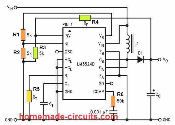
In the above simple SG3524 boost converter design we can see the collectors of the internal driver BJTs CA and CB are joined together for enforcing the ON/OFF switching of the inductor L1 through an appropriately calculated PWM rate.
The PWM rate is set by configuring the SG3524 error amp inputs INV and NI, which is internally set as a comparator, and whose output controls the output PWM.
Setting up the Error Amp for PWM Control
Configuring the error amp is basically implemented by calculating the potential dividers at the INV input through the feedback RF resistor and associated 5 k divider resistor (R3 and R4 shown in green).
This feedback potential at the INV input determines the output pulse cut-off threshold, and the PWM duty cycle.
This threshold limit is fixed with reference to the sample voltage set at the NI input of the error amp through the two 5 k resistors (R1, R2 shown in orange).
Calculating the Feedback Resistor
RF = 5k [(VO / 2.5) -1] = 5000 [(VO / 2.5) -1] this equation sets up the feedback resistor for the PWM control, using the parameters VO = output step-up voltage, and R3 = 5 k.
Calculating Oscillator Frequency
fOSC = 1 / RT * CT this equation sets up the frequency of the converter, which must be anywhere around 30 to 100 kHz. Higher frequencies will mean small L1 inductor.
Calculating the Inductor
L1 = 2.5VIN2 (VO - VIN) / fOSC * IO* VO2 this equation help us to determine the inductance rating for the L1 inductor, using the parameters VIN = input supply voltage, the VO = output voltage, f OSC = frequency, and the IO = output current
Calculating the Output Capacitor
CO = IO(VO - VIN) / fOSC * ΔVO * VO this equation helps us to calculate the output filter capacitor CO, using the parameters IO = output current, VO = output boosted voltage, VIN = input supply voltage, fOSC = frequency, ΔVO = peak-to-peak output ripple.
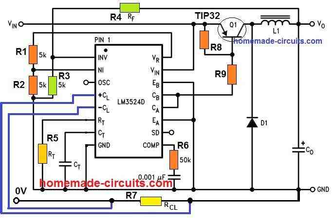
High Current Step Up Converter
In the above DC to DC step-up converter circuit, I have explained how the SG3524 could be configured as a low current step up current without involving external power transistors.
The next diagram below shows how the same concept could be upgraded to a high current DC to DC boost converter circuit using the very same SG3524 circuit, except the output stage where high power transistors are used for facilitating the required current amplification.
This circuit can be used for stepping up or boosting any low voltage (above 5 V) to a desired higher level, without any limitations in the current level.
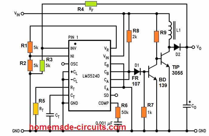
The calculations will be the same as the previous concept.
R9 will depend on the output current spec of the converter, and could be calculated using the formula:
R9 = (VIN - 0.7) * hFE / Max IO
Here, VIN is the input supply voltage, hFE is the current gain of TIP3055, and IO is the maximum output current.
Step-Down Buck Converter using SG3524
The next DC to DC converter circuit using SG3524 discussed below is a step down buck converter which will allow you to convert any higher level DC voltage (below 40 V) into a desired lower DC output voltage, but with an input current not exceeding 80 mA.
Meaning, suppose you are trying to make a 48 V inverter, in which the oscillator circuit can work only with a regulated 15 V DC. In such a situation you can effectively apply this buck converter concept for stepping down 48 V to 15 V DC for powering the oscillator circuit safely and allowing the 48 V to be used by the inverter power devices and the transformer.
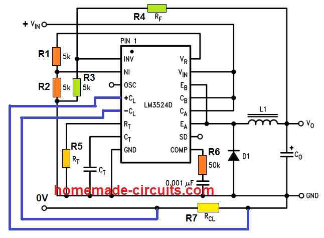
In this configuration we find the IC SG3524 pinout features are configured in the following manner:
The emitters EA and EB of the ICs output transistors are joined together for driving the inductor L1, while the collectors CA and CB are joined together with the input supply Vin for supplying the current to the L1 via the emitters.
The feedback resistor RF (R4) along with the associated 5 k divider resistor R3 is configured as before with the error amplifier, while the reference to the error amp is rigged using R1, R2 via the +5 V supply from the VR (VREF) pin of the IC. This takes care of the PWM control.
High Current Step-Down Converter
In the above example I have explained the low current version of the SG3524 DC step-down converter, without involving external power devices.
For higher current levels, an external power switching transistors could be added, along with other upgraded components such as the L1 inductor and diode.
Meaning, this design can be used for converting any voltage below 40 V to a desired lower level, without any restrictions on the output current level.
An example design for this can be witnessed in the following diagram:
Calculations
The various equations and calculations involved in this SG3524 buck converter circuit can be learned as given below:
Calculating the Feedback Resistor
RF = 5 k [(VO/2.5) - 1] 5000 [(VO/2.5) - 1], this equation is used for fixing the feedback resistor RF(R4) which controls the output PWM
Calculating the Current Sensing Resistor
RCL = Current Limit Voltage / IO(MAX), this equation is used for evaluating the current sensing resistor RCL or the R7, with respect to the maximum desired output current limit IO(MAX) .
The current limit voltage refers to the desired voltage drop that needs to be developed across RCL when IO(MAX) is reached. This current limit voltage could be anywhere between 0.3 V to 1 V, the smaller the better to ensure a smaller RCL
Calculating the Oscillator Frequency
fOSC = 1 / RT*CT this equation allows us to set up the oscillator frequency of the converter, and this can be anywhere between 30 kHz and 100 kHz. Higher frequencies will cause the L1 to be smaller and vice versa.
Calculating the Inductor
L1 = 2.5VO (VIN - VO) / IO*VIN*fOSC this equation can be used for determining the inductor L1 value which becomes the crucial element of the step down converter. In this equation, VO is the desired stepped down output voltage, VIN is the input supply voltage, IO is the maximum output current, fOSC is the oscillator frequency.
The 2.5 value is acquired from the reference voltage formed by the resistive divider using the two 5 k resistors R1, R2 at the NI input of the SG3524 IC error amp.
Calculating the Output Capacitor
CO = (VIN - VO) VO* T2 / 8 *ΔVO *VIN*L1, this equation facilitates determining the output filter capacitor CO, using the available data such as the input supply VIN, output stepped down voltage VO, output peak to peak ripple voltage ΔVO, the inductance of L1, and the period T2 where T = 1 / fOSC
Current Control
In this buck converter we additionally see that current sensing pinouts +CL and -CL of the SG3524 are configured for implementing output current limiting, or for delivering a constant current output for the converter.
The +CL and -CL current limit op amp provides a quick facility to configure the current limiting feature, which overrides all other control feature in the SG3524 IC. Meaning, if the current control feature detects an over current situation, it will override all other features and try to shut down the output of the IC.
Why Over-current shut down is Important in Buck Converter
We already know that the efficiency of this SG3524 buck converter will be very high, may be around 95%. This implies that if the output voltage is stepped down, will result in the output current to rise proportionately.
As an example, suppose we have VIN = 35 V, and we want the output to be VO = 5 V.
If we assume the input current to be 80 mA for the above design, will mean an input wattage = 2.8 watts. This also means that ideally the output current should be then 2.8 / 5 = 560 mA.
Considering the 95 % efficiency, this current still will be in the vicinity of 532 mA, which is a whopping 7 times higher than the input current.
Due to this current boost, a current limiting or current control feature becomes crucial in these step down DC to DC converter designs.
Application
The main application of an SG3524 or LM3524 DC to DC converters can be found in the field of solar controllers.
Solar panels are mostly available with high voltage, low current specs, while batteries are mostly manufactured with lower voltage, higher current (Ah) specifications.
A step-down buck converter becomes highly suitable for integrating a high voltage, low current solar panels with a high Ah, low voltage battery, and ensures a highly efficient and convenient way of implementing solar battery charging.
Courtesy: Texas Instruments


Comments
hi mr swag .. good circuit as usual. i am working on a pulse motor with a power consumption of 63uW maks (4.2Vx15uA), I am using a reed switch after the coil. I tried to use a simple Joule Thief by adding a capacitor paralleled to the reed switch (without transistor) and connect a small fan as a load, power consumption become 50mA. What your opinion which of the circuits in your library is the best for low input power consumption but high output power. thanks mr swag. (Sorry for my english).
-MpiQ-
Hello MpiQ, the output power will be always lower than the input power supply (watts). This cannot be reversed!