The proposed push button timer circuit module can be directly integrated with any existing switch contacts of a lamp and enable the lamp to be converted into a timer controlled lamp.
A common problem arises whenever one wants to replace a mains AC lamp controlled by a switch with a timer or a time switch. Indeed, the wiring that leads to the switch generally does not include the necessary third wire. So instead of tearing the wallpaper in search of junction boxes or even drilling the plate, we offer you a delay OFF timer circuit that can be simply connected in place of the existing lamp ON/OFF switch.
By pressing the push-button, the controlled light turns on. It automatically turns off after an adjustable duration of 1 to 15 minutes. The setup also includes an adjustable circuit breaker that cuts off the device in case of overcurrent or short circuits.
Timer/circuit breaker setup

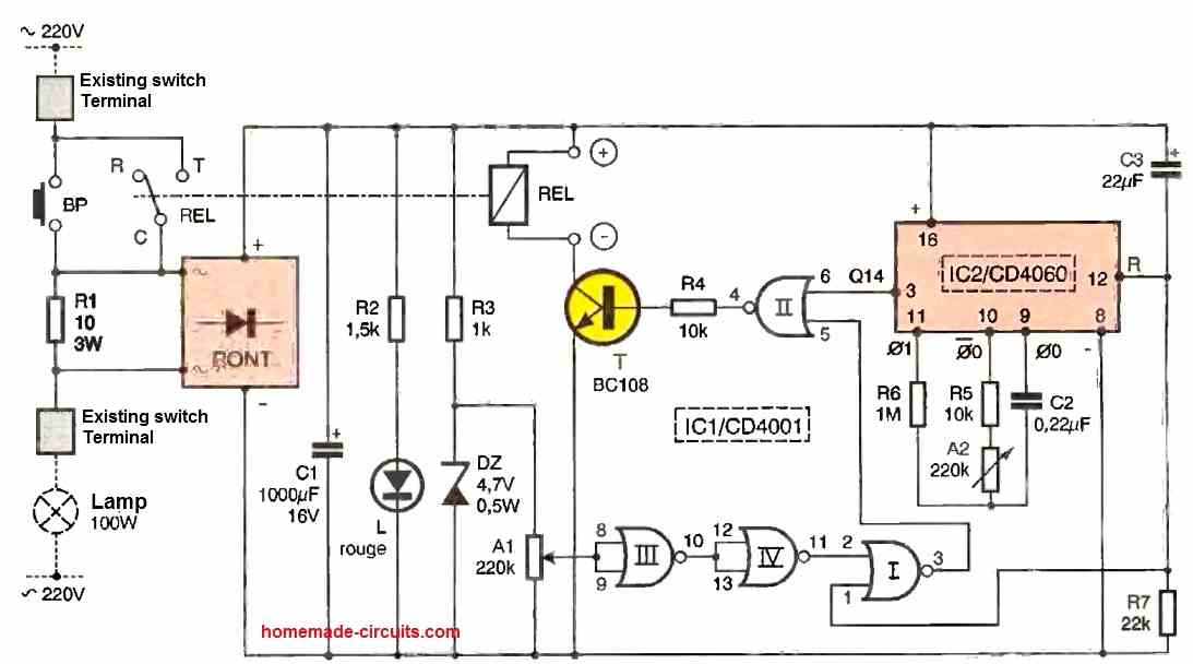
The power supply is derived from the 220 V mains by implementing a 10 W dropper resistor in series with the bulb's power supply. Thus, it is a self-powering arrangement.
For a 100W bulb, the effective current absorbed is calculated as follows: P/U = 100 W / 220 V = 0.454 A.
This current results in a voltage drop across resistor R1 given by: R x I = 10 Ω x 0.454 A = 4.54V.
This is an effective voltage. The peak values of the alternating current are determined by the relationship: Ueff √2 = 4.54 V x √2 = 6.42 V.
The two alternating currents are rectified by the bridge of diodes.
Considering the diode junction potential values in the bridge configuration, a potential of 1.2V (twice the junction potential of a silicon diode, i.e., 2 x 0.6V) should be subtracted from the previously calculated value.
This leaves us with a quasi-continuous potential, primarily determined by C1, of approximately 5.2 V.
LED L1, whose current is limited by R2, indicates the activation of the setup.
The power dissipated by R1 can be determined by the relationship: P = U x I = 4.54V x 0.45A = 2W.
We have chosen a 3W power rating for R1.
It should also be noted that the minimal voltage drop caused by R1 has no effect on the power supply to the bulb.
How the Timer Works
By pressing the push-button connected in parallel with the contacts of the load relay, power is supplied to the circuit.
The integrated circuit IC2, which is a 14-stage binary counter, becomes operational immediately. Upon power supply establishment, capacitor C3 charges through R7, resulting in a brief positive pulse at the RESET input of CD4060, causing a reset initialization.
In particular, the Q14 output is in a low state. Initially, we assume that the output of NOR gate I is low, which is the normal case as we will see later.
Consequently, the output of NOR gate II is high, saturating transistor T. The collector circuit of T includes the coil of a 1RT relay, which immediately closes.
Thus, when the push-button is released, the power supply continues to be self-maintained. It should be noted that the used SIEMENS relay includes an internal diode connected across its coil terminals.
Its purpose is to protect transistor T from the effects of self-induced voltage spikes that primarily occur during power interruptions. As a result, the relay coil is polarized.
The IC2 circuit features an oscillator, and the base period, which characterizes the square wave available at pin 9, is adjustable based on the angular position of adjustable resistor A2.
At the minimum resistance position, this base period is approximately 4.8 ms, while it increases to 56 ms at the maximum resistance position.
The period of the square wave signal at the Q14 output is determined using the equation: T = 214 x T0 (where TO represents the period measured at pin 9).
The duration after which the Q14 output goes high is equal to half of the aforementioned period, i.e., T0 x 213.
Thus, depending on the angular position of the A2 resistor, this duration can be adjusted from 40 seconds to 15 minutes.
After this time interval, the Q14 output of IC2 transitions to a high state. As a result, the NOR gate II output goes low.
Transistor T becomes non-conductive, and the load relay opens. The power supply to the circuit ceases, and the lighting turns off.
Over Current Circuit Breaker
A 4.7V zener diode (DZ) is connected in series with R3 in the circuit's power supply. As a result, a potential of 3.3V is available at its terminals.
Using the adjustable resistor, it is possible to extract a more or less significant fraction of this value.
As an example, let's assume that the angular position of the A1 cursor is such that at the combined inputs of NOR gate III, the measured potential is 2.8V.
With a power supply potential of 5.2V, the value of 2.8V is higher than half of the supply voltage, indicating that the inputs of the NOR gate are considered to be in a high state.
Consequently, the output of NOR gate III is low. The output of gate IV is high, and the output of NOR gate II is low. This represents the normal situation.
Now, let's imagine that an overcurrent occurs in the lighting bulb's power supply or that the power of the bulb is too high (e.g., two 100W bulbs).
In such a situation, the power dissipated in R1 would become excessive, not to mention the fact that the introduced voltage drop would start to affect the brightness of the bulbs.
In this case, the power supply potential of the circuit increases. It might, for example, rise to 8V.
However, thanks to the zener diode, the potential level at the combined inputs of NOR gate III remains locked at the previously mentioned 2.8V, which is now a value lower than half of the power supply voltage.
The output of gate III then goes high. The same happens with the output of gate I.
The output of NOR gate II goes low. Transistor T becomes non-conductive, and the relay turns off. The device reacts as a circuit breaker.
During the power-up of the lighting bulb, when its filament is cold, there is always a brief current surge that could lead to a disruption.
However, this disruption does not occur because the initialization pulse caused by the charging of C3 through R1, mentioned in the previous paragraph, neutralizes the consequences of this overcurrent detection by temporarily forcing the output of NOR gate I to a low state.
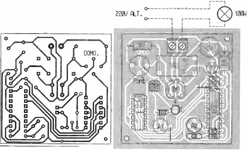
PCB Design


Comments
Great article — your walkthrough of converting a regular AC lamp into a timer controlled fixture is clear and practical. The section covering how pressing the push‑button turns the lamp on and then it automatically turns off after a set time (1 to 15 minutes) is especially useful.
Thanks for your kind feedback, glad you liked the post…