When an inverter with square wave AC output is modified to generate a crude sinewave AC output, it is called a modified sine wave inverter.
The following article presents interesting modified sine wave inverter designs with exhaustive descriptions regarding its construction procedure, circuit diagram, waveform output and detailed parts lists. The designs are intended for learning and building experimental projects by engineers and students.
Here I have explained different varieties of modified designs ranging from a modest 100 watt to a massive 3 Kva power output model.
How Modified Inverters Work
Folks who are new to electronics may get a bit confused regarding the difference between a square wave and a modified square wave inverter. It may be understood through the following brief explanation:
As we all know an inverter will always generate an alternating current (AC) similar to our domestic AC line voltage so that it can replace it during power failures. An AC in simple words is basically a rise and fall of voltage of a particular magnitude.
However, ideally this AC is supposed to as close as possible to a sinewave as shown below:
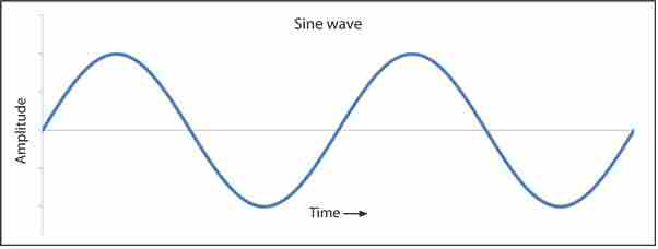
Basic Difference between Sine waveform and Square Waveform
This rise and fall of voltage happens at a particular rate i.e. at a particular number of times per second, known as its frequency. So for example a 50 Hz AC means 50 cycles or 50 ups and downs of a particular voltage in one second.
In a sine wave AC as found in our normal domestic mains outlet the above rise and fall of voltage is in the form of a sinusoidal curve, i.e. its pattern gradually varies with time and thus is not sudden or abrupt. Such smooth transitions in the AC waveform becomes very suitable and a recommended type of supply for the many common electronic gadgets like TVs , music systems , Refrigerators, motors etc.
However, in a square wave pattern the voltage ups and downs are instant and sudden. Such immediate rise and fall of potential creates sharp spikes at the edges of each wave and thus becomes very undesirable and unsuitable for sophisticated electronic equipment. Therefore it is always dangerous to operate them through a Square weave inverter supply.
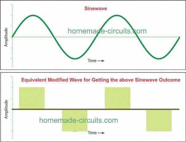
Modified Waveform
In a modified square wave design as shown above, the square waveform shape basically remains the same but the size of each section of the wave-form is appropriately dimensioned so that its average value matches closely to an AC waveform’s average value.
As you can see there's a proportionate amount of gap or null areas between each square blocks, these gaps ultimately help to shape up these square waves into sinewave like output (albeit crudely).
And what is responsible for adjusting these dimensioned square waves into sinewave like features? Well, it is the inherent characteristic of the transformer's magnetic induction which effectively carve the "dead time" transitions between the square wave blocks into a sinewave looking waves, as shown below:
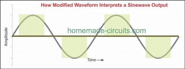
In all the designs I have explained below we try to implement this theory and ensure that the RMS value of the square waves are appropriate controlled by chopping the 330V peaks into 220V modified RMS. The same can be applied for 120V AC by chopping down the 160 peaks.
How to Calculate through Easy Formulas
If you are interested to know how to calculate the above modified waveform so that it results in an almost ideal replication of a sinewave, then please refer to the following post for the complete tutorial:
Calculate Modified Square Wave RMS Sine Equivalent Value
Using IC 4017
Let's investigate the first modified inverter design which is rather simple and uses a single IC 4017 for processing the required modified waveform.
If you are looking for an easy to build modified sine wave power inverter circuit, then perhaps the following concept will interest you. It looks astonishingly simple and low cost with an output that’s to a very extent is comparable with other more sophisticated sine wave counterparts.
We know that when a clock input is applied to its pin #14, the IC produces a shifting cycle logic high pulses through its 10 output pins.
Looking at the circuit diagram we find that the pin outs of the IC are terminated to supply the base of the output transistors such that they conduct after every alternate output pulse from the IC.
This happens simply because the bases of the transistors are connected alternately to the IC pin outs and the intermediate pin-out connections are just eliminated or kept open.
The transformer windings which are connected to the transistor’s collector respond to the alternate transistor switching and produce a stepped up AC at its output having a waveform exactly as shown in the diagram.
The output of this Modified sine wave power inverter is although not quite comparable to the output of a pure sine wave inverter but definitely will be far better than that of an ordinary square wave inverter. Moreover the idea is very easy and cheap to build.
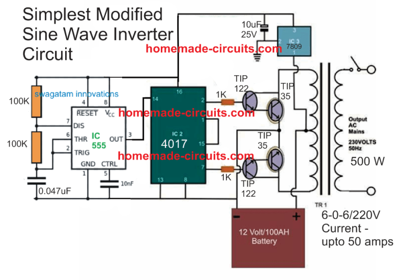
WARNING: PLEASE CONNECT PROTECTION DIODES ACROSS THE COLLECTOR EMITTER OF THE TIP35 TRANSISTOR (CATHODE TO COLLECTOR, ANODE TO EMITTER)
UPDATE: As per the Calculations presented in the this article, the IC 4017 output pins could be ideally configured for achieving an impressive looking modified sinewave inverter.
The modified image can be witnessed below:
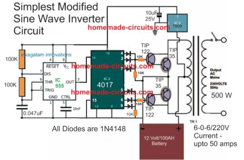
WARNING: PLEASE CONNECT PROTECTION DIODES ACROSS THE COLLECTOR EMITTER OF THE TIP35 TRANSISTOR (CATHODE TO COLLECTOR, ANODE TO EMITTER)
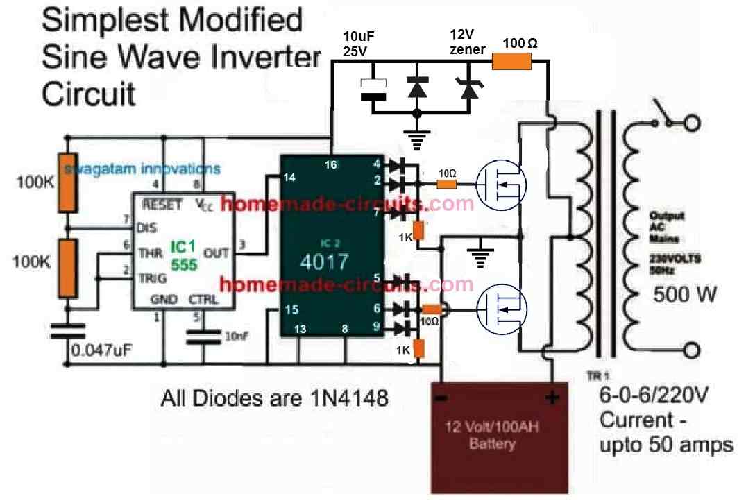
A MOSFET version of the above design can be witnessed in the following diagram. Using MOSFETs IRF3205 can allow the inverter to handle above 400 watts.
Video Demo:
Minimum Specifications
- Input: 12V from Lead Acid Battery, for example 12V 7Ah battery
- Output: 220V or 120V depending on transformer rating
- Waveform : Modified sinewave
Feedback from one of the dedicated viewers of this blog, Ms Sarah
Hello Swagatam,
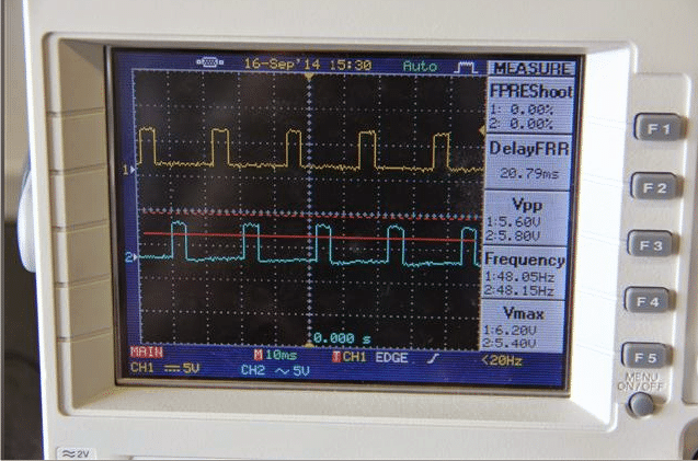
This is what I obtained from the output of IC2 post resistors R4 and R5. As I earlier said I expected to have a bipolar wave. One in positive and the other in negative . to simulate an ac wave cycle. I hope this picture will help. I need a way forward please.
Thanks
My Reply:
Hello Sarah,
The IC outputs will not show bipolar waves since the signals from these outputs are intended for identical N type transistors and from a single supply....it's the transformer which is responsible for creating the bipolar wave at its output since it's configured with a push-pull topology using a center tap ....so what you are seeing across R4 and R5 are correct waveform. Please check the waveform at the output of the transformer for verifying the bipolar nature of the waveform..
Using only 3 IC 555
The following section discusses best modified sine wave inverter circuit with waveform images, confirming the credibility of the design. The concept was designed by me, the waveform being confirmed and submitted by Mr. Robin Peter.
The discussed concept was designed and presented in a few of my previously published posts: 300 watt sine wave inverter circuit, and 556 inverter circuit however since the waveform were not confirmed by me the relevant circuits weren't completely foolproof.Now it's been tested, and waveform verified by Mr. Robin Peter, the procedure revealed one hidden flaw in the design which has been hopefully sorted out here.
Let's go through the following email conversation between me and Mr. Robin Peter.
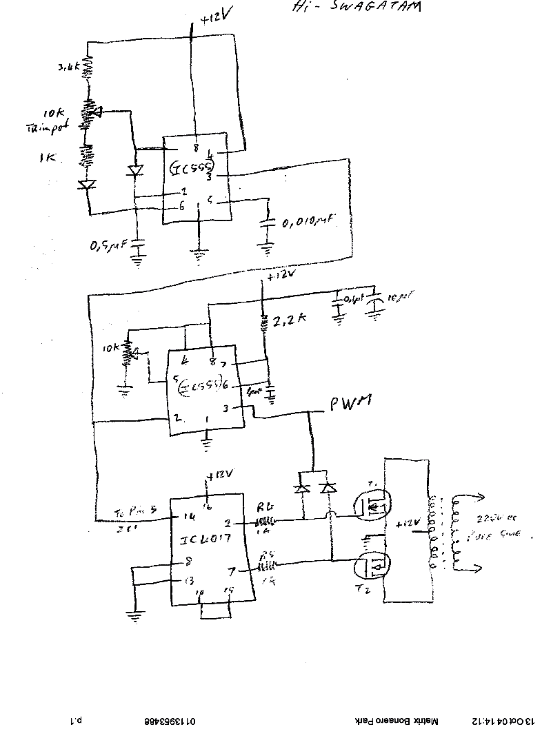
I built the simpler modified sine wave alternative version IC555's,with no transistor. I changed some of the values of the resistors and caps and did not use[D1 2v7,BC557,R3 470ohm]
I joined Pin2&7 of IC 4017 together to get the required waveform. IC1 produces the 200hz 90% duty cycle pulses(1 image), which clock IC2 (2-images) and therefore IC3(2 images, min duty cycle & max D/C)Are these the expected results, My concern is that it is a modified sine where you can vary the
RMS,not a pure sine
Regards
Robin


Hi Robin,
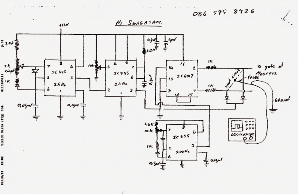
Your modified sine wave circuit diagram looks correct but the waveform isn't, I think we'll need to use a separate oscillator stage for clocking the 4017 with frequency fixed at 200Hz, and increase the frequency of the topmost 555 IC to many kHz, then check the waveform.Regards.
Hi Swagatam
I have attached a new circuit schematic with the changes you suggested along with the resultant wave forms.What do you think of the PWM waveform,the pulses don't seem to go all the way down to ground
level.
Regards


Hi Robin,
That's great, exactly what i was expecting, so it means a separate astable for the middle IC 555 must be employed for the intended results....by the way did you vary the RMS preset and check the waveforms, please do update by doing so.
So now it looks much better and you can go ahead with the inverter design by connecting the mosfets.
....it's not reaching the ground due to the diode 0.6V drop, I assume....Thanks very much
Actually a much easier circuit with similar results as above can be built as discussed in this post:https://www.homemade-circuits.com/2013/04/how-to-modify-square-wave-inverter-into.html
More Updates from Mr. Robin
Hi Swagatam
I varied the RMS preset and here are the attached waveforms.I would like to ask you what amplitude of triangle wave can you apply to pin 5,and how would you synchronise it so that when pin 2 or 7 go + the peak is in the middle
regards Robin


Here's some better modified sine waveform, maybe the guy's will understand them easier. It's up to you whether you publish them.
By the way i took a 10uf cap from pin2 to 10k resistor to .47uf cap to ground.And the triangular wave looked like this(attatched).Not too triangular,7v p-p.
I will investigate the 4047 option
cheers Robin


Output Waveform across Transformer Mains Output (220V)The following images show the various waveform images taken from across the output mains winding of the transformer.
Courtesy - Robin Peter
No PWM, no Load

No PWM, with load

With PWM, without load

With PWM, with load

The above image magnified

The above waveform images looked somewhat distorted and not quite like sinewaves. Adding a 0.45uF/400V capacitor across the output drastically improved the results, as can be witnessed from the following images.
Without load, with PWM ON, capacitor 0.45uF/400v added
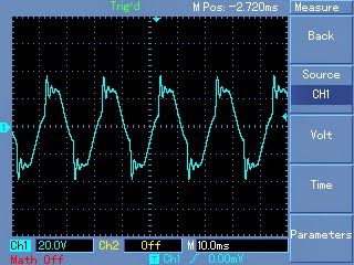
With PWM, with load, and with an output capacitor, this looks very much like an authentic sinewaveform.
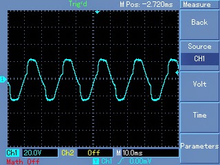
All the above verification and testing were conducted by Mr. Robin Peters.
More Reports from Mr. Robin
Ok,I did some more testing and experimenting last night and found that if I increase the batt voltage to 24v the sinewave did not distort when I increased the duty/cycle.( ok,I've regained my confidence)I added that 2200uf cap between c/tapp and ground but that made no difference to the output waveform.
I noticed a few things that were taking place,as I increased the D/C the trafo makes a noisy humming sound(as if a relay is vibrating back and forth very quickly),The IRFZ44N's get hot very quickly even with no loadWhen I remove the cap there seems to be less stress on the system.The humming noise is not so bad and the Z44n's don't get so hot.[of course no sinewave}
The cap is across the output of the trafo not in series with one leg. I took (3 different windings) round inductors{I think they are toriodal} out of a switch-mode power supply.The result was no improvement in the output wave(no change),
The trafo output voltage also dropped.
Automatic Feedack
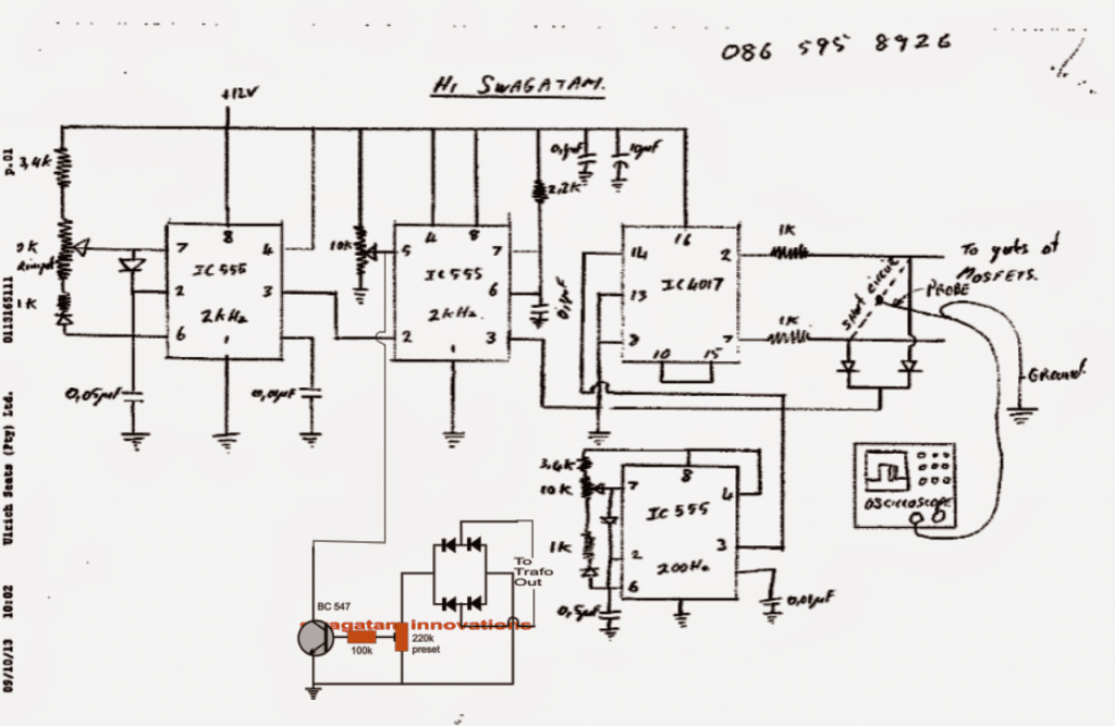
Adding an automatic load correction feature to the above modified sine wave inverter circuit idea:
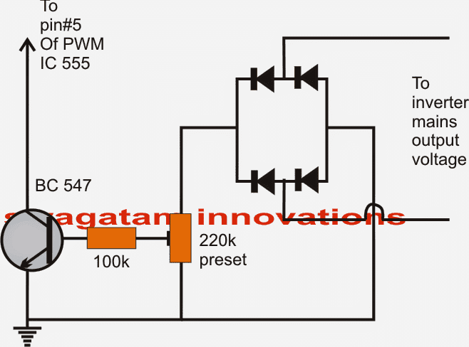
The above shown simple ad-on circuit can be used for enabling automatic voltage correction of the inverter output.
The fed voltage across the bridge is rectified and applied to the base of the NPN transistor. The preset is adjusted such that at no load the output voltage gets settled at the specified normal level.
To be more precise, initially the above preset should be kept at the ground level so that the transistor says switched OFF.
Next, the 10k RMS preset at pin#5 of the PWM 555 IC should be adjusted to generate around 300V at the transformer output.
Finally, the load correction 220K preset should be realigned to bring down the voltage to may be around 230V mark.
Done! Hopefully the above adjustments would be enough for setting up the circuit for the intended automatic load corrections.
The final design might look like this:
Filter Circuit
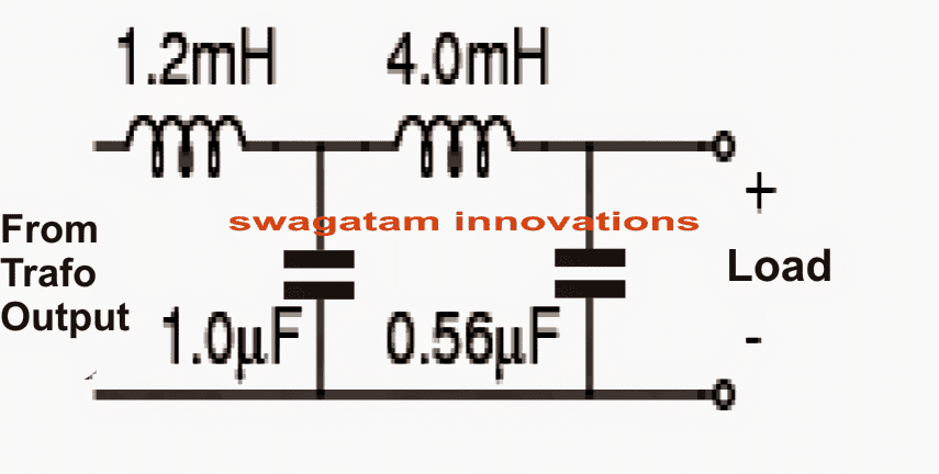
The following filter circuit can be employed at the output of the above inveter for controlling Harmonics and for enhancing a cleaner sinewave output
More Inputs:
The above design was studied and further improved by Mr Theofanakis, who is also an avid reader of this blog.
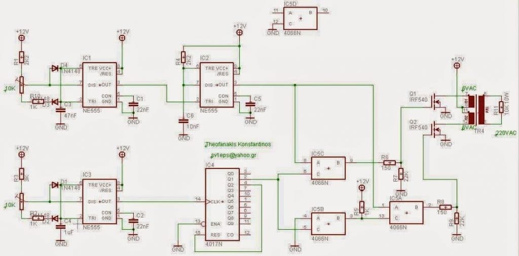
The oscilloscope trace depicts the modified waveform of the inverter across the 10k resistor connected at the mains output of the transformer.
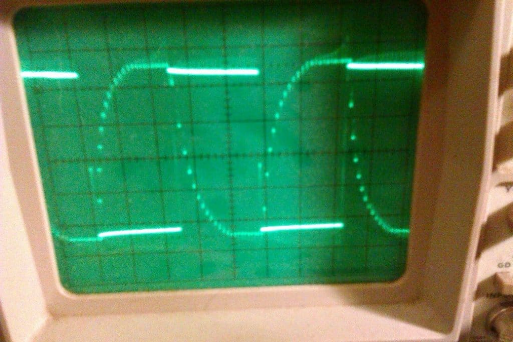
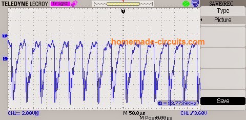
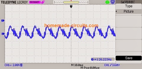
The above modified inverter design by Theofanakis inverter was tested and approved by one of the avid followers of this blog, Mr. Odon. The following test images by Odon confirm the sinewave nature of the above inverter circuit.
Heavy Duty 3Kva Modified Inverter Design
The below explained content investigates a 3kva sine wave inverter circuit prototype made by Mr. Marcelin using only BJTs instead of the conventional mosfets. The PWM control circuit was designed by me.
In one of my previous posts I have explained a 555 pure sine wave equivalent inverter circuit, which was collectively designed by Mr.Marcelin and me.
How the Circuit was Built
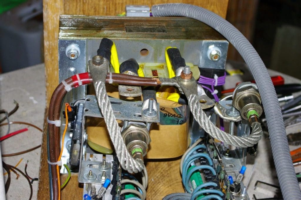
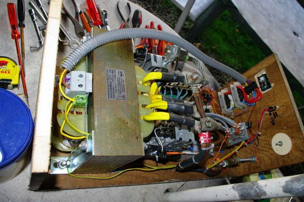
In this design I have used strong cables to sustain the high currents, I used sections of 70 mm2, or more smaller sections in parallel. 3 KVA transformer is actually as solid weighs 35 kg. Dimensions and volume is not a drawback for me. Photos attached to the transformer and installation in progress.
The following assembly nearing completion, based on the 555 (SA 555) and CD 4017
On my first try, with mosfets, earlier this year, I used IRL 1404 which Vdss is 40 volts. In my opinion insufficient voltage. It would be better to use mosfets with a Vdss at least equal to or greater than 250 volts.
In this new installation, I foresee two diodes on the transformer windings.
There will also be a fan for cooling.
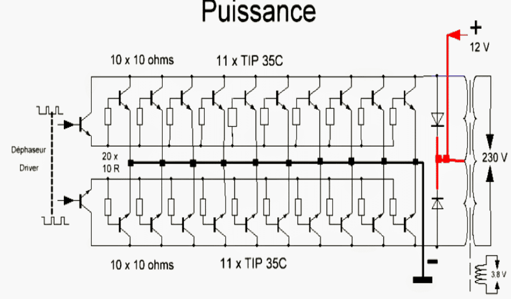
TIP 35 will be mounted by 10 in each branch, like this:
Complete Prototype Images
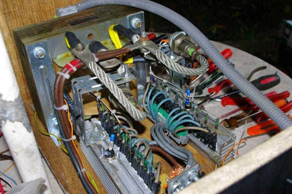
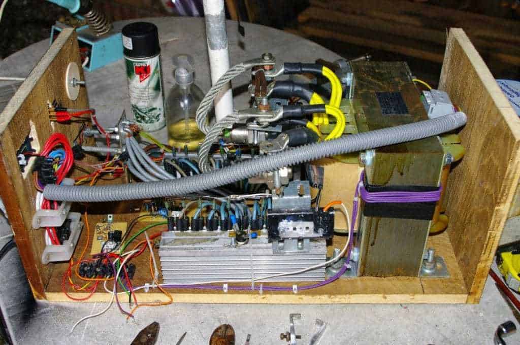
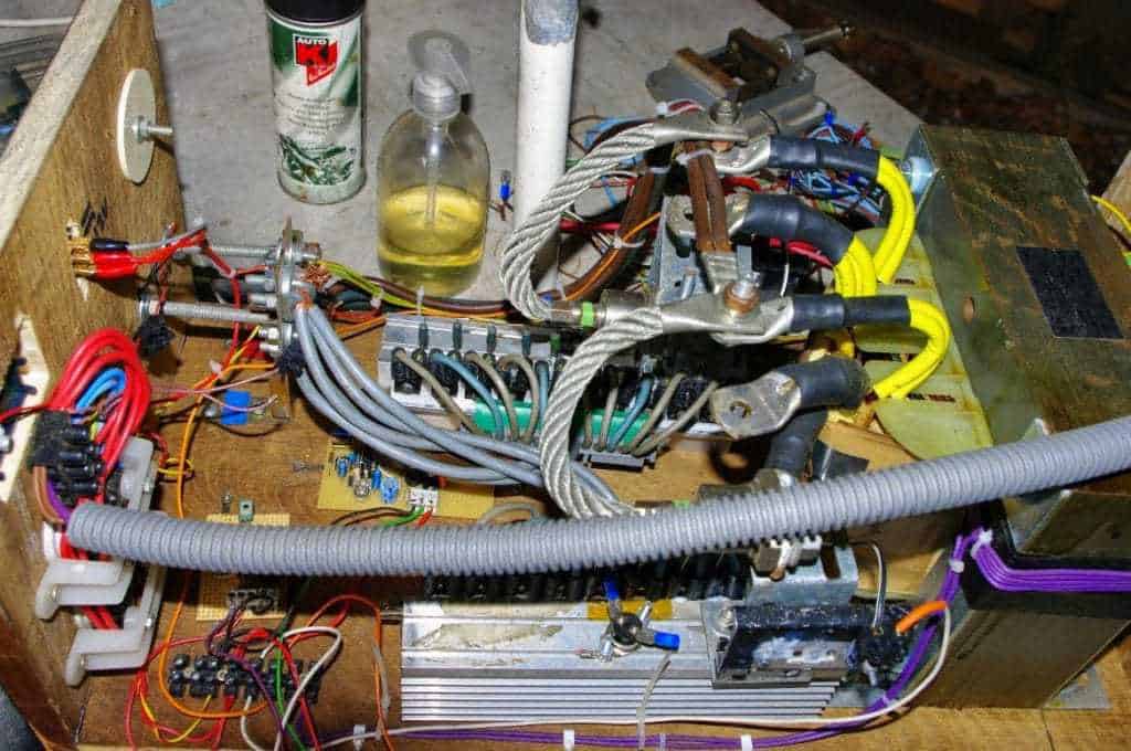
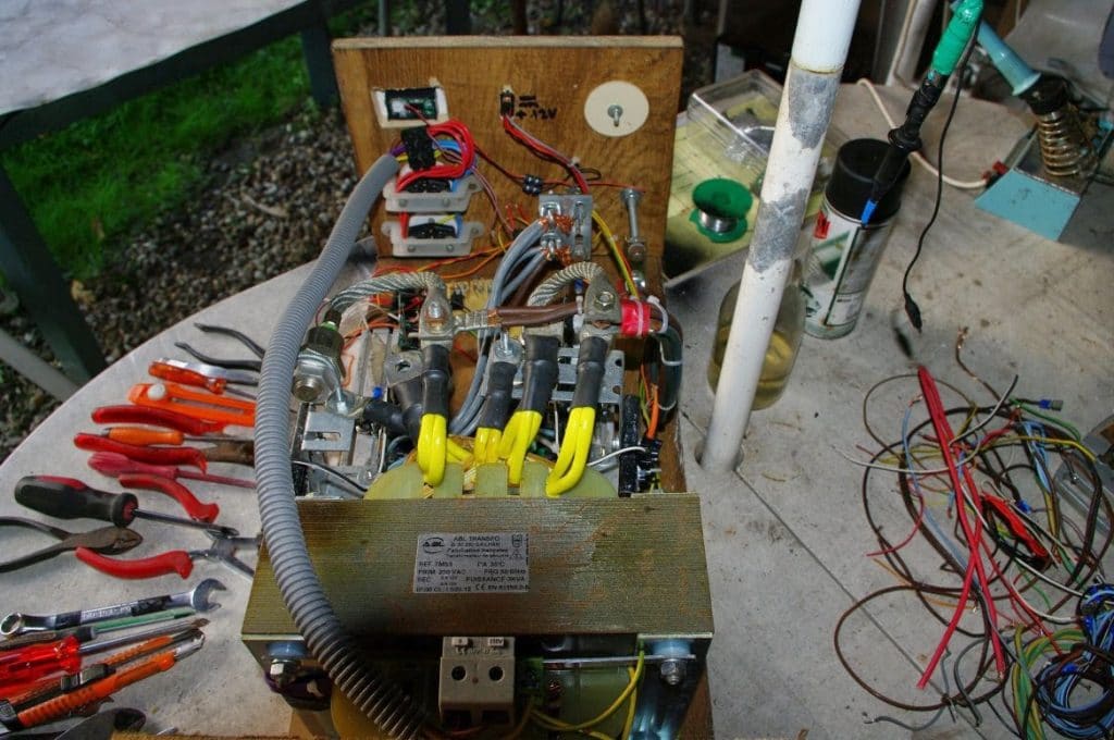
Finalized 3 KVA Inverter Circuit
The final circuit design of the 3 kva modified sine wave inverter should look like this:
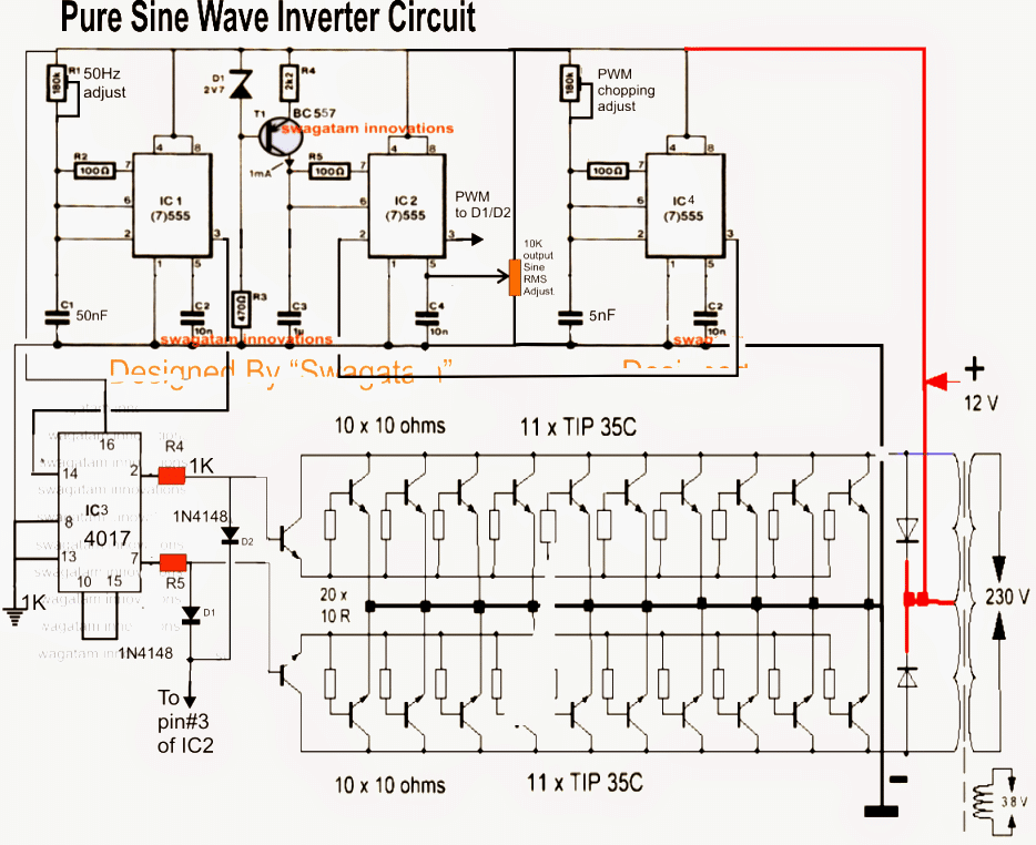
Parts List
All resistors are 1/4 watt 5%, unless specified.
- 100 Ohms - 2nos (value can be between 100 ohm and 1K)
- 1K - 2nos
- 470 ohms - 1no (can be any value upto 1K)
- 2K2 - 1nos (slightly higher value will also work)
- 180K preset - 2nos (any value between 200K and 330K will work)
- 10K preset - 1no (please 1k preset instead for better outcome)
- 10 Ohm 5 watt - 29nos
Capacitors
- 10nF - 2nos
- 5nF - 1no
- 50nF - 1no
- 1uF/25V - 1no
Semiconductors
- 2.7V zener diode - 1no (upto 4.7V can be used)
- 1N4148 - 2nos
- 6A4 diode - 2nos (near transformer)
- IC NE555 - 3 nos
- IC 4017 - 1no
- TIP142 - 2nos
- TIP35C - 20 nos
- Transformer 9-0-9V 350 amps or 48-0-48V / 60 amps
- Battery 12V / 3000 Ah, or 48V 600 Ah
If 48V supply is used then make sure to regulate it to 12V for the IC stages, and supply the 48V only to center tap of the transformer.
How to Safeguard the Transistors
Note: In order to safeguard the transistors from a thermal runaway, mount the individual channels over common heatsinks, meaning use a long single finned heatsink for the upper transistor array, and another similar single common heatsink for the lower transistor array.
Mica isolation would be fortunately not required since the collectors are joined together, and the body being the collector would get effectively connected through the heatsink itself. This would actually save a lot of hard work.
In order to obtain maximum power efficiency, the following output stage is recommended by me, and must be employed with the above explained PWM and 4017 stages.
Circuit Diagram
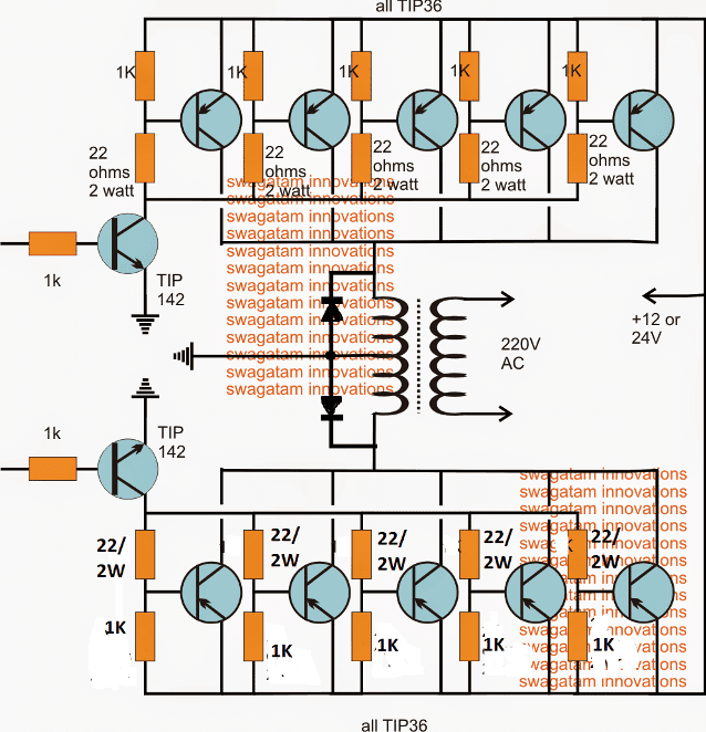
Note: Mount all the upper TIP36 over a larger finned common heatsink, DO NOT use mica isolator while implementing this.
The same must be done with the lower TIP36 arrays.
But make sure these two heatsinks never touch each other.
The TIP142 transistors must be mounted on separate individual large finned hearsinks.




Questions & Answers
gate trigger voltage has no link with drain voltage….5v gate voltage will allow full battery voltage to be pumped into the trafo.
One 50Hz cycle consists of 50 alternate positive and negative peak voltages.
The above pulses are normally in the form of square waves.
The PWMs simply chop the above 50 square waves into thin sections, this results in removing or cutting off some magnitude of the total value of the voltage involved in the original 50 square wave pulses.
We do this to pull down and match the RMS of the pulses with a standard sine pulse.
THe mosfet gate receive the above voltage and switch the battery voltage exactly in the same pattern across the trafo winding through it drain/source leads.
The PWM has no connection with 50Hz switching frequency.
50Hz cycless are created by the alternate switching of the 4017 IC.The PWM are used to break each pulse of the 50Hz cyce into thin calculated sections for setting up the RMS in accordance with a standard sine pulse.
Here the PWM does not depend or need the exact replication of a sine wave, therefore a sine wave input was not felt necessary
My pleasure!
hello Mr Swagatam so this is the wave form u need to feed into the transformer output to produce the desired sine wave output u designed for. Thanks for ur support
hello alex,
yes that's right,
let's thank Mr. Robin for correcting and confirming the facts….
the voltage drop is because of load wattage exceeding the specified normal rating of the inverter (battery power), it's not because of the fets drawing more current, fets only act like switches, they have nothing to do with load current.
No inverter can compensate or increase the output voltage if the load exceeds the maximum allowable capacity, because battery is the ultimate power source beyond which the inverer cannot get anything.
to an extent it may be true, but the above design will also include harmonics(high frequency harmonics) which might cause some noise, although much reduced than an ordinary square wave inverter, it can be removed by additional inductor/capacitor network at the output of the trafo.
pin2 and 7 both will ofcourse produce positive voltages, 50 times each.
the connected mosfets will also conduct accordingly 50 times each but alternately, meaning one after the other and never together, creating 100 alternate positive pulses across the transformer winding.
However the trafo winding polarity being opposite for the two mosfets, the conduction inside the two half winding create positive and negative push pull induction inside the core.
This neg/positive induction gets stepped-up to become positive and negative 50 Hz cycles across the output winding.
so it's the trafo which is responsible for switching the alternate positive pulses from the mosfets into alternate positive and negative AC.
hello Mr Swagatam we all thank mr Robin for his great efforts we anxiously the rest of the project. Would we still use the rest of the circuit that deals with the voltage correction using the bridge rectifier and transistor config. Thank u
Hello Alex,
Voltage correction can be included, depends on the user! However it can be done through an opto coupler stage as discussed in one of my previous posts.
ok mr Swagatam so as soon as he completes his test we would appreciate u to redraw the schematic and give us the final circuit because now we would not know what are the different pot for and how to adjust what u would not know how much of us await ur support keep the good work going sir
surely Mr.Alex…thanks very much, will keep you updated!
thanks! yes you are right, I'll do some research on it and try to put up a related post in this blog soon,
555/4017 = 10mA
4047 = 5mA
it doesn't really matter because mAs won't even scratch the battery anyway.
yes Mr Swagatam I see where uused the optp coupler in the revised version of the inverter but I am not too clear on this because in a post dated August 23 I see where u said this wont help with varing loads please help us here . on this valid point in an inverter. Thank u
I probably said that it won't increase the voltage if load increased above the battery max limits, but otherwise the opto coupler method will certainly do the corrections as per expectation,
anyway i'll try to update the method discussed in the previous comment soon here.
Thank you we await your reply on this because I want to know what gets adjusted when output voltage falls to do the compensating if it is the sine wave pulse width or what. Thank u
I have updated the above article with the required info…pls check it out.
there's a way by using the reset pin#4 of the PWM IC555 as the shut down input.
A sample voltage is derived from the trafo output via a high value preset or voltage divider network and fed to th base of a NPN transistor.
The transistor collector is connected with pin4 of the PWM 555, while the pin4 in turn connected to positive via a 10k resistor.
he preset is adjusted such tat at around 250V, the transistor just begins to conduct. thereby pulling down the reset pin#4 to ground and shutting off the PWMs,
This goes on continuously making sure the output never exceeds the 250V mark.
Hi Marcelin, welcome back.
For making a 3kv system, I am afraid you would have to take care of a few tings, first of all you will have to employ and not transistors, and most importantly a supply voltage more than 50V, actually the higher the better. Also an H-bridge is strictly recommended for such designs, I'll be soon posting a comprehensive design on this soon.
..I meant mosfets and not transistors….
the central 555 which has a 10k preset at its pin5
Go ahead with your feelings and get past your boredom:)… the above design has been proved beyond doubt by Mr. Robin and me, so I think there's hardy any chance that you would fail….moreover we are all eager to see a working prototype of this from somebody.
I'll try to update the required load correction feature here soon.
Actually we could also try connecting the BC547 collector with pin#5 of the PWM IC, as soon as BC547 begins conducting it would tend to bring pin#5 potential towards zero which in turn would result in wide spaces in the output PWMs making the mosfets slower with their conduction.
With mosfets conducting lesser would mean lowering the output voltage and vice versa.
BC547 is NPN, ……….PNP will not work
Hello Mr swagatam have u heard from Mr Robin we need to know how this project work out. I can tell u Hundreds of hobbyist are waiting on ur result because the circuit has been rearranged so many times we really want u to give us a finish circuit with voltage correction circuit included . thank u sir
Hello Alex,
Yes, Mr. Robin has answered positively he would soon build the final design and inform us, let's wait for the results…from my side I can assure you that the above design would definitely work…
Mr Swagatam I see u have updatedthe final drawing and also the voltage correction circuit. we alll appreciate ur support What is the perpose of the 2k pot on the left 555 is it to set the frequency to 2khz. Is the second 555 running at 2khz also. Please tell us the purpose of the 10k pot on the bottom 555 ic. Could u give us a clearer drawing we cannot see the values of some of the components Sir. We are thankful to u sir. I am starting to collect the parts right now sir
Hello Mr Swagatam should we use a small transformer accross the output transformer of say about 12v or so to connect to the bridge rectifiers or connect it straight accross the 220ac volts. Thank u
Hello Mr Alex,
yes the left side 555 control is for adjusting the PWM pulse frequency (thin chopped pillars in the waveform).
The bottom 555 10k control is for adjusting the frequency of the trafo output (50 or 60Hz). The parts are not very critical, slight variation will not matter.
The load correction bridge should be directly connected to the mains output and not thru any additional trafo.
Thank u Mr Swagatam for explaining. So what frequency should we be getting at pin 3 of the left 555 and pin 3 of the middle 555 thank u Sir
2kHz from the left 555, not sure what would be at the output of the middle 555 output because it would be produced after comparing with the triangle waves at the collector of PNP transistor BC557
Hi Marcelin,
With 12V, trying to run a 3KVA inverter would call for hugely thick wires and a massive transformer….everything could get too bulky….and TIP35 is rated at just 25Amps, many of them would be required to cater for the massive 200amps requirement of the design.
Anyway it would be interesting to see how you manage them at your side
You can send me the images to my email ID hitman2008@live.in
thank you Mr Swagatam for ur answer but I am not sure about that transitor u are talking about because i dont see no transistor in the circuit away fro the npn bc457 that is used for the voltage correction only the 4 ic please check I am looking at the circuit above which states ( the final desing might look like this) awaiting ur reply Sir
Hello Alex,
I just missed it, actually Mr.Robin did not use the transistor which existed in the original design at pin6/7 of the middle 555 IC. So as mentioned in the earlier comment here the triangle waves are taken and compared at pin6/7 of the middle 555 IC.
ok Mr Swagatam which circuit should I follow the original design or the last design that Mr Robin has drawn above because I am ready to build the circuit now and tell everyone the results
You can follow the above circuits, designed by Mr. Robin.
The triangle waves are generated by the 555 itself at its pin6/7, so you dont have to feed it externally.
Configure the 555 in a monostable mode….feed a high frequency SQUARE WAVE at its pin2 and sine wave from the bubba at its pin5 ….and now check the result at pin3.
hello mr swagatam could u refer me to any of ur pure sine wave inverter circuits that have been build and tested by any reader because I want to build a working one and try to understand this wave form theory Sir. Thank u and keep up the good work
hello Mr Joel, you can try the above shown design, as you can see the waveforms are verified and they look exactly as assumed by me for the design.
thank u I will try it .so that wave form is the wave form before it drives the fet so how would we get a sine wave at the secondary of the transformer. Thank u
fets will drive the trafo exactly as per the input gate waveform, the waveforms as explained in the above article are optimized sine equivalents which can be verified across the trafo mains output
The calculations are rather simple:
Remember, there's a gap between pin2 and pin7, and also before pin in the 4017 output sequence, which is reducing the duty cycle to 25%.
we can make it to 50% by using pin3, pin2 as the outputs for driving the mosfets, and connect pin4 with pin15 for resetting.
The PWM will obviously reduce the duty cycle by 50%.
That's why I have always recommended using a transformer with input rating 50% less than the batytery voltage, meaning if the battery voltage is 12V, then the trafo must be rated with 6-0-6V input.
The above corrections will solve all the issues suggested by you and present the desired ideal design
According to me the harmonics can be controlled by adding a simple L/C network across the center tap and ground of the transformer…however I am not sure what values would be appropriate, it could be found by a little trial and error.
An example image can be seen here:
Hello Sir,
Question regarding "How to Calculate and Match an Inverter Circuit with Battery and Transformer"
If I use 12v battery,
Max load I need is 25w,
Transformer output = 62.5w,
Transformer current = 62.5/12 = 5.2083A => Used 5A
Battery current = (5.2083/4)+5 = 1.302075+5 = 6.3A => Used 10A,
Now my question is,
What is the maximum backup time in hour(if maximum load connected is 25w)?
Thanks,
Chandrajith
Hello Chandrajith,
I have replied this question in your previous comment.
hello Mr Swagatam with regards to your filter and the link that u refer to on the 3rd Nov 2013 how would this filter be conected from center of transformer to ground because the drawing shows in and out. Dont know if its the right link I saw.. There is a coil in series and a cap accross. Please helpmus here Sir. Thank u
One end of coil to transformer center tap, other to battery positive, capacitor free bottom end to ground.
If you are not comfortable with 6-0-6 tafo then you can increase the battery voltage to 24V and use a 12-0-12 trafo….will give you the same results.
as discussed in the previous comment, use pin3 and pin2 as the outputs from IC4017, and connect only pin4 with pin15 for resetting the IC back to pin3…this will give you 50% duty across cycle at the relevant pinouts.
Hir Sir
I built it with 4017 and I realize that every 1/4 of the 50Hz cycle I have both +,- at this time instead of only + pulses and in the other 1/4 of the 50Hz the – pulses of the modified sine wave. How do you cut the – pulses in the first 25% and the + in the next 25%?
Hi Theofanakis,
The mosfets are responding only for (+) signals from the 4017, and have no connection with (-) signals.
It's the transformer that is responsible for inverting the mosfet signals into (+)/(-), alternately.