These ICs LF155 LF156 LF256 LF257 LF355 LF356 LF357 all belong to one big family of JFET input operational amplifiers. These are special op amps that give very high input impedance, very low input bias current and good DC accuracy. You may think why they made so many numbers, but the reason is that each number has some variation in offset, bandwidth, or noise. So if you are making a circuit that needs low noise then you can pick one type, but if you need higher speed then you can pick another type.
LF3XX IC Family background
This whole LF3XX IC family started as precision JFET input op amps that Texas Instruments and National Semiconductor promoted long back.
That time people needed op amps with very low input currents because bipolar input ones like LM741 were giving trouble for measurement circuits.
So they designed LF155 and LF156 as first generation. Later they came with LF256 and LF257 as improved second generation with better offset and speed.
And after that came LF355 LF356 LF357 that were upgraded for even better performance in noise, offset and slew rate.
Pinout explanation of LF155 LF156 LF256 LF257 LF355 LF356 LF357

So we see in the picture that these ICs can come in two different physical packages. One is the 8-pin TO-99 round metal can package which is written as LMC package, and another one is the common 8-pin DIP or SOIC plastic package which is written as D or P package.
The internal connections are same, only the outer pin numbers are arranged differently because of the package style.
TO-99 8-pin LMC package
Pin 1 is Balance. This is one terminal of offset balance adjustment. You can connect a potentiometer between pin 1 and pin 5 and wiper to negative supply to adjust the output offset voltage.
Pin 2 is Inverting Input. If you connect signal here then it gets inverted at the output.
Pin 3 is Non-Inverting Input. If you connect signal here then it comes at the output in same phase.
Pin 4 is V– which is negative supply. Normally you connect –15 V here.
Pin 5 is Balance. This is second terminal of offset balance pin. Works together with pin 1.
Pin 6 is Output. This is where you get the amplified output of op amp.
Pin 7 is V+ which is positive supply. Normally you connect +15 V here.
Pin 8 is NC which means No Connection. It is not internally connected, you can leave it open.
8-pin DIP or SOIC package
Pin 1 is Balance. Same function as TO-99, one side of offset adjust.
Pin 2 is Inverting Input. Works same as described above.
Pin 3 is Non-Inverting Input. Works same as above.
Pin 4 is V– which is negative supply.
Pin 5 is Balance, the second side of offset null.
Pin 6 is Output.
Pin 7 is V+ which is positive supply.
Pin 8 is NC, no internal connection.
How to use balance pins
Now we can see that there are two pins called Balance, pin 1 and pin 5. These are provided so that you can adjust the input offset voltage.
If you connect a 10 k potentiometer between them with the wiper to V– then you can trim the output offset close to zero. If you do not need offset trimming then you can leave them open.
Important notes about pin usage
You must always connect pin 4 and pin 7 to the proper supply rails. If you leave them floating then the IC will not work.
You must also connect bypass capacitors near the supply pins for stability, like 0.1 µF ceramic to ground.
The input pins 2 and 3 should not be driven beyond the supply rails, otherwise the input JFETs can get damaged. Pin 6 output cannot swing fully to rails, so you should keep some headroom.
Internal IC Structure
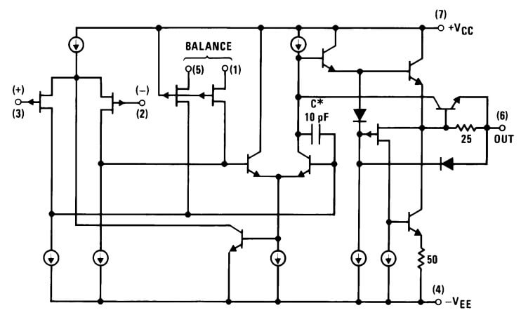
Important features
You will see that these ICs share some common things. They all have JFET input stage so the input bias current is in picoampere range.
That means if you connect them in high resistance sensor circuit then they will not load the signal. The input impedance is very very high, around 10^12 ohm.
The offset voltage is also low depending on grade. The slew rate and gain bandwidth varies between different numbers.
Different IC numbers
Now let us see each one. LF155 is the basic one, it gives good input characteristics but offset is moderate.
LF156 is similar but with tighter specs for offset and bias. LF256 and LF257 are advanced grade versions, LF256 is like LF156 but improved in some parameters, LF257 is like LF155 improved.
Then you have LF355 LF356 LF357, these are newer ones, the LF355 is like LF155 but better noise and offset, LF356 is like LF156 but improved, LF357 is high speed one with higher slew rate.
So basically they are same family but made in different bins so that you can choose according to budget and requirement.
Electrical characteristics table
| Parameter | LF155 | LF156 | LF256 | LF257 | LF355 | LF356 | LF357 |
|---|---|---|---|---|---|---|---|
| Input Bias Current (typ) | 30 pA | 30 pA | 30 pA | 30 pA | 30 pA | 30 pA | 30 pA |
| Input Offset Voltage (max) | 10 mV | 5 mV | 5 mV | 10 mV | 10 mV | 5 mV | 10 mV |
| Input Resistance | 10^12 Ω | 10^12 Ω | 10^12 Ω | 10^12 Ω | 10^12 Ω | 10^12 Ω | 10^12 Ω |
| Gain Bandwidth Product | 2.5 MHz | 2.5 MHz | 5 MHz | 5 MHz | 2.5 MHz | 2.5 MHz | 5 MHz |
| Slew Rate | 13 V/µs | 13 V/µs | 13 V/µs | 13 V/µs | 13 V/µs | 13 V/µs | 50 V/µs |
| Noise (typ) | 25 nV/√Hz | 25 nV/√Hz | 20 nV/√Hz | 20 nV/√Hz | 15 nV/√Hz | 15 nV/√Hz | 15 nV/√Hz |
| Package | DIP, TO-99 | DIP, TO-99 | DIP, TO-99 | DIP, TO-99 | DIP, TO-99 | DIP, TO-99 | DIP, TO-99 |
Absolute maximum ratings of LF155 LF156 LF256 LF257 LF355 LF356 LF357
The following are the absolute maximum ratings of these LF3XX ICs. You must always design the circuit so that the IC works well within these limits. If you cross these limits even once then the IC may get permanently damaged.
Supply voltage V+ to V– : ±22 V maximum. That means the total difference between positive supply and negative supply must not be more than 44 V. Normally you use ±15 V but you should never go beyond ±22 V.
Differential input voltage : ±30 V maximum. This is the maximum voltage that you can put between the two input pins (inverting and non inverting). If you apply more than this then the input transistors may get destroyed.
Input voltage range : V– –0.5 V to V+ +0.5 V. That means the input pins should never be taken beyond 0.5 V outside the supply rails.
Output short circuit duration : Continuous. This op amp can survive shorting the output to ground for continuous time without burning. But still it is not a good practice to do intentionally.
Power dissipation : Depends on package, but typically 500 mW for DIP package at 25°C. The dissipation decreases if temperature rises.
Operating temperature range : 0°C to +70°C for commercial version, –55°C to +125°C for military version.
Storage temperature range : –65°C to +150°C. That means if you store the IC it can tolerate these extreme temperatures.
Lead temperature (soldering, 10 sec) : +300°C. That means if you are soldering the IC leads then the temperature should not exceed this limit for more than 10 seconds.
| Parameter | Maximum Rating |
|---|---|
| Supply Voltage (V+ to V–) | ±22 V |
| Differential Input Voltage | ±30 V |
| Input Voltage Range | V– –0.5 V to V+ +0.5 V |
| Output Short Circuit Duration | Continuous |
| Power Dissipation (at 25°C, DIP) | 500 mW |
| Operating Temperature Range (Commercial) | 0°C to +70°C |
| Operating Temperature Range (Military) | –55°C to +125°C |
| Storage Temperature Range | –65°C to +150°C |
| Lead Temperature (Soldering, 10 sec) | +300°C |
Package details
These op amps normally come in 8 pin DIP or metal can TO-99 package. Pinout is same as standard op amp, pin 2 inverting input, pin 3 non inverting input, pin 4 negative supply, pin 6 output, pin 7 positive supply, other pins offset null.
Important notes
You must remember that these op amps need dual supply like ±15 V for proper operation, though they can run on ±5 V also.
If you operate them with single supply then you have to bias the input properly. Also you must not overdrive the input beyond the supply rails.
They are not rail to rail devices, so you have to keep input and output in safe region.
Applications Circuits
You can use these op amps in circuits where you need low input current, like pH meter, electrometer, photodiode amplifier, medical sensor, instrumentation amplifier, sample and hold, integrator, precision filters.
If you use normal op amp like LM741 in these circuits then it will ruin the accuracy but if you use LF155 family then the results will be very good.
Settling Time Circuit
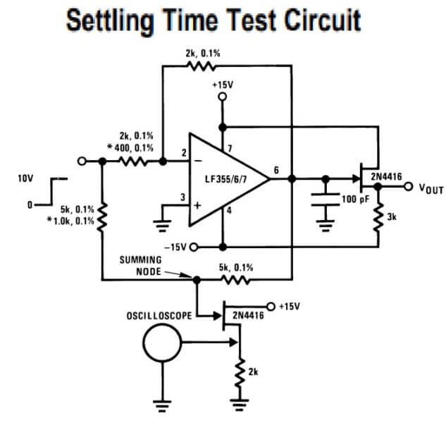
Circuit Description
We see here the op amp LF355 LF356 or LF357 is wired in an inverting amplifier configuration. The non inverting input pin 3 is grounded.
The inverting input pin 2 is connected to the input through a resistor network. You see 10 V step signal is applied through a series resistor, that is 5 k and a switch.
Then there is a 2 k feedback resistor from output back to pin 2. This makes the op amp act like inverter with gain of –5 depending on resistor values. For LF357 they used this –5 gain, for LF355 or LF356 they can use unity gain inverter.
You can also see a 100 pF capacitor from output pin 6 back to the inverting input, in parallel with the 2 k resistor. This small capacitor improves stability and simulates load capacitance. At the output, they added a 3 k resistor to ground which makes proper loading.
Now the output of op amp is connected to a transistor 2N4416 which is a JFET. This JFET is used like a source follower buffer stage.
The reason for this is that the oscilloscope probe itself has capacitance. If you connect the scope probe directly to op amp output then that capacitance will disturb the settling behavior. So they isolate the scope using this JFET buffer.
The oscilloscope input is connected at the source of the JFET with a 5 k resistor from source to the summing node. This way the oscilloscope sees the signal without adding extra loading to op amp output.
The supply connections are standard ±15 V, you can see positive supply to pin 7 and negative supply to pin 4.
How the test works
Here the idea is simple. You apply a sudden 10 V step signal at the input and then the op amp output must jump to the new value according to the gain. For example if gain is –5 then 10 V step in will cause –50 V step out, but since supply is ±15 V, practically it will clip at maximum allowed swing. So usually they keep input step smaller to keep within supply rails.
The oscilloscope is placed at the summing node through the FET isolation, so you can monitor how fast the op amp output settles to final value after the step. This is how they measure settling time specification.
Why so many resistors are precision
We also notice that the resistors are written with 0.1% tolerance. That is because in measurement of settling time, even small error in resistor values can make wrong gain or wrong test condition. So they use precision resistors.
Low Drift Adjustable Voltage Reference

Circuit Description
In the above diagram we see here the op amp LF355 is wired in a feedback arrangement to generate a precise fixed output voltage, around 10 V.
The reason they call it low drift is because the output voltage does not change much when temperature changes. The circuit is made in such a way that ΔVout / ΔT is about ±0.002% per degree Celsius which is very small.
Now let us see the components. The op amp LF355 has its non-inverting input pin 3 connected to a divider made of resistor R1 (180 k) going to ground and potentiometer P1 (250 k) connected up to the JFET 2N4118.
This P1 is called drift adjust. It allows you to tune and cancel out the small offset drift of the op amp with temperature.
The inverting input pin 2 is connected to ground through resistor R1, so the circuit balances itself with help of feedback from output pin 6.
The output pin 6 is connected to a resistor chain R2 (300 k), R3 (180 k) and potentiometer P2 (100 k). This network sets the feedback ratio and hence sets the output voltage.
By adjusting P2 you can precisely set Vout to 10 V or other value you want. That is why they wrote P2 is Vout adjust.
The JFET transistor 2N4118 is used as a constant current element and for temperature compensation. It helps to stabilize the drift of the op amp input.
Because JFET has some temperature behavior that cancels the drift of op amp input bias. So by tuning P1 and using the JFET in feedback, you can make the reference voltage almost immune to temperature.
The supply is simple, you just give +15 V at pin 7 of op amp and ground at pin 4. The output Vout comes at pin 6.
Why all resistors should be wire wound
In the note it is written that all resistors and potentiometers should be wire wound. That is because wire wound resistors have very low temperature coefficient and they do not change value with heat as much as carbon or metal film. If you use normal resistors then the drift will increase. So if you want true low drift performance then you must use wire wound precision resistors.
Why they suggest LF155 also
In the note it is said you can also use LF155. That is because LF155 has even lower input bias current and lower supply current. That makes the drift still lower, so output becomes more accurate and stable.
Fast Logarithmic Converter
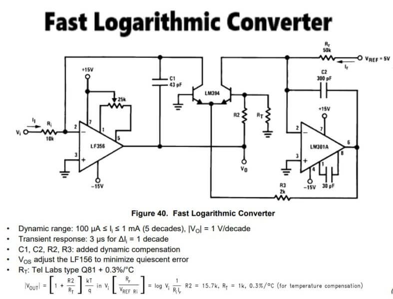
Circuit Description
In the next application circuit above we see this circuit is basically converting an input current into a logarithmic output voltage. It is made to work very fast and to cover many decades of input current. The output gives 1 V per decade of current change.
First stage is the LF356 op amp. Input signal current Ii is generated by feeding input voltage Vi through resistor Ri. The LF356 op amp forces this current into the matched transistor pair inside LM394.
The LM394 is a precision transistor pair, and it converts the input current into a logarithmic voltage because of the transistor exponential I-V law. That log voltage is called Vo.
But only this would not be enough because transistor base-emitter voltage is temperature dependent.
That is why a resistor RT is used for temperature compensation and it is selected as a special thermistor type (Q81, +0.3 %/°C). So Vo becomes temperature stable.
The capacitor C1 (43 pF) around LF356 and the capacitor C2 (300 pF) around LM301A op amp are for dynamic compensation. They make the converter fast and stable so that response time can reach 3 µs for a decade change.
The second op amp LM301A is used as a scaling amplifier. It takes Vo, applies gain adjustment through R2, R3, RT, and then scales the output in such a way that final output is exactly 1 V per decade of input current. The output current through Rf is compared against VREF = 5 V to maintain correct scaling.
The given equation at the bottom shows the output relation.
|Vo| = (1 + R2/RT) × (kT/q) × ln(Vi / (Ri × Ir))
Here Ir is the reference current fixed by VREF / Rf. So basically the circuit is comparing input current to a reference current and taking the log ratio, scaled by kT/q (thermal voltage).
The resistor ratio R2/RT modifies this term to correct for temperature drift.
So in simple words, input Vi is converted into current Ii. That current is processed through matched transistors LM394 to generate a log signal.
Temperature compensation and scaling is applied by RT and R2. LM301A amplifies and scales the result. Final output is a fast logarithmic voltage, 1 V per decade, stable across 100 µA to 1 mA range.
Precision Current Monitor

Now you see in this application we are using the IC like LF155 or LF156 or LF356 family for making a circuit which can sense and monitor the current in a very precise way.
We put a low value resistance called Rs in the path of the load current and then the op amp is configured in such a manner that the voltage drop across this small resistor gets amplified and converted into a useful monitoring signal.
So what we are doing is we let the op amp detect even the tiny voltage difference across Rs and then it will boost it so that you can measure it easily with a voltmeter or feed it to another stage.
We can see that the load is placed in series with the sense resistor Rs. The voltage appearing across Rs is very small because Rs is very low otherwise the load will lose power. But this tiny voltage drop is enough for the op amp to pick.
The op amp here is wired like a differential amplifier so that it can sense the potential difference across the resistor and ignore the common mode part. This is very important because if the circuit did not reject common mode part then the measurement would become useless.
So the current through the load flows also through Rs. When the current is more then the voltage drop across Rs is also more and when the current is less then the drop is also less.
The op amp reads this relation and gives an output voltage that is directly proportional to the current flowing.
So now you can calibrate the system such that the output voltage is equal to some scale of the current, for example you can adjust it so that 1 volt equals 1 ampere, or any ratio you want.
We also note that we can choose Rs according to the maximum load current and the sensitivity we want. If Rs is too high then the load will lose power and if Rs is too low then the op amp will not sense properly. So you must select Rs in between the correct balance.
We also select the op amp feedback resistor values accordingly so that we can get the right gain from the amplifier.
In real life use we can connect the output of this precision current monitor to a measuring instrument, or to a data logger, or to another protection system which will act when the current goes above a certain limit.
For example if the current is too high then you can feed the output to a comparator and then shut down the power supply.
So this circuit is very useful because it gives us accurate current measurement without disturbing the actual load operation and also it allows us to scale the measurement to a safe range.
That is why LF155 and LF356 family op amps are very suitable here because they have low input bias current and very high input impedance which means they do not load the sense resistor.
8-Bit D/A Converter With Symmetrical Offset Binary Circuit

Circuit Description
Now, in this next application circuit here we are having a DAC08 which is basically an 8 bit multiplying digital to analog converter and this one can take in a binary input and then give us a proportional analog output current.
The LF356 op amp is used along with it so that the output current of DAC08 can be converted into a voltage form which is easier for us to use.
The connection is normally done in such a way that the digital input is fed as a parallel binary word into the DAC08 pins. Then the DAC08 generates a corresponding output current which depends on the binary value that we feed.
Now in symmetrical offset binary scheme the input coding is different from the normal straight binary. In straight binary the digital zero corresponds to minimum output and all ones correspond to maximum output.
But in symmetrical offset binary the midpoint of the digital code range corresponds to zero analog output.
So the negative codes give negative analog voltage and the positive codes give positive analog voltage. This is why we call it symmetrical because the zero point is in the center.
The DAC08 produces an output current which is a function of the input binary word and the reference current applied.
So the output current Iout is equal to (Digital Input Value divided by 256) multiplied by Iref. Now since we want voltage, we cannot directly use this current, so we use LF356 op amp which is connected as a current to voltage converter.
The DAC08 current output goes into the summing node of LF356 through feedback resistor and then we get a voltage at the output of LF356. This output voltage is then equal to minus Iout times Rf.
So for symmetrical offset binary coding we arrange the input logic such that the mid code 10000000 represents zero volts output.
Then the code 11111111 gives maximum positive voltage and the code 00000000 gives maximum negative voltage.
Because the op amp has both sourcing and sinking ability through the reference connection, the full swing can be realized. The LF356 is chosen here because it has low input bias current, high slew rate, and can handle high speed DAC operation.
Let us also consider how the symmetry works. When you apply digital code less than mid scale then the DAC output current becomes negative relative to the reference and the LF356 converts that into a negative output voltage.
When we apply digital code higher than mid scale then the DAC output current goes positive relative to reference and LF356 gives you positive output voltage.
This way the transfer function becomes symmetrical around zero point.
So the overall operation is that you feed an 8 bit digital word into DAC08, you apply a proper reference current to DAC08, then the chip produces a proportional output current.
This current is passed into LF356 op amp configured as current to voltage converter, then you get a proportional output voltage.
Because we are using symmetrical offset binary coding the output voltage range is centered around zero so that we can get both positive and negative voltages depending on digital code.
This is how the 8 Bit D A Converter with Symmetrical Offset Binary circuit using DAC08 and LF356 works in practical form.
Wide BW Low Noise, Low Drift Amplifier

In the next diagram above we are seeing an op amp circuit built using LF356. This op amp is chosen because it has low noise, wide bandwidth and also very low drift, so that makes it suitable for precision type of applications.
Now if we look at the connections, the input signal Vin is given through resistor R1 into the inverting pin number 2 of the op amp. The non inverting pin 3 is grounded. That means this configuration is an inverting amplifier type.
We can also see a capacitor C1 connected from pin 2 to ground. This capacitor basically filters out any high frequency noise from the input and stabilizes the input node.
Then in the feedback path from output pin 6 to input pin 2 we can see a resistor R2 and capacitor C2 connected in parallel.
That parallel RC network decides the closed loop gain and also shapes the bandwidth of the amplifier. Resistor R2 sets the main gain, while capacitor C2 bypasses high frequency components so that the amplifier can handle wider bandwidth with stability.
Now the op amp gets its supply from pin 7 (positive V+) and pin 4 (negative V−). The output is taken from pin 6.
According to the note below, the output swing shown is about ±10V sine wave. The maximum frequency up to which this amplifier can handle this swing without distortion is decided by the slew rate of the op amp.
The relation is:
fmax = Sr / (2πVp). For LF356 the slew rate is around 13 V/µs and with a 10 V peak output the calculation gives about 191 kHz maximum frequency. That is why the diagram shows fMAX ≈ 191 kHz.
So overall this circuit is a low noise, low drift, wide bandwidth inverting amplifier using LF356. It is designed for situations where we need clean high frequency amplification up to nearly 200 kHz with stable ±10 V output swing.
C1 and C2 Values
C1 makes problem because it mixes with the feedback resistance R2 and input resistance R1 and that creates a pole in high frequency region. When such high frequency pole comes then the gain falls and amplifier becomes unstable or noisy.
So the solution is to put one small capacitor C2 in the feedback path in parallel with R2. The value of C2 is not random but it must balance the effect of C1. The simple relation is that R2 multiplied by C2 must be equal to R1 multiplied by C1. So the formula is
R2 C2 ≃ R1 C1
That means if input resistor R1 is large and parasitic capacitance C1 is 3 pF then we can calculate the required C2 for feedback. This compensation removes the extra pole and makes the frequency response flat and wide.
So we can say this inverting amplifier using LF356 becomes low noise because of op amp internal design, low drift because offset is small, and wide bandwidth because of this external compensation using C2.
Without C2 the circuit will have peaking and ringing at high frequency but with C2 the amplifier will work smooth even for fast signals.
Boosting the LF156 With a Current Amplifier

Circuit Description
In the figure above we see they are using one LF355 or LF356 op amp and then they are adding one LH0002 current amplifier stage after it.
Now LF356 itself is a JFET input op amp, it is high gain and high input impedance but its output drive capability is not big. It cannot source or sink much current, maybe just a few mA. So if we want to drive a low resistance load, or if we want more current output then it will fail.
That is why they added the LH0002 which is basically a power buffer or current booster IC. This LH0002 can source and sink much higher current, around 150 mA. So it can drive loads like 100 ohm or even less.
Now see the circuit, R1 and R2 form the normal feedback for the op amp stage, so LF356 is just working like a normal amplifier with gain set by R1, R2. Its output is fed into the LH0002 input pin 3. Then LH0002 directly drives the load.
Notice one thing, the feedback R2 is not taken from the op amp pin 6 output but from the final output of LH0002. That means the op amp is forced to correct itself not just for its own output but for the boosted output. This way accuracy and gain are maintained, and distortion is low.
Also you see the supply rails have 0.1 uF capacitors for bypassing, and at the LH0002 output they connected 0.01 uF capacitor in parallel with the load for stability.
So what happens is, the LF356 still controls the voltage gain and linearity, but the heavy current is actually delivered by LH0002, like a muscle amplifier. It can swing the same voltage but with much more current drive.
As per note, the maximum Iout is around 150 mA and the slew rate is around 0.15 / 0.01 = 15 V/µs with the capacitor CL. They also mention no extra phase shift is added because this buffer is unity gain stable.
So in short this circuit is like: LF356 gives the brains, LH0002 gives the muscles. Together they can amplify a small signal into a strong one with good accuracy and enough current to drive low impedance loads.
Decades VCO

Circuit Description
So first we see that the design is using an LF356 op amp, an LM319 comparator and two transistors 2N4092 and 2N4220. This whole thing is working like a voltage controlled oscillator where the control voltage VC decides the output frequency f.
Now let us break it down.
At the left side we see the VC input. This voltage is fed through resistors R1 and R2 into the inverting pin of the LF356 op amp. The non-inverting pin of this op amp is biased with divider R3 and R4 to get a fixed reference point. So the op amp output will basically drive a ramp or integrator action depending on VC input.
Then we see a capacitor C of 0.01uF connected from op amp output back to the input, and also through a 25k resistor feedback network.
This makes the op amp work like an integrator so the capacitor is charged and discharged linearly based on the current controlled by VC. That means the slope of the capacitor voltage depends on VC and that slope will later define the frequency.
Now to create oscillation we need a reset mechanism. That is where the LM319 comparator and the transistors come in.
The LM319 compares the capacitor voltage with fixed thresholds made by R7 and R8 network from ±5V supplies. So as soon as the capacitor ramp reaches one limit, the comparator output toggles.
The comparator output is then fed to the transistor pair Q1 and Q2. Q1 is a 2N4092 (JFET) which acts like a discharge switch and Q2 is 2N4220 which provides current switching.
Together they reset or reverse the charging direction of the capacitor when the comparator changes state. This keeps the ramp going up and down in a repetitive triangular fashion.
So in simple words the capacitor voltage becomes a triangular waveform whose slope depends on the VC input.
The LM319 comparator also produces a clean digital square wave output corresponding to that triangular ramp. This output is pulled up by R5 to +5V so that we get a TTL compatible square wave at f output.
Now looking at the passive parts: R6 and R7 fix the hysteresis levels for the comparator so that it switches symmetrically around zero.
R8 adjusts the proper balance of thresholds. The 0.1uF capacitors across supply rails are just decoupling to stabilize the ICs.
So what happens step by step is:
- VC sets a current into the integrator (LF356).
- The capacitor C charges at a rate proportional to VC.
- LM319 compares this ramp with thresholds, flips state when limits are reached.
- The transistors Q1, Q2 reverse the integrator current.
- The cycle repeats giving a triangular waveform inside and a square wave output at f.
- The frequency of the output square wave is directly proportional to the input control voltage VC.
That is why it is called a Decades VCO because it can cover a wide frequency decade range depending on how we tune VC and the resistor values.
So in short, op amp makes a voltage-to-ramp converter, comparator detects ramp limits, transistor pair flips current, comparator output gives digital square wave.
R1 and R4 Values
R1 and R4 must be closely matched to maintain accuracy.
Linearity of the circuit remains within 0.1% across 2 decades of frequency range.
The output frequency is given by:
f = [Vc (R8 + R7)] / [8 × Vpu × R8 × R1 × C’]where:
- Vc = Control voltage (0 to 30 V range)
- Vpu = Peak-to-peak voltage swing of op amp output (usually close to supply range)
- R1, R4 = Matched resistors
- R7, R8 = Resistors forming part of integrator/gain setting
- C’ = Timing capacitor
The operating limits are:
- Control voltage range: 0 ≤ Vc ≤ 30 V
- Frequency range: 10 Hz ≤ f ≤ 10 kHz
So basically by adjusting Vc you vary the output frequency. The resistors and capacitor set the scaling.
Isolating Large Capacitive Loads

This circuit is showing how we can drive a very large capacitive load with an op amp without making it unstable.
Normally op amps do not like to drive big capacitors directly because the capacitor makes extra phase shift and that leads to oscillation or heavy ringing.
So here they have used a small series isolation resistor R3 and a compensation capacitor Cc to stabilize the operation.
We see an LF356 op amp. Input is given on pin 3 through a resistor divider R1 and R2. The op amp is configured as unity gain buffer with R1 = R2 = 5.1k so the feedback is balanced.
Then at the output side, before going to the load capacitor CL of 0.5 µF, they inserted R3 of 10 ohms. This R3 works like a damper, it stops the capacitor from feeding back its reactive energy directly into the op amp output.
Then across the feedback loop, they added a small capacitor Cc = 20 pF in parallel with R2, this improves phase margin and keeps the op amp stable when driving the capacitive load.
The load here is shown as CL = 0.5 µF in parallel with RL = 5.1k. That is a pretty heavy capacitive load for a normal op amp but with this trick it can handle.
The result as shown is overshoot around 6% and settling time ts = 10 µs which is reasonable.
Now about slew rate with large CL. The output voltage slew rate is limited by how much current the op amp can push or pull into that capacitor.
The relation is ΔVout/Δt = Iout / CL. In this case, Iout(max) = 0.02 A (20 mA approx). With CL = 0.5 µF, the slew rate comes out 0.02 / 0.5 = 0.04 V/µs.
So the capacitor is acting like a speed limiter for the output. No matter how fast the op amp itself is, the load capacitor restricts the voltage change depending on available output current.
Low Drift Peak Detector

So here we are looking at this low drift peak detector circuit and we can see that it is having two op-amps, one is A1 which is LM301A, and second is A2 which is LF355. We put the input signal VIN into A1.
Now wee see D3 and D1 are both 1N914, and also we see one feedback resistor Rf of 500 k, and capacitor Cp that is keeping charge.
So what is happening here, let us explain. When VIN is applied then A1 is working together with diode D3 for clamping. That D3 is making sure that output from A1 is not going beyond VIN − VD3 so the response becomes fast and also diode D2 does not get too much reverse bias.
Then we look at diode D1 with resistor Rf. This pair is arranged so that during hold condition the voltage across D1 becomes almost zero, so VD1 = 0.
That is happening because the leakage current which normally diode D2 was supposed to send is now going through Rf. So that is how leakage is managed.
So the leakage of this circuit is coming mainly only from Ib, that is the bias current of op-amp like LF155 or LF156 type, plus very tiny leakage of capacitor Cp. Because of this reason the circuit is called low drift, so it can hold the peak for long time.
Now we see capacitor Cp is the part which is storing the peak value. Then A2 is just buffering it, so that the load cannot discharge Cp. The output we take from A2 is called VPEAK.
We must also note one condition. The maximum input frequency must be much less than 1 over 2πRfCD2, where CD2 is the shunt capacitance of diode D2 then only the circuit can work correct.
So we can tell like this: VIN is coming to A1 → then D3 clamps → then D1 with Rf takes care of leakage → then Cp stores the peak → then A2 buffers and gives final VPEAK.
So at last we call this whole thing low drift peak detector because it is holding the peak nicely for long with very small leakage and drift.
Noninverting Unity Gain Operation for LF157

So now we see in this Figure 48 that one op amp LF357 is wired in noninverting unity gain mode, and we can check how it works.
We put the input signal through one source resistance RS and then it is going into the noninverting terminal of the op amp. We also see that one resistor R1 is tied from that noninverting terminal down to ground, so that it is fixing the bias point.
Now the op amp is having one feedback arrangement where R2 and one capacitor C is connected from output back to inverting pin, so that the circuit can become stable and not oscillate.
Let us think like this, the output is feeding back to control the inverting terminal and that makes the gain fixed at unity.
We then look at the condition which says R1C ≥ 1 / (2π × 5 MHz). This condition is needed so the frequency response remains stable and the op amp can handle signals correctly without distortion.
Then we also have another important rule which is giving the exact value of R1.
That is R1 = (R2 + RS) / 4. This relation is telling us how to pick R1 so the input stays balanced and proper.
Now we can note that the DC gain of this setup is unity, so AV(DC) = 1. That means the output follows the input without amplification at low frequencies.
But then the system cannot keep this forever because so there is always one bandwidth limit.
That is why we get the cutoff frequency f−3dB ≈ 5 MHz. That tells us when the signal frequency goes beyond 5 MHz then the gain will start dropping and performance will reduce.
So if the input frequency is less than 5 MHz then the op amp will nicely give unity gain and will behave like a buffer but if the frequency is going higher than that then we see the response will roll off.
So finally we can say like this: input comes through RS, then goes into noninverting terminal, then R1 is keeping the DC point, feedback through R2 and C is fixing the stability and output is same as input with gain 1 up to 5 MHz. This whole arrangement is therefore called noninverting unity gain operation of LF357.
Conclusions:
So in the end we see that ICs, LF155 LF156 LF256 LF257 LF355 LF356 LF357 are all high quality JFET input op amps made for precision work. We must select which one to use depending on your requirement of offset, noise, bandwidth or slew rate.
If you are making measurement instrument then you should use LF156 or LF356. If you are making fast circuit like sample and hold or video amplifier then you can use LF357. If you are doing general precision circuit then LF355 is good.
Source:


Need Help? Please Leave a Comment! We value your input—Kindly keep it relevant to the above topic!