IC 4046 is a Phase-Locked Loop (PLL) chip that consists of various functional blocks such as a voltage-controlled oscillator (VCO), phase detector (PD), phase comparator (PC), charge pump (CP), and other circuitry.
Here is the datasheet for IC 4046:
General Information:
- Manufacturer: Multiple Manufacturers
- Product Category: Phase Locked Loops (PLL)
- RoHS: Yes
- Product: CMOS Micropower Phase-Locked Loop
Electrical Characteristics:
- Supply Voltage (Vcc): 3V to 18V
- Input Voltage (Vin): 0V to Vcc
- Operating Temperature: -55°C to +125°C
- Output Current (Iout): 20 mA
- Frequency Range: 0.01 Hz to 10 MHz
Features:
- Wide supply voltage range
- Low power consumption
- High stability and accuracy
- Excellent temperature stability
- Low external component count
- Output compatible with TTL, CMOS, and ECL logic families
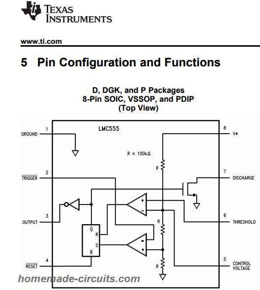
Pin Configuration:
The pinout configuration of the IC 4046 can be understood by looking at the following diagram and the below given explanation:
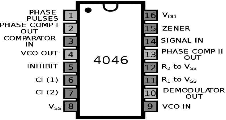
Pin#1 = PCP_OUT (phase comparator pulse output)
Pin#2 = PC1_OUT (phase comparator 1 output)
Pin#3 = COMP_IN (comparator input)
Pin#4 = VCO_OUT (VCO output)
Pin#5 = INH (inhibit input)
Pin#6 = C1A (capacitor C1 connection A)
Pin#7 = C1B (capacitor C1 connection B)
Pin#8 = VSS (ground supply voltage)
Pin#9 = VCO_IN (VCO input)
Pin#10 = SF_OUT (source-follower output)
Pin#11 = R1 (resistor R1 connection)
Pin#12 = R2 (resistor R2 connection)
Pin#13 = PC2_OUT (phase comparator 2 output)
Pin#14 = SIG_IN (signal input)
Pin#15 = ZENER (Zener diode input for regulated supply)
Pin#16 = VDD (+supply voltage)
How the IC 4046 Works
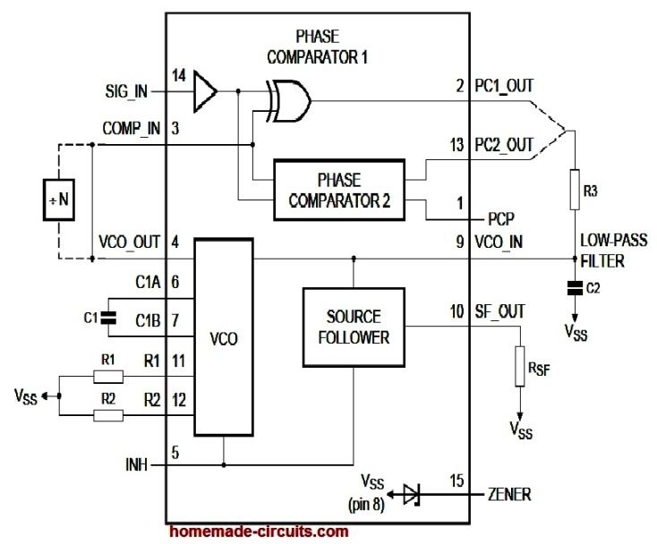
Referring to the internal diagram of the IC and the pinouts we can understand the basic working of the IC 4046 through the following explanation.
The phase detector detects the phase input. The detected output is fed to a VCO which is a voltage controlled oscillator. This creates a feedback loop across the phase detector output and VCO.
The feedback from the phase detector output causes the VCO to adjust the input phase and frequency, so that the output is phase locked and the output phase is always perfectly synchronized with the input phase.
There are a couple of phase comparator in the IC, I will try to explain one of these phase comparators.
There is also a VCO or voltage controlled oscillator inside the IC 4046. he VCO has an externally connected capacitor and resistors, which sets the center frequency for the VCO output. This sets up the VCO oscillator.
The VCO has an input voltage pinout VCO_IN which is pin#9.
If suppose we put a potentiometer across the Vcc and ground pins of the IC, and connect the wiper of the pot to the above pin#9 then we can change the VCO output frequency proportionately by changing the potentiometer adjustments.
So basically, by adjusting the voltage at the input of the VCO pin#9, we can adjust the VCO output frequency at pin#4.
Now, I have explained how the phase detector or the phase comparators work.
The phase comparators are built using exclusive OR gates. There are two inputs to the phase comparators, namely: SIG_IN, COMP_IN.
The exclusive OR gates checks and analyzes the above two input signal waveforms and averages out the ON/OFF times of the two frequencies and creates a mean waveform across their outputs. These outputs are PC_1 out, and PC_2 out respectively.
Now, how do we generate an average potential resulting from the above two output waveform of the IC 4046?
We do this simply by adding a low pass filter across the two outputs of the comparator and the gorund.
This low pass filter is created by adding a resistor R3 and capacitor C2 between the two outputs of the comparator and ground line.
This low pass filter will analyze the corrected ON time and OFF time across PC_1 and PC_2 and will convert them into an average constant DC at the center of the RC network.
This average RC potential acquired from the outputs of the phase comparators can be fed back to the VCO so that it automatically adjusts the input signal phases according to the output phase.
There are a couple of more items included in the IC 4046 which are optional but can be sometime very useful indeed.
These are a zener diode and a MOSFET source follower.
The source follower is connected with the average DC from the RC network and this buffered by the source follower so that this potential can be used for driving an external load such as a motor or an LED.
The zener diode can be used for stabilizing an external voltage to the zener value.
Application:
- Frequency synthesizers
- Clock recovery circuits
- FM demodulators
- Phase-locked loops
- Modulators and demodulators
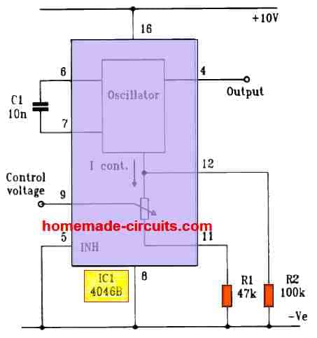
One practical application of a voltage controlled oscillator circuit using the IC 4046 can be seen in the following diagram:
Comments
Hi Swagatam :-).
I have worked for many years with communication electronics, but dimensioning PLL circuits has always been a challenge for me to set up, so I hope for help and you still are active.
I need to dimension 2 PLL circuits:
1***: A stable PLL circuit that outputs 10.7 MHz and which, ‘for example’, by via adjusting the ‘loop filter’? Gives room for FM +/- 5 kHz.
I am thinking of using something like this as a setup: (picture haves)
** Standard X-tal ‘4.096 MHz.’ together with a 74HC4060 – 74HC4046 and a 74HC40103 as a divider with only this one frequency active**.
2***: Same circuit, but without FM and that it can instead give 2 selectable frequencies: ‘10.6985 MHz. and 10.7015 MHz (for USB/LSB), via a switch.
Is this setup possible versions? (Or total out in the wood:-O.
I need to use these 2 in our project as a TX solution combined with vores ‘DDS VFO’, right now, I’m a bit stuck. ** Here is our for ‘receiver project’ for now: (Take a look)..
https://bensoe.dk/ENG_Projekt2024.html .
Hope for help.
Best 73s Jan Sørensen Denmark :-).
Hey Jan,
Thanks for the interesting question, However it seems I am unable to figure out the answer to this question, since I am not well versed with PLL circuits and ICs, the above article was written by me a long time ago, and i seem to have forgotten the working details of the IC. I hope someone else here is able to answer it for you.
Cheers!
Here is my ‘idea draft’:
https://www.homemade-circuits.com/wp-content/uploads/2025/07/4046-pll-circuit.jpg
Thanks very much for the circuit, I hope someone here will respond soon..
A standard X-tal ‘4.096 MHz.’ is not a demand, other standard X-tals you can buy are welcome.
hello, this is the Issi for the Pplons metal detector to use for sound؟Because I have a schematic chart whose voice connects to this same ISI
can you provide a complete schematic and explanation with cd4046 as pll vco to be used as an FM modulator and demodulator which functions as a plc (powerline communication) thank you.
Currently I do not have this circuit with me, If I happen to find it I will surely update it here and let you know about it..
Can you please show me the circuit of clock recovery using 4046 IC?
You can do it with any comparator, as explained in the following article:
https://www.ti.com/lit/an/sboa317a/sboa317a.pdf?ts=1717643193991&ref_url=https%253A%252F%252Fwww.google.com%252F
In 1979, the old CD4046 also helped me build a simple DSB-SC demodulator (Fc=455 KHz) without the need of I-Q signals (as in Costas Loop).
I simply added a duty cycle shaper to convert the 50% duty cycle of the limiter output (that drives the CD4046 signal input) to 25% (or 75%). I also doubled the VCO mid-frequency to 910 KHz.
This versatile AM demodulator (for m=0 to m=infinity) could be seen as a simple technique which combines Costas Loop and the Squaring Loop though with no I-Q or selective BPF (at Fc). It could be called ‘Harmonic Loop’ (since its PLL locks to the second harmonic).
Thank you for your great website. And it will be my pleasure if you also like to add this demodulator to your interesting collection (you know my email address).
Kerim Fahme (74-year-old man)
Thank you so much Kerim, for sharing your interesting experience.
I would surely like to add your demodulator circuit in the above article. If possible you can reply to this email.
Hi Swagatam. Sorry, I am not sure of which email address you are referring to by saying “If possible you can reply to this email”. In your kind reply here, there is no email address. And on this page, files cannot be uploaded (as zip). Also, if you sent me an email, I didn’t receive it yet. For instance, its schematics are drawn for LTspiceIV so that it could be simulated.
Lately, before hearing of you and your great works, I opened a topic of it titled:
“Harmonic Loop, a DSB-SC Demodulator” at the LTspice group:
https://groups.io/g/LTspice/topics?p=recentpostdate%2Fsticky,,,20,2,0,80973117
And I uploaded its LTspice files (for version 1,2,5 and 6) at
https://groups.io/g/LTspice/files/Temp/Harmonic%20Loop,%20a%20DSB-SC%20Demodulator
Although its basic version works very well (I used it for many years in my short-range RF links in the 80’s), there is always the possibility to update a circuit to make it better in some respects (for example, its ICs are very old) or make it suitable for other applications.
Hi Kerim,
When I reply to a comment on this blog, an email notification is sent to the user.
I am sure you must have also received a notification email in response to my comment replies. So I was rereferring to those emails which is sent automatically to your email ID.
However, no problem, since you have uploaded the results in those links, it will be very helpful for all the other readers visiting this page.
I appreciate your interest and experience in the field of electronics.
Hi Swagatam,
As you said, I was expecting a notification email from you. Unfortunately, I didn’t get one in my inbox or in the spam folder. Perhaps I will receive it later.
For instance, after FCC, in general, decided to provide licenses for SSB only,
there is no more reason for the today’s radio amateurs, for example, to be
interested in demodulating DSB-SC (or DSB).
But I think you know that students graduated from any faculty in data communications were told that the only practical techniques for DSB-SC demodulation are of Costas Loop and the Squaring Loop. So, I just wonder when, in the future, the professors in communications at the universities will also hear of this technique which combines the two known ones to make the demodulator’s circuit simpler (more practical).
Thank you Kerim,
I just now checked the notification system by posting and replying to a dummy comment on this site, and i could get an email notification successfully in my email inbox, so i am not sure why it is not working for you.
Unfortunately, i am not so well versed regarding the subject you are discussing, so I find it difficult to provide my opinion on this.
May I ask you a personal question? Are you also allowed knowing my email address by which I join your site? If you can know it and you will email me (since the automatic process doesn’t work in my case), I can send you the various schematics of this demodulator, ‘Harmonic Loop’, whose topology is well below your professional skills in electronics. And we will also be able to talk about it till you can publish your own article about it (as it is yours). Yes, me too, I don’t expect a return when I can help. But I don’t have the talent in presenting ideas and solutions in electronics as good as you do. But I also understand if what I propose cannot be done, for one reason or another. Anyway, thank you for your continuous care.
Thank you Kerim, I will provide you my email ID, if possible please feel free to send it in the following email, I will check them out:
homemadecircuits
@gmail.com
Thank you. When I email you the schematics, I will also notify you here.
Sure, no problem.
I got now from MAILER-DAEMON@yahoo.com
“Sorry, we were unable to deliver your message to the following address (your address). This message was blocked because its content presents a potential security issue.
I attached to my email letter 4 screenshots (by Windows 7):
[1] DSB-SC_demodulator_IF_ver2a_asc.png is the LTspice schematic of the main circuit.
[2] 455KHz_doubler.png is the schematic of the ‘455KHz Doubler’ circuit at the PLL signal input (that replaced DutyShaperIF_1).
[3] DutyShaperIF_1.png is the schematic of the original circuit at the PLL signal input (it also works).
[4] DSB-SC_demodulator_IF_ver2a_plt.png is the traces that LTspice plots when the demodulator is simulated.
I also attached, ‘DSB-SC_demodulator_455K_ver2a.zip’ which is its LTspice files in case you may use LTspice to simulate it.
The warning said that the potential security issue was found in the photo [1], DSB-SC_demodulator_IF_ver2a_asc.png!
This is the first time I heard that a ‘png’ file (a screenshot) could present a potential security issue!
I will try to resend the email and the 4 screenshots will be attached in one ‘zip’ file. Hope it will work.
Thank you Kerim,
Not sure why yahoo is not allowing those attachments to be sent. Hope this time it will be sent.
Hi Swagatam,
I got your short reply. But no matter how I tried to send you an email with an attachment (even one zip file), I got the same notice that the attachment presents a potential security issue!
It seems that, for a reason (that we both don’t know), you and I are supposed to communicate by using words only. At least, the world is kind to let us be free to talk to each other (here or via email). This is much better than no communication at all.
Best wishes,
Kerim
Thank you Kerim,
I am sorry to hear that. But no problem, you can feel free to continue sharing your ideas and suggestion in this comment section. This platform is better since it allows other readers also to find and read our discussions.