For any electronic enthusiast making PCBs for an electronic project can be a lot of fun. A printed circuit board or PCB not only helps to build compact circuit projects, it also guarantees the working of the circuit fail proof and more accurate.
In this post I will comprehensively explain a step wise process of making small DIY PCBs at home through minimum effort and maximum precision.
DIY Step-wise Procedures
It basically involves the following crucial steps:
- Cutting copper clad laminate into proper size.
- Punching indentations for drilling holes for the component leads, as per the schematic.
- Drawing pads around the indentations with etch resist paint, and linking the pads through tracks using etch resist paint.
- Immersing the painted board in ferric chloride solution, until the chemical eats away the exposed copper, leaving the painted layout sections intact.
- Drying the board and scrubbing out the etch resist paint from the tracks and the pads.
- Drilling holes on the indentations.
- Polishing the finished board with fine emery paper.
- Using the ready PCB for assembly and soldering the parts.
Now let's discuss the above steps in details. The first step in PCB production would be to acquire the essential resources and items. We are going to focus on all those things that are fundamental.
Materials Needed for Making PCB
To start the process we will first gather all the vital ingredients or materials required for the PCB making. The following fundamental things will be needed for the production
- Copper Clad Laminate
- Ferric Chloride Solution
- Etch Resist Chemical or paint.
- Painting brush or Pen
- Container for etching the PCB
- Drill Machine and Drill Bit.
- Etchant Remover
- Scouring pad, Kitchen Paper
Copper Clad Laminate
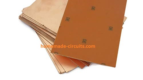
The most basic item will be the copper clad for making the printed circuit board alone, and you will find a variety of these.
The base (insulating) stuff is generally either fibreglass or SRBP (sheet resin bonded paper), and the latter is usually the more affordable option.
However, fibreglass has become the widely used both with commercial and recreational consumers as it is equipped with a couple of positive aspects.
The first is basically that it is tougher and for that reason less susceptible to bending and breaking than SRBP. The improved durability is additionally very helpful for boards that bear weighty parts for example transformers.
An additional benefit is that fibreglass is translucent and thus typically allows us to view the copper paths through the top (component) area of the board which is often worthwhile when examining and fault-finding.
Having said that, the standard of SRBP boards is more than satisfactory for many requirements. Marketing campaigns usually make reference to board as 1mm, 1.6mm, etc., and this is actually refering to the thickness of the base material.
Board Thickness
Naturally the thicker (about 1.6 to 2mm) boards tend to be more robust compared to slimmer (about 1mm) models, however the heavier quality boards are only crucial for large PCBs, or where weighty parts will likely be installed on the board.
For the majority of applications the thickness of the board is actually of little consequence.
Occasionally copper laminate board will likely be chosen as one ounce quality, or possibly two ounce quality, which appertains to the weight of the copper on one square foot of board.
Most circuits deal with just quite low currents, and regular one ounce board is just about all that's needed. In reality one ounce board is frequently satisfactory even for circuits involving formidable currents.
The Etch Resist Paint
The fundamental method by which a printed circuit board is manufactured is usually to cover the regions of copper that are necessary on the completed board through an etch resist, and after that dip the board in etchant that takes away the undesired (uncovered) regions of copper.
The etch resist is subsequently taken off to expose the copper tracks and pads.
Whichever paint that is able to keep the etchant away from the copper layout during the etching process can be employed as the resist.

I personally prefer using nail enamels or nail polish, any cheap brand can be used and will work great as an etch resist.
Properties of Etch Resist
Professionally, probably the most widely used resists are waterproof paints and inks. Water soluble varieties are definitely not fit for purpose simply because these an get dissolved and washed off in the etching solution.
A paint or ink that dries quickly is more advantageous because it eliminates the need to wait for a long time before the board could be etched.
Even the more basic printed circuit patterns appear to have a large quantity of thin copper tracks within a relatively compact area of board nowadays, and a paint brush competent at creating extremely fine lines becomes necessary.
Drawing the Track Layout
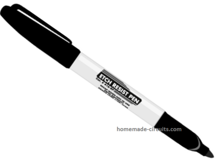
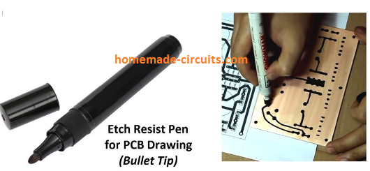
A simple solution would be to utilize an worn-out fibre-tip pen in paint brush manner, which can help develop outstanding final results although it might not look like quite a exquisite means to fix the issue. An easier way of implementing the resist is to use one of the commercially available etch resist pens which can be easily bought from any electronic part dealer.
Any kind of pen that uses a spirit based ink and a sharp point should be workable with this application. In case you are uncertain regarding the appropriateness of a pen you can easily pull out a few traces over a discarded copper laminate board then etch the board to verify if the ink maintains the etchant away correctly.
An additional type of resist are the rub-down etch resistant transfers which are available from several component merchants and which often can provide truly outstanding and specialized outcomes as demonstrated in the following example.
Actually you may find that there are lots of chemicals that can be applied as the etchant, but the majority of these are hazardous for some reason or another and are not likely suited to home designed boards.
The Etchant
The etchant is a chemical which reacts with the exposed copper area of the copper laminate and breaks it down from the board. It is used for taking off the copper regions on the board which are not painted by the etch resist and the areas which do not contribute to the track layouts and pads.

The etchant typically employed for home developed boards is ferric chloride, and while this is less hazardous compared to the majority of the choices, it is nevertheless a chemical that needs to be implemented with caution.
This should hence always be rinsed off quickly with running tap water in case you spill any on your skin. Make sure you don't store ferric chloride in metallic containers, since this chemical is reactive to metals and make the metal porous and cause leakages.
As ferric chloride is toxic (and in in the course of many uses progressively gets transformed into copper chloride which is likewise extremely poisonous) it must obviously be stored far from foodstuff and utensils etc.
Types of Ferric Chloride
Ferric chloride can be obtained in a range of different forms. Probably the most handy type to have is a ready to use solution of the chemical. Many component suppliers market it in such liquid form; typically in 250ml containers and in a concentrated form.
You must dilute it a bit prior to use, as per the given guideline on the bottle. It may not require a great deal of dilution, and a 250ml bottle normally allows only 500ml or a litre after diluting it with water.

Some companies may provide the ferric chloride as crystals, also known as "Ferric Chloride Rock" sometimes. This label is very suitable since in this form it certainly looks like pieces of yellow rock rather then tiny nice crystals, which is pretty much rock solid.
In this type ferric chloride is normally available in 500gm packages, which is enough to generate one litre of etching solution.
You can as well get this in bigger packages, but since 500gm is enough to etch a seriously great number of regular size boards and may easily survive even an diligent constructor a very long time it is most likely not rewarding getting bigger than 500gm pack altogether.
How to Create Ferric Chloride Solution
In crystaline condition ferric chloride is not going to dissolve easily in particular, however when it is stirred steadily it may sooner or later break down completely, and with constant mixing it may melt fairly quickly.
Last but not least, ferric chloride can be acquired in anhydrous form, which basically signifies it's genuine ferric chloride with virtually no water material. It will possess a slight degree of water in its crystalline form as an aside.
What actually causes this type of ferric chloride so hard to work with is the heating effect that is generated when it is mixed with water. Even if you begin with cooled water it can quickly become quite hot to a level at which the container turns very warm to touch, posing a danger of melting for plastic containers.
One more concern is that of having the chemical to dissolve adequately and create a decent etching formulation. For whatever reason you may find yourself ending up with a large quantity of chemical that will never break down, and also solution which appears like ferric chloride but has very little if any etching potential.
That is why cool water (ideally refrigerated or with ice) must be employed. It is additionally possible that there might be a tiny amount of chemical that won't melt, which can either be strained from the liquid, or as it does not appear to impede etching it could simply be left in the solution.
Drill Bit Size
The next important ingredient for manufacturing PCB at home is the drill bit, which is required for drilling holes on the PCB for the component leads.
The typical diameter for component lead holes is 1mm, though a number of components like preset resistors, big electrolytic capacitors, etc. demand a bit bigger diameter. A hole diameter of about 1.4mm is appropriate for these kinds of components.
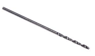
Typically, it is recommended to use a diameter of under 1mm for semiconductors and a number of other components that have thinner leads. 0.7mm or 0.8mm appear to be acceptable diameter for these components.
In case you have access to high quality drill bits they must be pretty tough.
However drill bits of around 0.7mm to 1.4mm in diameter may be quite weak and should be handled relatively carefully.
If they are maintained with downwards straight vertical pressure it may be fine, but if the orientation is not maintained at right angles to the board a proper hole won't be created which is quite possible that the drill bit will break in two.
You have to for that reason take realistic care while drilling holes using such drill bits, and preferably the machine should be used with a adjustable stand as shown below.
We have so far discussed the key things which are necessary while making a printed circuit board, and there may be some other probabilities and ends which might be essential.
These are typically basic domestic objects though, and these will be unveiled as we advance with the etching course of action. You will find many different methods for manufacturing a printed circuit board.
Despite the fact that all of them are fundamentally the identical and the major dissimilarities are just the sequence through which the different measures along the way are performed.
We are going to hence begin by taking into consideration one approach of manufacturing a board, after which a couple of alternate techniques will be explained.
Getting Started with PCB Making
The very first step would be to check with the book or magazine where the printed circuit is presented in order to get the right dimensions of the board.
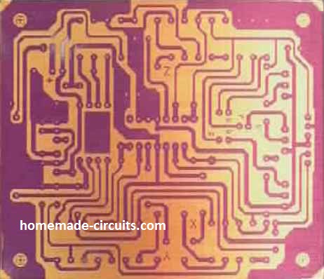
You might generally have a circuit schematic, a component overlay diagram, and the printed circuit track pattern reproduced in actual size, as given in the following 3 figures respectively.
The size of the printed circuit should be available in the text or the schematic, however in many instances it will be required to consider the proportions through the real size copper track pattern.
Mark the boundary of the finalized board on the copper side of the laminate board, then pull an additional set of lines approximately 2mm or so on the outer side of the previous marking.
By cautiously cutting between these outlines you should be able to generate a section of board with decent precision and straight edges with minimum issues.
The sides of the board could be smoothed using a small flat file, and with fibre glass board that eliminates the abrasive ends which can be undesirable.
Be aware that the markings should be done on the copper side of the board and sawn from the same side to prevent peeling of the copper while cutting the board. Therefore, make sure to cut, or drill the board always from the copper side, and not from the laminate side
The next step would be to draw the positions of the holes for the components, and wherever suitable, the fitting holes for the board mounting.
The quick method to get this done is to clamp the schematic drawing over the board on the copper track, by accurately aligning the drawing and the board edges.
Then, with a bradawl or similar pointed tool carefully and accurately marking through the schematic onto the board by punching small indentations in the copper.
It is not necessarily essential to mark the board by punching with a pointed tool, and an alternate way is to simply align and stick the drawing to the board using cello tape, and then drill down through the drawing which now itself acts like drilling markers.
Painting the Tracks with Etch Resist
After the board is trimmed to size and all holes drilled, the next task is to paint the board with the etch resist. This basically involves cleansing the board as extensively as you can.
Special cleaning blocks can be obtained from the market and these apparently perform quite nicely. Copper laminate boards may generally show some oxide and corrosion on top of the copper surface, and it is very important to remove this or else this may prevent the board from getting properly etched.
Hence, it is recommended to make use of a reasonably powerful cleaning agent which will perfectly eliminate all oxide, dirt and corrosion from the copper surface.
After the board has been comprehensively washed and the copper layer appears glistening throughout, rinse the board beneath warm water to get rid of any remnants of the cleanser or oily ingredient. At this point make sure not to touch the copper surface, which might otherwise cause greasy finger marks and slow down the etching process.
Next, take the etch resist paint to pull copper pads round the holes drilled for the components leads.
After the pads are drawn with etch resist, it's time to paint the copper tracks so that they link up the pads as per the circuit design. Always make sure to keep your hands away from the copper surface while doing this. Begin from the board one edge and proceed systematically towards the other edge, instead of doing it randomly (which might likely result in mistakes)
For Complex PCB Designs
Several contemporary printed circuit designs can be extremely sophisticated and challenging to replicate.
While designing a board of this kind it is recommended work with a printed circuit resist pen (or a appropriate alternative) with an even finer nib. In places that may have many narrow, tightly packed parallel tracks, you must take the help of a ruler to allow fine straight lines to be sketched.
If you see the tracks or pads merging with each other, wait for the resist to dry up and then make use of a compass point or other sharp pointed to scratch away the excess overlapping resist.
As soon as the resist has dried out and the PCB is inspected, the next task is to submerge the board in the etchant solution until eventually all the exposed copper has been taken off.
How PCB Etching Happens
Essentially what goes on in the course of etching is that the copper takes the place of the iron in the ferric chloride to form copper chloride, while the iron gets precipitated.
In the beginning etching process happens pretty fast and could take only a few minutes, but as the ferric chloride progressively gets transformed into copper chloride the etching action steadily becomes sluggish, and after several boards are etched it can be observed that the etching time is rather prolonged, or not getting accomplished at all.
In that case the etchant will need to replaced with new batch of ferric chloride solution. As you will notice that Ferric chloride has a red-yellow color while copper chloride is blue in color, so when you find the etching solution slowly getting towards more greenish, will indicate that the chemical is nearing the finish of its working life.
While etching the board at home in a small dish make sure the copper side of the board is facing up and the process is carried out in a non-metallic dish having adequate size.
You may want to add a decent cover on top and periodically remove the cover to check the outcome until etching is over. A main problem with this method is that an iron and copper chloride layer tends to develop on top of the board which may significantly prolong the etching time. This may be countered by carefully rocking the dish from time to time to displace off this layer so that the etching speeds up.
Using Special Containers for Etching
You may actually find it rather easy to set up a container in order to enable the PCB close to a vertical position with the copper side of the board facing downwards.
In this situation etching process happens really fast since iron precipitate is unable to develop a layer and tends to fall downwards away from the board. This ensures that the etching is not hampered. Still , periodic agitation of the board and etchant can help to knock off any small suppressing coating that may develop, enabling even faster etching.
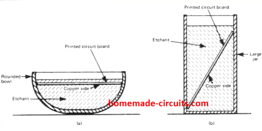
Figure above shows a few easy options for accomplishing this. In Figure (a) a curved dish is employed which ensures that the board is maintained in place through the four corners, and does not come in contact with the dish at any other points.
The technique demonstrated in (b) a good choice for bigger PCBs which may necessitate a rather huge dish to enable the procedure. The container has to be pretty sizeable, anything similar to a classic instant coffee jar would work.
A great deal of etchant will probably be required so as to practically fill up the jar. This might look a bit pricey at first, however the etchant will certainly last proportionately more time compared to a smaller quantity.
Alternatively, a lesser amount of etchant can be diluted with higher amount of water, but this could considerably decelerate etching and is not advisable.
For substantially large boards the only functional method of etching the board could be to employ a big flat dish (like a photographic dish) with the copper side facing upwards. Frequent agitation may be accustomed to speed up the etching time.
Etching will be seen happening faster on areas of where there are smaller regions of open copper, and will take a lot longer on areas of the board where there are relatively wider areas of open copper. Etching also takes place more quickly round the perimeters of the board.
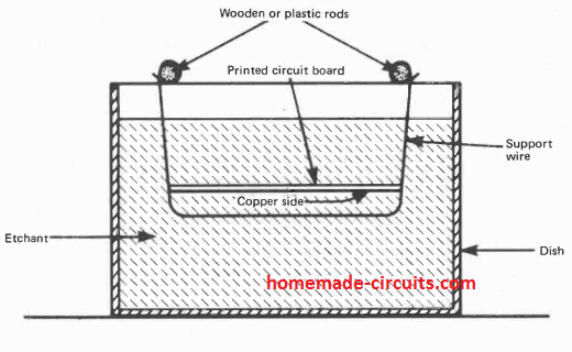
A method which usually works more effectively and is typically far easier in practice is displayed above. Here a pair of wooden or plastic rods are put down the entire length of the dish, on opposite sides. These are relatively longer than the dish to allow them to rest on top. The board is then hung from the rods supported on a couple of wire pieces, one at each end of the board.
Just a single wire is demonstrated in Figure for better understanding. If copper wire is used make sure it is a super Enameled copper wire having a thickness of 18 SWG. The wires are attached to the rods simply by turning the ends round the diameter of the rod once or twice.
After Etching is Over
When etching appears to be complete, you must thoroughly examine the board to make sure that there are no pockets of open copper left, and look for parts of the board where the copper tracks and pads are closely drawn (for example groupings of IC pads).
After you have confirmed that etching is totally accomplished, keep the board vertically over the etching solution for some moments to allow the dripping etchant elope the board, and then wipe the board using a piece of tissue paper or rag.
As an aside, this is a wise decision to maintain a piece of kitchen paper nearby throughout the etching process to ensure that remnants of etching solution could be wiped from the tweezers or gloves whenever needed. The board must be then carefully washed in water to launder away any final leftover traces of etching solution.
Removing the Resist
Finally at the end, the resist sticking on the copper has to be eliminated, that might otherwise seriously impede the soldering process on the copper pads. You can acquire any standard resist remover, and this may be in the form of a light spirit that will break down the majority of paints and inks.
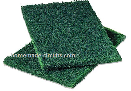
It may be also feasible to obtain printed circuit polishing blocks that happen to be likewise well suited for scrubbing of the resist. One more technique is to try using a scouring pad or powder, and this is basically among the most straightforward activities of printed circuit production which should certainly not present any kind of challenges.
To enable the final assembly of the components on the ready PCB with perfect soldering and absolutely no "dry" joints, the copper tracks and pads must be polished to a glossy finishing before the soldering of the components can be actually commenced.
Over to You
As explained above, apparently making PCB at home looks pretty simple, and it is just a matter of a few hours to create outstanding professional grade PCBs using ready made DIY materials from the market. That said, the process may require some caution and precision for achieving the desired results, so that the intended circuit project is accomplished successfully.
If you have any doubts regarding the topic, please let us now through the comments below, we'll be most happy to help!


Comments
I have found paper that is made to dissolve in water on the net – quite easy to source and not costly
laser print the PCB pattern on to the paper
Spray the clean copper board
Glue
put together and iron on with heat so its properly on and cures fast
wash the paper off in water
a light wipe with its solvent to take exposed glue on the Copper go
use the laser polyester as a solvent shield as nothing dissolves it
etch
the right glue may be found with experimentation
it needs experimenting as using water soluble and oil soluble processes is good too
a simple glue with a easy to source with light solvent
a heat to melt glue like animal glue may be good
contact adhesive the solvent costs too much
not water based PVA but oil based
not 2 pot
Thanks for the valuable info, appreciate it.
I found a new and better way, A cheap laser printer mostly prints with polyester plastic, what is not understood is polyester needs to use a alkaline based solvent and even strong water based alkaline products can be useful. Acetone is more acid in nature but Propylene carbonate is nearly related with Lithium battery’s and a little safer to use but still needs to be careful with it.
So print your PCB out on a cheap laser printer, clean the copper, setup the PCB to the paper, cover the paper with Propylene carbonate and lay the print of the laser on the copper of the PCB and do not move. Its best to be out side and use an electric steam Iron to heat and press the Propylene carbonate onto the PCB to remove the Propylene carbonate and to set laser print onto the PCB. This is very hot on the hands so use rags….. Make sure all the Propylene carbonate has gone and then boil all the paper off in a pot and rub lightly. Ready to etch.
Thank you very much for this valuable information.
I think i need to take this comment with Propylene carbonate back as I do not think it is strong enough. I believe the problem is the polyester plastic is just too difficult to desolive.
I think the better option is to use a vinyl cutter for signs their are many solvents for vinyl as they also get hot pressed on shirts too.
Its just I understand some chemistry and interested in this subject my self and seen some of the tools of others as this is the last piece and the use of hydrocarbon based with water based is so good. happy projects with cost effective ways to do PCB’s for every one
Thanks for your updates on the subject.
Your projects are very interesting to assemble but I am unable to get the talior made pcb’s.follows
request you if you can arrange to make it on payment basis so that its practical to really have them working,
from kolkata india,
Thank you, and glad you liked the post, however, we don’t sell PCBs at the moment, so can’t help much in this regards.
Great article! I have truly enjoyed your postings and projects.
Thank You!
Hello swag,
How are you. I hope you are well. Would You like to guide me for configuring constraint manager in orcad.
Basically i would like to know which option i have to select in constraint manager for track width modification,spacing between through hole component,IC,SMD IC & SMD Component.Plz give me general guideline.
Thank you.
Hello Devendra, I am good thank you…however, sorry, I am not so well versed with Orcad, so won’t be to help you in this regard.
Ok no issue. would you like to guide me for drawing pcb layout of home made solar inverter ckt. i.e. where do place active and passive component.Also plz share universal ipc standards documentation for spacing components.Both Through hole component And smd component. I want to make solar inverter PCB for learning purpose. Plz swag guide me.
Hi Devendra, Sorry, I do not have the details of the information that you have asked. If I happen to find it, I will surely update it in this site through a new post
Hello Swagatam,
Thanks for this wonderful tutorial. Though I have been here a few times (Solar Panels), I never searched for this PCB Design thing and learned most of it (probably wrongly as well) via YouTube.
You mention on your bio that you do PCB manufacturing as well. I have been doing some during the lockdown as I am no expert and these PCBs have been mostly from YouTube videos. As you can guess, they are very small in size(dimensions) and I use a Hand Tool Drill – the one where you punch by pressing because I am not a professional.
Now, I have got two larger PCB designs from an Internet friend and a YouTuber. But sadly, they are larger in size and due to the lack of my knowledge, I cannot get them done. Both are double sided as well.
Can you help me in getting those converted into workable PCBs? Please feel free to reach me detailing your pricing etc.
Stay Safe and keep giving us quality content.
Sid.
Hello Sid, I can understand your concern, however presently I am not into the PCB making job, therefore providing you with the necessary help may not be possible for me at this moment, although I wish I could solve it for you…
Hello Swagatam,
Thanks for your quick reply, very much appreciated. In fact, after posting my comment, when I wend through the others’, I did read that, no problems, I do understand. Let me risk some more money and time in trying to make one.
Just one more question – if the print on the Copper does not come out right, can I use just the thinner (or nail-polish remover) to clear the plate and retry?
Thanks Sid, Yes you can remove the layout with thinner and draw it again using enamel paint or pen.
Hi. I am 64 years old and just starting out in trying to modernise my small 4′ x 2′ N gauge model train layout. My wish is to use PWM for low speed (true to scale) operation of my 12v DC system. My issues include the 3A PWM motor speed controller DC 6v – 28v adjustable voltage regulator switches work for a day or two, then I lose the ability to control the operation via the potentiometer. All I get is full speed in forward and reverse. I know sweet FA about electronics, so basically there are a number of questions:
1. What might be the cause of this loss of control?
2. Is there a way I can add a ‘fuse’ (?) to prevent this from happening to my last two controllers?
3. Do you have a circuit on your site that will allow me to make my own ‘super PWM’ controller?
Thanks for taking the time to at least read this. Hoping to hear from you some time in the future.
Cheers
Randy
Hi, yes I have a good pwm circuit suitable for your application. You cab find it in this article:
3 Simple DC Motor Speed Controller Circuits Explained
2 Simple Bidirectional Motor Controller Circuits Explored
The problem could be due to the pot wearing out due to excessive use…
A fuse might not be relevant to the mentioned issue…this could be remedied with a digital pot or press button control.
Thanks for the quick response. A couple more questions, if I may:
Which of the 5 controllers would be the best for the operation of my model railroad?
If a loco was to derail, would a short circuit be a problem with the chosen controller?
Is there any need to alter the components listed? Will they be OK for 12-14v operations?
Thanks
You can use the second using single IC 555. To avoid short-circuit your power supply must have a built-in current controller, or you can install one between the power supply and the pwm circuit
Sir, for the PCB design, can I firstly use pencil to draw the circuit diagram on the copper clad laminate board and later use etch resist pen to trace the circuit diagram on the copper board? And if yes, how would I determine the dimension of each component drawing on the copper board?
Hi OGUNFESOLA, Drawing on the PCB can make things complex. You should draw on paper first, then fix the paper over the board, punch the drilling pad points using a pointed metal, and then draw the pads and the connecting tracks with etch paint. The component dimensions must be determined on the paper itself.
Thanks sir
Dear Swagatam,
Thanks for your updates on the subject.
Your projects are very interesting to assemble but I am unable to get the talior made pcb’s.
request you if you can arrange to make it on payment basis so that its practical to really have them working.
Thank you Dear Mohan, Unfortunately I do not have any PCB maker in my contact list at the present moment, around 5 years ago I used to be in contact with a few of them but in the course of time I lost all the details.
you’re a genius! start placing amazon or any other partner links for parts used so its easier for people to source parts and you get a kickback from the sale
Thanks Shekhar, for the suggestions, If feasible I will try that!
Hello Swag thank you for pcb manufacturing link. Its a great and useful study Material.
Would you like to guide me for pcb designim using any software tool Like Orcad , Eagle. To design a pcb what are the thumb rules for schematic , layout preparation,routing,tracs, creepage And clearances,selection of pads etc.
Thank you
Thank you Devendra, Since I am not an PCB expert so advising the most appropriate techniques and softwares may not be possible for me. However, the basic rules that apply universally to PCB designing are as follows.
Keep sufficient distance between the tracks so that no accidental shorting occurs, calculate track thickness as per the amount of current it’s supposed to handle. Do not make sharp turns with sharp edges on the tracks. Try to estimate the most efficient track positioning to avoid unnecessary long looping tracks. For RF circuits make sure to employ ground plane technique, meaning having the entire PcB covered with grounded copper base, and the internal connecting tracks etched in between this ground plane copper base. The pad size must eb according to the component lead size. it can be generally a 2mm diameter, can be smaller than this if the PCB demands it, except for 1N4007 diodes.
A very useful and easily understandable material. Thanks for your great initiative
Thanks, glad to help!