The main technical function of the proposed voltage regulator is voltage stabilization. It is capable of stabilizing an input voltage ranging from 0 to 600 Vdc to an output voltage ranging from 100 to 560 Vdc, with a maximum current of 800 mAdc and maximum power dissipation of 100 W. The unit also exhibits good stability, with a stability of less than 0.1% after 15 minutes of constant input voltage, and a rejection of input ripple greater than 60 dB. By Atul Shah
Often relegated to the status of a neglected or poorly studied 'add-on component' due to lack of interest, the power supply of an electronic circuit can be a source of many disappointments. The following article reminds us of some fundamental points and proposes the designing of a versatile 600 Vdc high voltage regulator module.
The main characteristics of a power supply are the required 'voltage' and 'power', internal stability under variable load, drift over time, and noise rejection.
Power supply
The voltage and current data are quickly fixed according to the demand of the circuit. The internal impedance, on which load stability, time stability, and noise rejection depend, is often a characteristic suffered by the circuit design.
For example, a 30W class AB2 stereo tube amplifier can easily see its current vary between 100mA and 400mA. The high voltage, rectified and filtered by a "choke" coil, will see its voltage drop by several tens of volts, especially if rectified using a valve.
This means that the power supply collapses at the moment when your amplifier needs it the most! The internal resistance of a power supply represents a major key, especially as the voltage is higher.
Any passionate amateur has already experienced its effects, such as "motor boating," an oscillation that results in a slow pulsation that sounds like a boat motor noise in the speakers.
This instability is mainly caused by the power supply's internal resistance being too high.
Note also that this phenomenon is influenced by too much feedback and circuits that go too "low" in frequency.
Our study Regularly confronted with the problems described above, we have developed a high-voltage stabilizer module based on the circuit that we use in many of our projects.
With small dimensions (80 x 40 mm), it fits into most designs. Furthermore, it allows for the elimination of the cumbersome filtering choke. It can be used for the universal stabilization of any voltage between 100Vdc and 600Vdc.
Circuit Description
The 600V regulator circuit module is inserted between the ballast capacitor and the load as shown below.
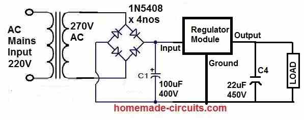
Rectification and electrolytic capacitors are external. Only four connections are required: the input and its return, the output, and its return. The two returns are connected to the floating ground of the module.
The voltage stabilization is achieved at the collector of Q1. The 10.7 V present at the two zener diode terminals biases the emitter of the PNP transistor to 10V, and a stable current of 1mA flows through resistor R2 of 10kΩ. This same current develops a stable voltage across resistors R3, R4, and P1 at the collector.
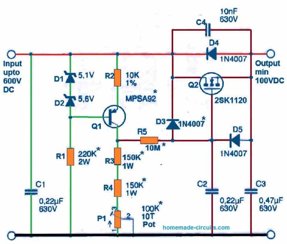
This voltage is filtered by the R5-C2 filter and biases the gate of the MOS transistor/Q2. The output voltage is taken from the "source" of Q2.
Note that the Vce voltage of Q1 can vary considerably. In fact, the input voltage is not filtered and can have a ripple of several tens of volts. Additionally, this voltage varies according to the vagaries of the sector and the variations in the output load current.
The voltages indicated on the diagram are those expected for an input voltage of 380V to 450V and a stable output voltage between 300V and 400V.
As the module accepts many other values, here are some indications to define certain components. The values of D1, D2, and R2 are invariable. The capacitor values are not critical as long as the same orders of magnitude and service voltages are respected.
Components marked with an asterisk can be changed according to needs. First of all, to ensure proper stabilization, it is imperative to maintain an input voltage that is about 20 volts higher than the output voltage. R1 must impose a current of 2mA to 3mA in the zener diodes.
Resistors R3, R4, and potentiometer P1 are calculated to develop the desired voltage based on the 1mA current that flows through them.
The PNP/Q1 transistor is an MPSA92 that supports 300V.
It can be replaced by a 2N5401 if Vce does not exceed 150 V. The R5-C2 filter allows for a 70 dB rejection of the ripple at 100 Hz, but the high voltage takes about twenty seconds to settle. By replacing R5 with a value of 1 MSS, the voltage settles immediately and the ripple rejection is still 50 dB.
It should be noted that with a typical choke, the attenuation of residual ripple is about 20 dB. Additionally, the choke adds a resistance of several tens of ohms to the internal resistance of the power supply.
Finally, the chosen transistor Q2 is a 2SK1120 from Toshiba. We chose this one because our BUZ305 became unavailable.
The 2SK1120's TO-247 package has two advantages:
- The length of the leads is 20 mm (15 mm for the BUZ305)
- The top surface and the mounting hole are insulated, eliminating the need for an insulating sleeve.
However, it is possible to replace it with a 2SK1489 with a maximum power dissipation of 200 W.
The regulator circuit module operates from an input voltage of around a hundred volts that can be raised to a maximum of 600 Vdc. It must deliver a minimum current of 20 mA and can easily reach 1 A, provided that the MOSFET's dissipation limits are respected.
Heatsink Specifications
The heat sink also has a thermal resistance with respect to ambient air, which can be reduced to very low values by using a fan. These thermal resistances must be taken into account as they cause a shift in the graph towards lower values.
Practical example: suppose the ballast transistor consumes 30 W, is insulated by a 0.85°C/W spacer, and is mounted on a 1°C/W heat sink. The heat sink removes the heat, and the temperature rise will be 30°C, plus the 25°C ambient temperature, totaling 55°C.
The transistor temperature will be even higher, by 25.5°C (30 x 0.85), due to the thermal resistance of the spacer, making it 80.5°C. This is still within the safe range, as the maximum allowable dissipation at 85°C is still 80 W.
Different mechanical mounting configurations have been provided. The first is mounting on an aluminum block of 40 x 80 x 6 mm with a spacer for integration into a closed chassis. If the aluminum block is screwed onto the chassis or an external heat sink, the module can dissipate up to 40 watts, which is more than enough for most audio applications.
The second possibility is external mounting. For this purpose, the module is placed on an aluminum base of 84 x 70 x 5 mm, fixed to the chassis, and protected by a transformer cover of type E184. The allowable dissipation is also around 40 watts.
The third option involves mounting the transistor without a spacer. The electrical insulation will be between the aluminum block at the input HT potential and the heat sink.
The thermal interface is located between the 40 x 80 mm aluminum block, which has an area of 32 cm², and the heat sink.
The thermal resistance of the insulation will be around 0.08°C/W. With a fan-assisted heat sink, it is possible to dissipate 120 watts, which is mainly applicable for laboratory power supplies.
Use & Technical Specifications
This 600V high voltage circuit module integrates all the essential elements for stabilization and can be mounted far from the voltage source and its use.
All tests have been carried out with 50 cm leads between the ballast capacitor and the module, as well as between the module and the loads, without any instability problems. The module's own internal resistance is around 5 Ω at constant input voltage.
However, this resistance is influenced by the transformer's power. For our test, we use a 110 VA transformer, a bridge rectifier, and a 100 pF buffer capacitor. The internal resistance of the entire setup is then established at 13 Ω.
When integrating the module into a design, it is advisable, in the first instance, to protect the module with a quick fuse and a hundred ohms resistor to ensure that the output current is limited to an acceptable value.
With such a low internal resistance, any short circuit in the output line will be fatal to the ballast. The stability of the output voltage is measured by varying the input voltage. A variation of 330 Vdc to 400 Vdc at the buffer capacitor, equivalent to a ±10% mains variation, produces a 2 Vdc output variation.
After stabilization for ten minutes with a constant input voltage, the output voltage remains within a range of 0.1%.
The rejection rate is the ratio between the input ripple voltage and the output voltage. For a current consumption of 200 mA, the input ripple voltage is 6 Vac, and the output ripple is 2 mVac, resulting in a ratio of 3000 or 70 dB.
The table of technical specifications shown below reflects the various possibilities in voltages and currents. We must not forget that the values of the voltages, currents, and powers are intimately linked by the relation:
(Vin - Vout) x I = P.
| Technical Characteristics | Specifications |
|---|---|
| Maximum Input Voltage (*) | 600 Vdc |
| Output Voltage (`) | 100 - 560 Vdc |
| Current (*) | 0 - 800 mAdc |
| Maximum Power Dissipation (*) | 100 W |
| Stability for Uin +/- 5% | 41-0.5% |
| Stability for constant Uin | <0.1% after 15 min |
| Ripple Rejection (*) | >60 dB |
| Residual Ripple (I=250 mAdc) | <3 mVac |
| Static Internal Resistance | <10 Ω |
| Internal Impedance | >100 Hz <10 Ω |
| Dimensions (LxWxH) | 80 x 40 x 40 mm |
| Weight | 100 g |


Comments
Dear Swagatham,
In the above circuit, the mosfet is used a source following.
The Gate-Source voltage of the said Mosfet is only +-20v
[Maximum Gate-Source Voltage |Vgs|: 20 V]
in my experiments, what I have seen is , output at source is almost equal to the gate voltage.
Can we give more than the specified Vgs voltage ? obviously we cannot get outputs like 100v without providing 100V at gate. But how ? is my understanding wrong ?
I have blown many mosfets trying to get about 80v at the source of the mosfet. I am trying to figure out why it is blowing off ?
another strange thing is with gate open , if I connect 80 v at source, it is fully available at gate, instantly damaging the mosftet. No load was connected at the drain and gate too was not connected. why this behavior ?
Your ideas are most welcome.
dear Swagatam
I understand that P1 should be 1W of power. Is Not more practical to replace it by a transistor and put a trimpot to adjust the voltage output?
Thank you Emerson, for the suggestion,
However I am not sure how a transistor circuit can be replaced with the P1 trimpot.
Hi Swagatam,
I’m trying to copy your design using an NPN transistor to replace Q1. Is there any way that I can send the schematic for your review?
Btw, may I understand the purpose of R3, R4 and P1 as the voltage divider with Q1? From my understanding, you take the output from Q1 collector. Can you explain how you use Q1 output to drive Q2 for the regulation?
Thanks and look forward to your reply!
Thank you Kevin,
The R3, R4, P1 are positioned for regulating and feeding a proper voltage for the MOSFET gate, so that it does not exceed 20 V or 25 V. Because the MOSFET gate volatge exceeds 25 V it get destroyed.
This means I can increase either the Q1 current drawing or the value of R3, R4, and P1 to make the circuit stands for even higher input voltage, correct?
For higher input voltages you will have to upgrade Q1, Q2 appropriately, and also adjust the R3, R4, P1 values appropriately.
R/Sir,
Is it possible to increase its current upto 25 amp? If possible then what changes should be required?
Regards
Avdhoot
Hello Avdhoot, Yes you can increase the current to any limit, simply by upgrading the IGBTs accordingly.
Good morning sir,
Thanks for quick response.
1. Can I use KGF25N135NDH – 1350V 75A N-Channel IGBT instead of 2SK1120?
2. Is it required to change the MPSA92 PNP High Voltage Transistor? If yes please suggest type or model name.
Thanking you Sir.
Avdhoot
Good Morning Avdhoot,
1) You can use the mentioned IGBT if your load is also rated at around 1000 V otherwise you can use an IGBT or a MOSFET whose maximum voltage capacity is not more than 100 V higher than the load voltage.
2) If you are not able to find the MPSA92 transistor, you can replace it with any 300 V 1 amp PNP transistor
Very very thankful
Ok sir I will be check igbt.
MPSA92 is available so I can use it.
Once again thanks.
No problem, let me know if you have any more questions.
R/Sir,
I have 2 more issues one is this circuit related and another is VFD related
1. For this circuit required 0.22uf 630v/ 0.47uf 630v / 10nf 630v each capacitor but I have only two type capacitor available apart from 0.22uf 630v so can I take 0.47uf 630v instead of 0.22uf 630v ? If yes then it will be 2 in parallel or a single one?
2. For VFD The H-Bridge Driver Circuit I am going to use IRS2110 03 Nos instead of IRS2330 IC and for the whole project all components are available accept 10uf/1kv capacitor. I have 47uf/250v capacitors so it is possible to replace the 47uf/250v(4 capacitors in series) with 10uf/1kv.
Apart from these two components all material is available for my both projects.
Plz advise.
Regards
Avdhoot
Hi Avdhoot,
1) You can use a 0.47uF/630V for C2 instead of 0.22uF/630V, it should work. A single one should be enough.
2) for the VFD circuit you can use 4 series connected 47uF/250V that will do the job.
All the best to you.