The IC TL494 is a versatile PWM control IC, which can be applied in many different ways in electronic circuits. In this articles I have explained in detail regarding the main functions of the IC, and also how to use it in practical circuits.
General Description
The IC TL494 is specifically designed for single chip pulse width modulation application circuits. The device is mainly created for power supply control circuits, which can be efficiently dimensioned using this IC.
The device comes with an in-built variable oscillator, a dead-time controller stage (DTC), a flip flop control for pulse-steering, a precision 5 V regulator, two error amps, and some output buffer circuits.
The error amplifiers feature a common mode voltage range from - 0.3 V to VCC - 2V.
The dead time control comparator is set with a fixed offset value for delivering a constant 5% dead time approximately.
The on chip oscillator function can be overridden by connecting the RT pin#14 of the IC with reference pin#14, and by externally providing a sawtooth signal to the CT pin#5. This facility also allows driving many TL494 ICs synchronously having different power supply rails.
The output transistors inside the chip having floating outputs are arranged to deliver either a common-emitter output or a emitter-follower output facility.
The device allows the user to get either a push-pull type or a single ended oscillation across its output pins by appropriately configuring pin#13, which is the output-control function pin.
The internal circuitry makes it impossible for any of the outputs to produce a double pulse, while the IC is wired in the push-pull function.
Pin Function and Configuration
The following diagram and explanation provide us the basic information regarding the pin function for the IC TL494.
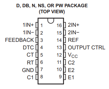
- Pin#1 and Pin#2 (1 IN+ and 1IN-) : These are the non-inverting and inverting inputs of the error amplifier (op amp 1).
- Pin#16, Pin#15 (1 IN+ and 1IN-) : As above these are the non-inverting and inverting inputs of the error amplifier (op amp 2).
- Pin#8 and Pin#11 (C1, C2): These are the outputs 1 and 2 of the IC which connect with the collectors of the respective internal transistors.
- Pin#5 (CT): This pin needs to be connected with an external capacitor for setting the oscillator frequency.
- Pin#6 (RT): This pin needs to be connected with an external resistor for setting the oscillator frequency.
- Pin#4 (DTC): It's the input of the internal op amp which controls the dead-time operation of the IC.
- Pin#9 and Pin#10 (E1 and E2): These are the outputs of the IC which connect with emitter pins of the internal transistor.
- Pin#3 (Feedback): As the name suggests, this input pin is used for integrating with an output sample signal for a desired automatic control of the system.
- Pin#7 (Ground): This pin is the ground pin of the IC, which needs to connected with the 0 V of the supply source.
- Pin#12 (VCC): This is the positive supply pin of the IC.
- Pin#13 (O/P CNTRL): This pin can be configured for enabling the output of the IC in the push-pull mode or single ended mode.
- Pin#14 (REF): This output pin provides a constant 5V output which can be used for fixing a reference voltage for the error op amps, in the comparator mode.
Absolute Maximum Ratings
- (VCC) Maximum Supply voltage not to exceed = 41 V
- (VI) Maximum Voltage on input pins not to exceed = VCC + 0.3 V
- (VO) Maximum output voltage at collector of internal transistor = 41 V
- (IO) Maximum current on Collector of the internal transistor = 250 mA
- Maximum IC pin soldering heat at 1.6 mm (1/16 inch) away from IC body not to exceed 10 seconds @ 260 °C
- Tstg Storage temperature range = –65/150 °C
Recommended Operating Conditions
The following data gives you the recommended voltages and currents that can be used for operating the IC under safe and efficient conditions:
- VCC supply: 7 V to 40 V
- VI Amplifier Input Voltage: -0.3 V to VCC - 2 V
- VO Transistor Collector Voltage = 40, Collector Current for each Transistor = 200 mA
- Current into Feedback pin: 0.3 mA
- fOSC Oscillator frequency range: 1 kHz to 300 kHz
- CT Oscillator timing capacitor value: Between 0.47 nF to 10000 nF
- RT Oscillator timing resistor value: Between 1.8 k to 500 k Ohms.
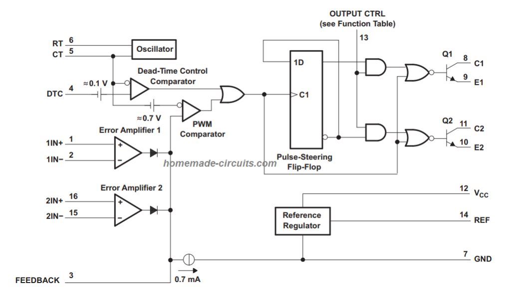
Internal Layout Diagram
How to Use IC TL494
In the following paragraphs I have explained the important functions of the IC TL494, and how to use it in PWM circuits.
Overview: The TL494 IC is designed in such a way that it not only features the important circuitry needed to control a switching power supply, but additionally tackles several fundamental difficulties and minimizes the need of supplemental circuit stages necessary in the overall structure.
The TL494 is basically a fixed-frequency pulse-width-modulation (PWM) control circuit.
The modulation function of output pulses is achieved when the internal oscillator compares its sawtooth waveform through the timing capacitor (CT) with both pairs of control signals.
The output stage is toggled in the period when the sawtooth voltage is higher than the voltage control signals.
As the control signal increases, the time when the sawtooth input is higher decreases; consequently, the output pulse length reduces.
A pulse-steering flip-flop alternately guides the modulated pulse to each of the two output transistors.
5-V Reference Regulator
The TL494 creates a 5 V internal reference which is fed to the REF pin.
This internal reference helps to develop a stable constant reference, which acts like a pre-regulator for ensuring a stable supply. This reference is then reliably used for powering various internal stages of the IC such as logic output control, flip flop pulse steering, oscillator, dead time control comparator, and PWM comparator.
Oscillator
The oscillator generates a positive sawtooth waveform for the dead-time and the PWM comparators so that these stages can analyze the various control input signals.
It's the RT and the CT which are responsible for determining the oscillator frequency and thus can be externally programmed.
The sawtooth waveform generated by the oscillator charges the external timing capacitor CT with a constant current, determined by the complementing resistor RT.
This results in the creation of a linear-ramp voltage waveform. Each time the voltage across CT reaches 3 V, the oscillator quickly discharges it, which subsequently restarts the charging cycle. The current for this charging cycle is calculated through the formula:
Icharge = 3 V / RT --------------- (1)
The period of the sawtooth waveform is given by:
T = 3 V x CT / Icharge ----------(2)
The oscillator frequency is thus determined using the formula:
fOSC = 1 / RT x CT ---------------(3)
However, this oscillator frequency will be compatible with the output frequency when the output is configured as single-ended. When configured in push-pull mode, the output frequency will be 1/2 of the oscillator frequency.
Therefore, for single ended output the above equation no 3 can be used.
For push pull application the formula will be:
f = 1 / 2(RT * CT) ------------------(4)
Dead-time Control
The dead-time pin set-up regulates the minimum dead time (off periods between the two outputs).
In this function when voltage on the DTC pin exceeds the ramp voltage from the oscillator, forces the output comparator to switch OFF the transistors Q1 and Q2.
The IC has an internally set offset level of 110 mV that guarantees a minimum dead time of around 3% when the DTC pin is connected with the ground line.
The dead time response can be increased by applying an external voltage to the DTC pin#4. This allows to have a linear control over the dead-time function from the default 3% to a maximum of 100%, through a variable input of 0 to 3.3 V.
If a full range control is used, the output can of the IC can be regulated through an external voltage without disturbing the error amplifier configurations.
The dead-time feature can be employed in situations where added control of the output duty cycle becomes necessary.
But for proper functioning it must be ensured that this input is either terminated to a voltage level or to ground and should be never left floating.
Error Amplifiers
The two error amplifiers of the IC have a high gain, and are biased through the ICs VI supply rail. This enables a common-mode range of input from -0.3 V to VI - 2 V.
Both the error amplifiers are internally set up to work like a single-ended single supply amplifiers, wherein each output have active-high capability only. Due to this capability, the amplifiers are able to activate independently for satisfying a narrowing PWM demand.
Since the outputs of the two error amps are tied like OR gates with the input node of the PWM comparator, the amplifier which can work with minimum pulse out dominates.
The amplifiers have their outputs biased with a low current sink so that the the IC output ensures maximum PWM when the error amplifiers are in the non-functional mode.
Feedback Control
The feedback control for TL494 is actually simple. The feedback affects the output PWM of the IC.
If you use the error op amps to control the feedback then the output PWM can be reduced to almost zero by applying a DC feedback from the inverter output to the non-inverting pin of the selected opamp with reference to the 5.1V applied at the inverting input of the selected opamp.
This 5.1V reference is readily available from the TL494 itself. If you want to control the PWM to some desired customized level then you can do that by applying a controlled voltage to pin#3 of the IC.
Output-Control Input
This pin of the IC can be configured to allow the IC output to either work in a single ended mode that is both output oscillating together in parallel or in push pull manner producing alternately oscillating outputs.
The output-control pin works asynchronously, enabling it to have a direct control over the output of the IC, without affecting the internal oscillator stage or the flip flop pulse-steering stage.
This pin is normally configured with a fixed parameter as per the application specifications. For example, if the IC outputs are intended to work in parallel or single ended manner, the output-control pin is connected with the ground line permanently. Due to this the pulse-steering stage inside the IC gets disabled and the alternate flip flop stops at the output pins.
Also, in this mode the pulses arriving at the dead-time control and PWM comparator are carried together by both the output transistors, allowing the output to switch ON/OFF in parallel.
For obtaining a push pull output operation, the output-control pin simply needs to be connected to the +5V output reference pin (REF) of the IC. In this condition, each of the output transistors turn ON alternately through the pulse-steering flip-flop stage.
Output Transistors
As can be seen the second diagram from top, the chip consists of two output transistors, which having uncommitted emitter and collector terminals.
Both these floating terminals are rated to sink (take in) or source (give out) up to 200 mA current.
The saturation point of the transistors is less than 1.3 V when configured in the common-emitter mode, and less than 2.5 V in the common-collector mode.
They are internally protected from short circuit and over current.
Application Circuits
As explained in the above, the TL494 is primarily a PWM controller IC, therefore the main application circuits are mostly PWM based circuits.
A couple of example circuits are discussed below, which can be modified in various ways as per individual requirements.
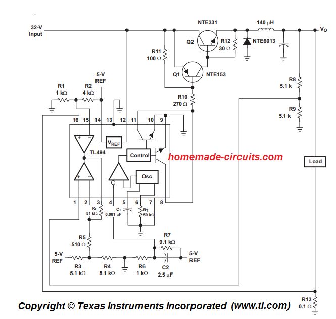
Solar Charger using TL494
The following design shows how the TL494 can be effectively configured to create a 5-V/10-A switching buck power supply.
In this configuration the output works in parallel mode, and therefore we can see the output-control pin#13 is connected to ground.
The two error amps are also used very efficiently here. One error amplifier controls the voltage feedback via R8/R9 and keep the output constant at the desired rate (5V)
The second error amplifier is used for controlling the maximum current via R13.
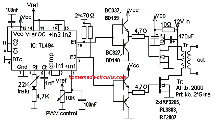
TL494 inverter
Here's a classic inverter circuit built around the IC TL494. In this example the output is configured to work in the push-pull manner, and therefore the output-control pin here is connected with the +5V reference, which is achieved from pin#14. The erst of the pins are also configured exactly as described in the above datasheet.
Conclusion
The IC TL494 is a PWM control IC with highly accurate output and feedback control facilities ensuring an ideal pulse control for any desired PWM circuit application.
It is similar to SG3525 in many ways, and can be used as an effective replacement for it, although the pin numbers can be different and not exactly compatible.
If you have any questions pertaining to this IC, please feel free to ask them through the comments below, I'll be happy to help!
Reference: TL494 datasheet


Comments
Hola Swagatam,
looks like you are experienced on magnetics, cores as well. Any hint on building a solar MPPT >> higher voltage charging solution from scratch with preferably kicad & spice?
I search for a efficiency vs complexity solution. So far i investigated buck boost topologies but thought that days about a H-bridge transformer solution. Due to the push pull from + to – Vcc on the primary side I avoid core remanenz and use a wider magnetic change.
Disadvantage so far how to adjust the output voltage which should be able with PWM D equals energy transmission?
Lot more to think about like apropiate diodes with low Ufw Ifw at Fosc, …..
First stage planning:
Pmin 500W …. 2kW with 4 solar panels & mppt per panel input
Uin_min 15Vdc … 45-50Vdc = Voc solar panel
Uout_max 57Vdc for 48V … 72V LiFePo
If answering please CC to my pm as iam not regularly around nor specifically read this artice once more. Github sourceforge … would be great
Regards
Thanks Don,
I can design this circuit for you.
I already have one similar design on this website but it is only 18V rated.
https://www.homemade-circuits.com/real-mppt-solar-charger-circuit-using-arduino-lcd-and-manual-auto-switch/
24 VOLT TO 13.5 VOLT 30AMPERE OUTPUT STEP DOWN CONVERTER CIRCUIT USING THIS IC
Satheesh, please check the second last circuit in the above article, that is exactly what you need…
Hello big man. I need the PCB circuit of the second part of the Chinese inverters that converts 310V DC voltage to AC with adjustable frequency using TL494. Do you have this PCB in your archive?
Thank you for such a detailed description of the chip. I have ZU-75Y under repair. Can’t find the diagram. There is no tension on the 12th leg. I can’t understand where it comes from.
Yes indeed pin12 must be connected to the positive supply rail…your PCB could be a double sided one, so the Vcc pin could be getting the supply from the flip side of the PCB
Hello Reza, sorry I do not have the PCB design, but I can provide you with the circuit diagram for that…
Hell Swag,
I’m curious about the transformer used in the Push-Pull converter schematic. What does
Tr:
Al kb. 2000
Pri: kb. 2*5 me
mean?
Am I correct in assuming that the core type has an AL of 2000 and primary winding of 2×5 turns?
Thanks,
DaveM
Hi Dave,
Here’s the possible explanation:
“Al kb. 2000”:
“Al” means the inductance factor of the ferrite core.
“kb. 2000” most likely means AL = 2000 nH/turn² which is a common way to express ferrite core property.
This tells how much inductance you get per turn squared.
So if you wind 1 turn:
L = AL × N² = 2000 × 1² = 2000 nH
If 5 turns:
L = 2000 × 25 = 50,000 nH or 50 µH
“Pri: kb. 2×5 me”:
“Pri” = Primary winding.
“2×5” = Two windings of 5 turns each, one for each MOSFET side in the push-pull setup.
“me” might be a shorthand for the “multi-strand enameled wire” or “magnet wire”. Some people say “me” for “multi enameled”.
So it means:
Primary = two separate 5-turn windings, maybe wound on opposite sides or bifilar style for driving through each MOSFET.
regarding the TL494, when I substitute an SMD version for through hole version, the circuit doesnt work exactly the same anymore. Is there a known performance difference between these?
thank you very much Mr. Swagatam
Actually I have been using this TL494 circuit for a long time and the pin outs are no problem. The issue is the automatic response to back EMF, which allows this DC to square wave AC inverter to handle fans, unlike simpler, pure Squarewave AC circuits. When I replace the old version DIL through hole TL494 with SMD TL494, everything is perfectly connected, and the square wave is fine, but the ability to handle a fan goes away. I suspect that the zero duty cycle adjust portion of the circuit works with the 30-35v zener to shut off a cycle when back EMF is present? but that this is slightly different with a newer TL494 SMD. I do not suspect a counterfeit because I bought the SMD from digikey. This circuit normally works with inductive loads via a response portion which seems to involve the duty cycle zero adjust when encountering an inductive back pulse.
By the way, I really like your website. I put my circuits into a book which I sell on Amazon entitled “Take Back The Power!” best regards Mots
Thank you Marvin, for the valuable information,
Your analysis about the issue could be right, and I hope you are able to solve it soon.
Thank you again for your kind words, and glad you like this website.
All the best to you, hope you get more customers for your books.
Did you confirm the pinout arrangement of the two variants in the datasheet, if they match exactly then I don’t think there should be any problems with their working, and both the versions should provide the same results?
sir this tl494 inverter and CD4047 inverter which one is more better
4047 is better if iron core transformer is used
please I’m looking for a circuit diagram push pull oscillator from 10 to 150 khz and dyty cycle from 0 to 100 % can you help me ?
You can use any IC 555 astable circuit and adjust it at the required frequency.
Dear Swagatam
What is the final output frequency at the transformer output of the tl494 inverter circuit below, that is the third diagram?
Hi Richard,
The frequency will need to be set using the 22k preset on pin#6 of the IC. You can try adjusting the preset until the output is a good 220V and the mosfets not heating up.
hi swagatham.how do you disable the protection circuit of this ic when used in a car amplifier
Hi Aldrin, I will have to see the schematic to solve the issue.
I want to make Buck converter of 48 volts to 12 volts 10amps ..please help
You can modify the following concept suitably, for the mentioned application
https://www.homemade-circuits.com/5v-pwm-solar-battery-charger-circuit/
Thank You so much for this article..!
You are welcome!
Hello Swagatam, thanks for another useful article here.
I have a query and hope you can help me out. How can I change or set the output voltage of the first circuit (or any circuit utilizing the TL494 PWM chip) to something different, like 12V or 18V? Which components should I change/modify to achieve an output voltage of my choice?
Thanks
Thank you Chinmoy,
You will need a boost converter topology for getting 18V from a 12V source. I have one design which you can try but it uses a TL497 instead of TL494
https://www.homemade-circuits.com/high-power-dc-to-dc-converter-circuit-12-v-to-30-v-variable/
You can try the following version using op amps
https://www.homemade-circuits.com/12-v-to-19-v-converter-circuit/
I wanted to see if i can make a temperature controller with a 100k pot, 10k thermistor, tl494 to go with a relay driver i have made from an 18v mains trafo and some discreet components.
The 18v ac trafo is wired with a fwbr but also utilizes a half wave rectified subcircuit on one ac input and it ramps the voltage to about…well in certain configurations i can (very briefly!) pull over 100 watts from the mains, and can configure it to burst caps.
It incorporates a latching option in relay driver mode, tops out at about 35v dc max at very low power, and drives a dual 120v relay which has a 24v dc coil (I’m not sure of its ohms-it is from a microwave or amp-i can’t rem which).
I know i should be able to use a divider and an ntc with a transistor but it keeps bursting them (i haven’t wanted to risk the larger ones-i burnt up three mosfets with spikes on shutdown/restart before i was able to configure protection with adding a diode/cap/dual npn arrangement)…. have tried 3904/6 and small ones and they worked to control the inrush problems but I can’t get one to respond right with an ntc divider.
Cool thing is it supplies several voltage references and it has positive and negative railings to use if nesc (up to 8v dc negative away from the up to 24 v dc positive; but that 8 could always be amplified with a dc to dc boost circuit if a higher negative voltage was needed.
It also has led indicators for red and white standby and a green one which illuminates if the relay coil is active.
The inrush was hard to control…but once i did that…im sure 555 temp circuits will drive this but I wanted to use a 494 bc I am curious how it would be arranged to activate by temperature. Ultimately this relay driver needs to control a heater so the adjustability for the temp range needs to be 60-85f or so.
You could do it by voltage control too but im not anywhere near as good as you are. I make nifty accidents….you are an actual engineer.
I think you would like a video or at least a pic of the driver. The trafo was once a charger for some long destroyed cordless tool. I can make it latch, then cross the input with the same wire that latches it to unlatch it, in one configuration (takes one cap) or it just latches by full contact of the control wire.
I can also put the relay into an astable mode…but it takes another cap and resistance which I am not sure of because each time I’ve done that i was using a partially burnt led as a resistor and im not sure of the value it takes but it can be done (i didnt pursue it bc that’s not what my intent for this device, but it is interesting that it can be done).
Email me if you want me to send a pic.
I can send one of a project based on a micro control board which is nifty because it amplifies sound from a small fan which has speed control, and lights, and it runs on a standard 5v usb. It sounds like a motor…and we could attach a mic array and probably get beyond unity with it but it does use 7.7 watts at 120v ac.
-jes
Using a relay with TL494 for controlling temperature may not be applicable, because TL494 is basically an oscillator chip with a feedback control.
If your temperature control is PWM based then probably the IC’s in-built error op amps could be used for making a self adjusting temperature controller circuit using a themistor.
For making an accurate thermistor based temperature controller, you would only need an opamp comparator circuit as explained in the following example circuit (1st and the last schematics):
3 Accurate Refrigerator Thermostat Circuits – Electronic Solid-State
BJTs cannot be used for getting precise cut off points with a thermistor divider.
Thanks for your respond. So if I connect pin2 of triac bt136 to Ct pin of TL494 and pin 1 of triac bt136 to ground, pin3 of triac bt136 gets positive signal of overload or low battery. Will Ct of TL494 be grounded so that the IC shutdown?
Yes that is possible. An SCR would be more suitable such as BT169. You can first test the operation by manually shorting Ct pin to ground.
Ok. I will try it. Thanks
Good day sir. Please which pin will I use to shut down the tl494 ic for low battery and over-load shut down. Thanks
Emejakpor, you can configure the pin1 and pin2 with the output to initiate the shut down, or you can also use the Ct pin as the shut down pin. The Ct pin when grounded will shut down the output.
Buenas tardes tengo una fuente de PC con integrado DBL 494 cómo le suspendo el IC de protección
Thank you so much brother
Can you please explained how to calculate complete parameters of TL494 with Buck converter example? how to regulate 5V output voltage using this IC ?
The buck converter is fully explained in the following datasheet
https://www.ti.com/lit/ds/symlink/tl494.pdf
Very nice sir do you have youtube channel
Thank you!
please share the schematic TL494 smps complete diagram with TRAFO EE. how is the difference with SG3525 ….
If I get it I will surely share it…..both the ICs are almost similar with their features
Hello, I’m writing from dealing amps la turkey. There are times when the amplifiers give a red light error, but although I check all the components, I cannot find any errors. I can find the defective components by continuing the supply without seeing any error, whichever pin of TL 494 is disconnected. so I can force feed to work. Can you help me by showing TL 494 on the datasheet. Thank you.
Hello, sorry I could not understand what exactly do you want see in the datasheet? Please elaborate with more details.
I need a circuit to generate switch signal at a frequency of 1 MHz
https://www.homemade-circuits.com/1-hz-to-1-mhz-frequency-reference-generator-circuit/
Dear Swagatham, this is a really nice and informative article. got the idea fully. amaizing. thanks for your good work.
You are most welcome Mahesh, Glad you liked it!
Thanks Gabriel, sorry I don’t use any simulation software..