This circuit is basically a H bridge inverter where two IC IR2111 are working for driving four MOSFETs that are connected in H bridge way. We also see that there is a overload and over current shut down using BC547 small transistors.
So what happens is that we can run a load with AC waveform generated from high DC bus, but then whenever the current goes above the safe level then the BC547 start pulling the IN pins of the driver ICs to ground and then the whole inverter stops.

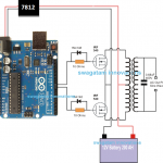
Power Supply
We give +12V to the Vcc pin of both IC IR2111 because that is needed for the internal logic and gate drive stage.
We also see that there is a separate high voltage DC bus shown with red line at the top which can be up to +600V maximum.
That high DC generally comes after rectifying mains AC or from a big DC capacitor bank. The load is connected between the two mid points of the H bridge so that it receives the alternating drive.
IR2111 Driver ICs
Now let us talk about how the IR2111 works. The Vcc pin is +12V, the COM pin is ground, the IN pin is where we feed the PWM signal, the LO pin gives out the low side gate drive, the HO pin gives out the high side gate drive and the VB and VS pins make the bootstrap floating supply for the high side MOSFET.
The A159 diode and 10uF capacitor form the bootstrap. So because of that the high side MOSFET can switch properly even though it is sitting on the floating node.
When we put PWM to IN then the IC automatically makes the HO and LO outputs in correct way and the MOSFET pair gets driven.
Since we are using two ICs, one for each side of the H bridge, so we get both legs of the H bridge controlled. That is how we get AC waveform across the load.
MOSFET H Bridge
The four MOSFETs are arranged in typical H bridge form. Two MOSFETs are connected on the left side and controlled by the left IC and two MOSFETs are on the right side and controlled by the right IC.
The load is fixed right at the center points between these legs. Gate resistors of 10 ohm and pull down resistors of 10k are used at the gates. These resistors make sure that switching is clean and that the MOSFET gates do not float.
Current Sense Resistor Rx
At the very bottom we see the resistor Rx which is the current sensing element. This resistor is in series with the load return path.
So whatever current flows to the load must also pass through Rx. This resistor develops a voltage drop proportional to current because of Ohms law.
If the current is normal then the drop is small and cannot bias the BC547 transistors. But when the current rises too much then the voltage across Rx rises and then it is able to turn on the BC547 base.
Overload Shut Down With BC547
We see two BC547, one on each side of the circuit connected with the IN pins. Their bases are fed through 10k resistors from the Rx sensing resistor.
When the current is in safe region then both BC547 remain off and so the PWM signals enter the IN pins of both ICs without problem.
But when the current rises above safe level then the voltage across Rx becomes high and then it makes the BC547 conduct.
As soon as the BC547 conduct they short the IN pins to ground.
When IN pin is pulled to ground then the IC stops giving output and so the MOSFETs turn off instantly.
This stops the inverter and protects the MOSFETs and the load from further damage.
Sequence Of Working
So what happens step by step is that the PWM generator gives PWM#1 and PWM#2 to the two ICs, then the ICs drive the MOSFETs in proper half bridge fashion, then the MOSFETs switch and create AC at the load, then the load current flows through Rx, then if the current is low the inverter keeps working normally, but if the current rises too high then voltage across Rx becomes high, then BC547 conduct and pull down the IN pins, then the ICs stop and the inverter is shut down until overload is removed.
Formula For Rx
Now about the formula of Rx. The BC547 needs about 0.6 V to start conduction.
So the threshold can be calculated by simple formula Rx = 0.6 divided by Imax.
For example if we want cut off at 10 A then:
Rx = 0.6 / 10 = 0.06 ohm.
The power rating of Rx must also be considered because it will heat. That can be calculated by:
P = (Imax)2 * Rx
= 102 * 0.06
= 6 watts
Another simpler, way is:
P = Voltage drop across Rx * Imax
= 0.6 * 10
= 6 watts
So in this case we need Rx to be a 0.06 ohm 6 W resistor for safe operation.
Advantages
So this circuit becomes very useful because it can work with high DC bus up to 600 V due to IR2111 drivers, it can run inductive loads. Even though the IC does not have a shut down SD pin, yet we can configure a overload and short circuit protection shut down just by using a couple of BC547, and the protection is reliable because it directly disables the IN pins of the driver ICs.
How to Get the PWM#1 and PWM#2 for the H-Bridge.
You can easily get the two alternating PWMs using the following sine table, but you will need an Arduino to program the code and feed the output to the H-Bridge PWM#1 input and PWM#2 input.


Comments
In the circuit where the BC547 transistor is placed and acts as an electronic fuse, when this transistor activates, it causes a short circuit from the PWM circuit to ground. This leads to the burning of components and ICs in the PWM circuit.
The transistor itself also burns out with this connection.
How can we limit the current passing through this fuse to prevent a sudden short circuit and avoid further issues?
Thank you very much for the time you take to answer.
I think you forgot to put the 10k resistor in series with each PWM inputs, as shown in the diagram.
Please make sure to put those series resistors, and then nothing will burn…
Hello Dr.Swagatam
No, there is also a 10k resistor present.
Can we add another circuit or components so that when the fuse activates, the PWM circuit is shut down?
For example, with the help of an op-amp or a relay.
The op-amp itself could manage the left and right PWM and also cut off the PWM circuit when the electronic fuse is activated.
Hi Mazloumi,
If you have added 10k in series with the PWM inputs then there’s no way the PWM circuit can burn while the BC547 shut down is active.
Which PWM circuit are you using, and how did to isolate the PWM1 and PWM2 so that they function alternately and never together, and most importantly when one PWN is active the other PWM source must be 0V….did you make the PWM function in this way??
Dear Mr. Swagatam
Can the PWM be generated with a 555, and can we use an amplifier, for example, a CD4013, to create PWM1 and PWM2 for the left and right inputs of the driver?
Hi Mazloumi, A 4017 IC would work better and allow you to generate even modified output sine wave.
Using the circuit that you sent and adding an electronic fuse.
The PWM is also generated by a 555 astable.
Then you can connect the collector of the BC547 feedback BJT with pin#5 of the IC555, to shut down the 555 output during over current…
1. Is this inverter sine wave?
2. What is it’s power rating?
3. What’s the value of the RX?
4. How do I increase the output power, if I need to?
1.Yes it will be a pure sine wave inverter, if the code given in the sine table is used, and LC filter is used at the output.
https://www.homemade-circuits.com/inverter-lc-filter-calculator/
2. Power will depend on the MOSFET rating.
3. RX = 0.6/Max output current.
4. Upgrade and adjust the rating of the MOSFETs according to the load, also please add snubbers across each MOSFET.
https://www.homemade-circuits.com/rc-snubber-calculator-for-mosfets-relay-contacts-and-triacs/