In this article I have explained regarding how to design and make your own customized high current wireless battery charger circuit using wireless power transfer concept.
Introduction
In many of my earlier articles I have comprehensively discussed wireless power transfer, in this article we will go a step ahead and try to learn how to design a high current version of the same which can be applied for any high power wireless transfer operation such as for charging an electric car battery etc.The idea of optimizing a wireless power transfer circuit is quite similar to optimizing an induction heater circuit, wherein both the concepts can be seen utilizing the optimization of their LC tank stage for achieving the desired power output at the highest possible efficiency.
The design can be implemented by utilizing the following basic circuit stages in it:
The Transmitter Circuit will include:
1) An adjustable frequency oscillator.
2) A half bridge or a full bridge circuit (preferably)
3) BJT/Mosfet driver stage.
4) an LC circuit stage
The Receiver circuit stage will include:
1) Only the LC circuit stage.
An example circuit for the proposed high current wireless battery charger can be witnessed in the following diagram, for simplicity sake I have eliminated the use of a full bridge or half bridge circuit, rather have incorporated an ordinary IC 555 circuit.
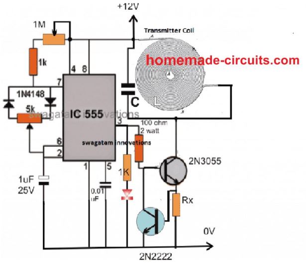
The above design represents the transmitter circuit of the high power wireless battery charger circuit using a IC 555 PWM circuit.
Here the output could be a little inefficient since the conduction process is single sided and not a push pull type.
Still, if this circuit is correctly optimized a decent high current power transfer can be expected from it.
Please remember that the wire inside coil must not be a thick single core wire, rather a bunch of many thin wires. This will allow better absorption of current and therefore higher rate of transfer.
How it Works
The IC 555 is basically configured in its standard PWM mode which can be adjusted using the shown 5K pot, there's another adjustable resistor in the form of 1M pot which can used for optimizing the frequency and the resonance degree of the circuit.
The PWM pot could be used for adjusting the current level while the 1M for peaking the resonance level of the LC tank circuit.
The LC tank circuit can be seen attached with the transistor 2N3055 which powers this LC stage with a frequency corresponding to its base frequency from pin#3 of the IC.
How to Select the LC Components.
Selecting the LC parts optimally can be achieved by following the instructions as furnished in this article which explains how to optimize resonance frequency of an LC tank network.
Basically if you know the frequency value, and either L or C, then the unknown parameter can be easily calculated using the suggested formula or this LC resonance calculator software.
The Receiver Circuit
The coil for the receiver circuit for this high current wireless battery charger is exactly similar to the transmitter coil. Meaning, you can simply use a single continuously running coil from start to end, and add a resonating capacitor across these terminals.
Make sure the LC values are exactly similar to the Tx LC values. The set up can be seen in the following image:
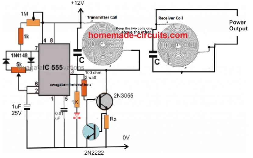
The 2N2222 transistor is introduced to make sure that while adjusting the resonance, the 2N3055 is never subjected to an over current situation. In case this tends to happen the over current develops an equivalent amount of triggering across Rx sufficient to activate the 2N2222, which in turn shorts the 2N3055 base to ground inhibiting it from conducting any further and thus preventing the device from a possible damage.
Rx may be calculated using the following formula:
Rx = 0.6/Max current Limit of the transistor (or the wireless power transfer)
Adding a voltage regulator for charging the battery:
In the above diagram, the output from the receiver should be attached with a voltage regulator circuit such as using an LM338 circuit or an opamp controller circuit for making sure that the output can be safely fed to the intended battery for charging it.
If you have any further queries, please feel free to express them through your comments.
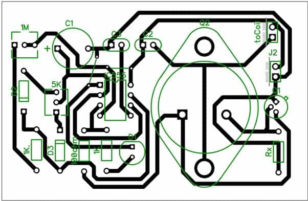
PCB Layout

Comments
please support as some component without data in DC Wireless charger diagram.
This guy seems to have a whole bunch of badass projects. And I will always spend my time trying to recreate all of them just for fun. The only hard part is my funding, wish I could have been a teacher, thanks for sharing your schematics and taking the time and effort because I know how much every goes in the posting
Sir, Good morning to you. Unable to find a solution from any where I have turned to your website as a last resort. I need to travel cross country in car, using Google maps. The travel time sometimes last for 4-5 hours. I am using ASUS ZenFone for the purpose. I face great difficulty in charging the mobile while continuing to use Google maps for navigation. In spite of keeping the mobile connected to the adaptor charger, ultimately the mobile's battery drain out completely after about 3-4 hours. I have tried no of adopters, but none could solve my problem. The mobile get / remains fully charged when connected to 10000mAh power bank. I have opened two of the adopters and found one of them using IC MC54063AN,photo attached as (A)and other one using IC XC1530E, photo attached as (B). Please help me in modification of the circuitry to increase the charging current of these adopters. I am a 3years diploma in ECS. I will be able to follow your advice on the matter. Thanks ®ards.
Debasis, OK got it, so it seems to be a DC to DC adapter…
you can try modifying your adapter output by changing the wire thickness of the buck inductor associated with the IC.
You might have noticed that the circuit has an inductor, you will need to carefully remove the inductor, unwind the turns, and then take two exactly similar wires together and re-wind it with the same number of turns. this will hopefully increase the current output of the system and speed up the charging process.
Sir, so kind of you to try to answer and notify me so promptly. Input to the adaptor is from cigarette lighter socket of the car I use for traveling. The car battery is 12 volts. Though the adopters stated output current 1.7 amps, but practically it sure to be much less. I came to this conclusion because for testing when when I simulate same situation as I practically undergo while traveling by charging the mobile from the OEM supplied AC mains adopter of stated output voltage and current of 5.2 v and 1.2 amps respectively, the phone works fine even when I continuously fiddle the Google maps. The adopter continue to increase the amount of charge of the phone. Untimely the phone gets fully charged over a period of 2.5 to 3 hours. I hope you got the idea input and output of these DC to DC adopters. Regards
Good morning Dabasis, yes it is most probably due to lower current from the adapter unit that's causing a slower charging of the mobile battery and unable to match the consumption rate.
By the way while travelling how do you access the mains supply for the adapter? or are these adapters DC to DC types?
You can also confirm the amps from the two units by measuring them through a DMM or an ammeter.
Please provide the details of the adapter whether it's an AC to DC or DC to DC so that I am able to suggest improvements….
please what is the current output and what's it range… thanks
6 inches
Well done and innovations