We all have heard a lot about buck and boost circuits and know that basically these circuits are used in SMPS designs for stepping up or stepping down a given voltage at the input. The interesting thing about this technology is that it allows the above functions with negligible heat generation which results in a extremely efficient conversions.
What is Buck-Boost, How it Works
I have explained the concept in the first section without involving much technicalities so that it becomes easier to understand what's exactly buck boost concept even to a newbie.
Among the three fundamental topologies named buck, boost, and buck-boost, the third one is more popular since it allows both the functions (buck boost) to be used through a single configuration just by altering the input pulses.
In the buck-boost topology we primarily have an electronic switching component which can be in the form of a transistor or a mosfet. This component is switched via a pulsating signal from an integrated oscillator circuit.
Apart from the above switching component, the circuit has an inductor, a diode and a capacitor as the main ingredients.
All these parts are arranged in the form that may be witnessed in the following diagram:
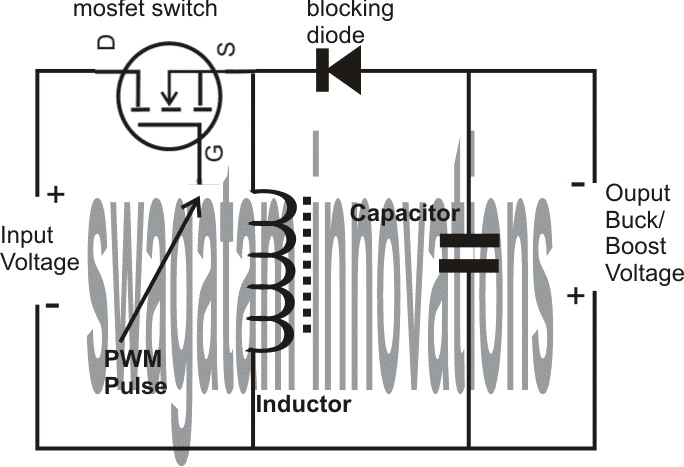
Referring to the above buck boost diagram, the mosfet is the part which receives the pulses which forces it to operate under two conditions: ON state and OFF state.
During ON state the input current gets a clear path through the mosfet and instantly tries to make it's way across the inductor since the diode is positioned in the reversed biased state.
The inductor on account of its inherent property tries to restrict the sudden infliction of current and in an compensating response stores some quantity of current in it.
Now as soon as the mosfet is switched OFF it goes under the OFF state blocking any passage of the input current.
Again the inductor is unable to cope with this sudden change of current from a given magnitude to zero, and in a response to compensate this, it kick backs its stored current via the diode across the output of the circuit.
In the process the current also gets stored in the capacitor.
During the next ON state of the mosfet, the cycle is repeated as above however with no current available from the inductor, the capacitor discharges the stored energy into the output which helps in keeping the output stable to the optimized degree.
You may be wondering what factor decides the BUCK or the BOOST results at the output? It's quite simple, it depends on how long the mosfet is allowed to stay in the ON state or in the OFF state.
With an increase in the mosfets ON time, the circuit starts getting transformed into a Boost converter while with the mosfets OFF time exceeding its ON time results in the circuit behaving like a Buck converter.
Thus the input to the mosfet can be made through an optimized PWM circuit for getting the required transitions across the same circuit.
Exploring Buck/Boost Topology in SMPS Circuits More Technically:
As discussed in the above section the three fundamental topologies which are popularly used with switch mode power supplies are the buck, boost, and the buck boosts.
These are basically non-isolated in which the input power stage shares a common base with the output power section. Of course we could also find isolated versions although pretty rare.
The above expressed three topologies can be distinguished uniquely depending upon their exclusive properties.The properties may be identified as the steady state voltage conversion ratios, the nature of the input and output currents and the character of the output voltage ripple as well.
Additionally the frequency response of the duty cycle to the output voltage execution can be considered as one of the important properties.
Among the above referred three topologies, buck-boost topology is the most preferred one because it allows the output to work voltages less than the input voltage (buck mode) and also to produce voltages above the input voltage (boost mode).
However the output voltage can be acquired always with the opposite polarity from the input, which doesn't create any issues whatsoever.
The applied input current to a buck boost converter is the form of a pulsating current due to the switching of the associated power switch (Q1).
Here the current switches from zero to l during every pulse cycle.The same is true for the output also and we get a pulsating current because of the associated diode which conducts only in one direction, causing an ON and OFF pulsating situation during the switching cycle.
The capacitor is responsible for providing the compensating current when the diode is in the switched OFF or reverse biased state during the switching cycles.
This article explains steady state functionality of the buck-boost converter in continuous-mode and discontinuous-mode operation with exemplary waveforms presented.
The duty-cycle-to-output voltage exchange functionality is presented after an introduction of the PWM switch design.
Figure 1 a simplistic schematic of the buck-boost power stage with a drive circuit block added. The power switch, Q1, is an n-channel MOSFET. The output diode is CR1.
The inductor, L, and capacitor, C, constitute the efficient output filtering. The capacitor ESR, RC, (equivalent series resistance) and the inductor DC resistance, RL, are all analyzed in this article . The resistor, R, corresponds to the load as indicated by the power stage output.
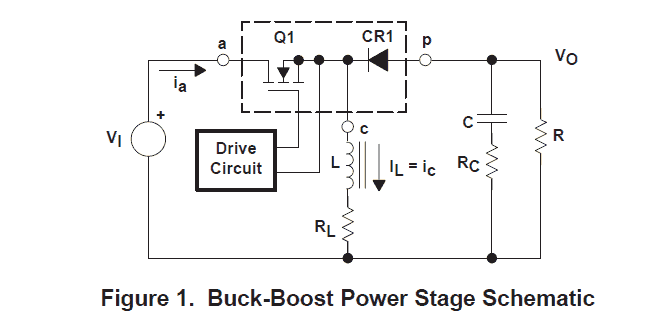
In the course of regular functionality of the buck-boost power stage, Q1 is constantly turned on and off with the on- and off-times governed by the control circuit.
This switching behavior results in a chain of pulses at the junction of Q1, CR1, and L.
Even though the inductor, L, is linked to the output capacitor, C, if only CR1 conducts, a successful L/C output filter is established. It cleans the succession of pulses to result in a DC output voltage.
Buck-Boost Stage Steady-State Analysis
A power stage may function in continuous or discontinuous inductor current setting. Continuous inductor current mode is identified by current continuously in the inductor over the switching sequence in steady-state process.
Discontinuous inductor current mode is identified by the inductor current staying zero for a section of the switching cycle. It begins at zero, extends to a maximum value, and comes back to zero in the course of every switching pattern.
The two distinct methods are mentioned in much larger detail afterwards and model suggestions for the inductor value to sustain a selected mode of functionality as the ability of rated load are presented. It is rather favorable for a converter to be in a single format only over its predicted functioning circumstances since the power stage frequency response alters substantially between the two distinct techniques of operation.
With this assessment, an n-channel power MOSFET is employed and a positive voltage, VGS(ON), is supplied from the Gate to the Source terminals of Q1 by the control circuit to switch on the FET. The benefit of employing an n-channel FET is its lower RDS(on) however the contro circuit tricky because a suspended drive becomes necessary. For the identical package dimensions, a p-channel FET possesses a higher RDS(on) nonetheless typically may not necessitate a floating drive circuit.
The transistor Q1 and diode CR1 are illustrated inside a dashed-line outline with terminals tagged a, p, and c. It is discussed thoroughly in the Buck-Boost Power Stage Modeling portion.
Buck-Boost Steady-State Continuous Conduction Mode Analysis
The following is a description of buck boost working in the steady-state operation in continuous conduction method. The primary objective of this segment would be to present a derivation of the voltage transformation relationship for the continuous conduction mode buck-boost power stage.
This will be significant since it indicates the way the output voltage is determined by duty cycle and input voltage or on the contrary, how the duty cycle could be determined depending on input voltage and output voltage.
Steady-state means that the input voltage, output voltage, output load current, and duty-cycle are constant as opposed to varying. Capital letters are usually provided to variable labels to suggest a steady-state magnitude. In continuous conduction mode, the buck-boost converter takes a couple of states per switching cycle.
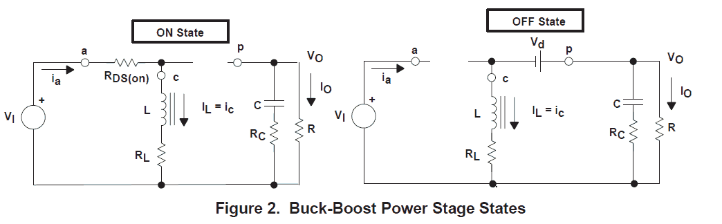
The ON State is each time Q1 is ON and CR1 is OFF. The OFF State is every time Q1 is OFF and CR1 is ON. An easy linear circuit could symbolize each of the two states in which the switches in the circuit are substituted by their matching circuit in the course of each state. The circuit diagram for each of the two conditions is presented in Figure 2.
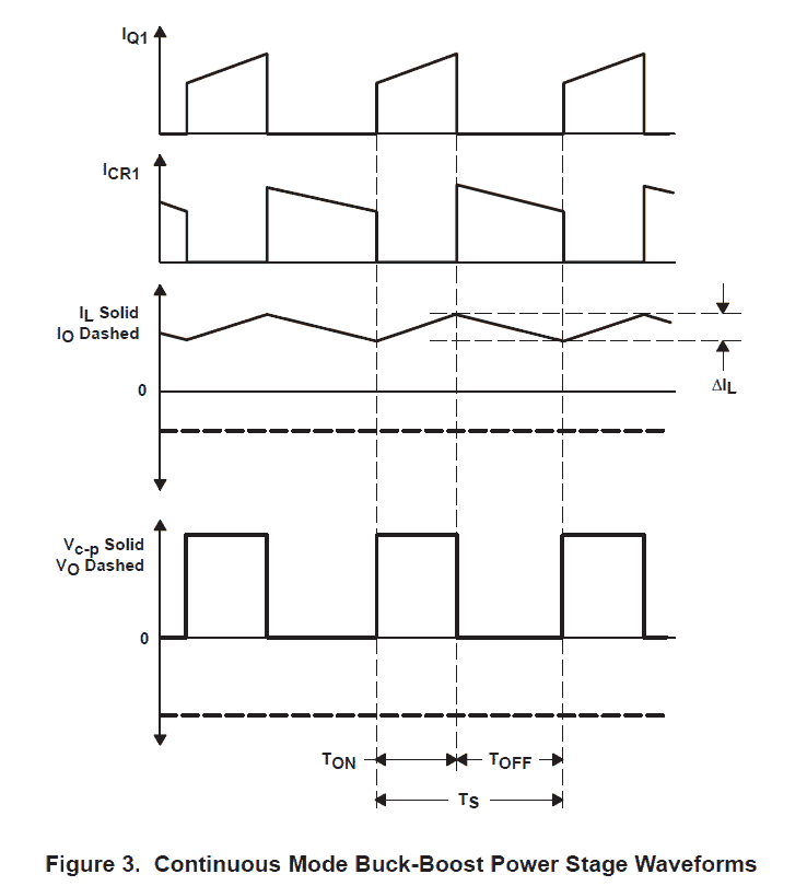
The period of the ON condition is D × TS = TON in which D is the duty cycle, fixed by the drive circuit, depicted in form of a ratio of the switch ON period to the period of a single full switching sequence, Ts.
The length of the OFF state is known as TOFF. Because one can find just a couple of conditions per switching cycle for continuous conduction mode, TOFF is equal to (1−D) × TS. The magnitude (1−D) is occasionally called D’. These periods are presented together with the waveforms in Figure 3.
Looking at Figure 2, in the course of the ON state, Q1 offers a reduced resistance, RDS(on), from its drain to source and manifests a smaller voltage drop of VDS=IL × RDS(on).
Additionally there is a little voltage drop across the dc resistance of the inductor equal to IL × RL.
Thereby, the input voltage, VI, minus deficits, (VDS + IL × RL), is put on across the inductor, L. CR1 is OFF within this period as it would be reverse biased.
The inductor current, IL, passes from the input supply, VI, by way of Q1 and to ground. In the course of the ON state, the voltage put on across the inductor is constant and the same as VI − VDS − IL × RL.
Following the polarity norm for the current IL presented in Figure 2, the inductor current boosts due to the executed voltage. Furthermore, because the applied voltage is fundamentally consistent, the inductor current rises linearly. This boost in inductor current in the course of TON is drawn out in Figure 3.
The level by which the inductor current boosts is generally determined by utilizing a form of the well-known formula:
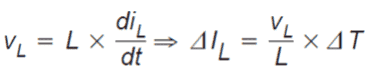
The inductor current rise in the course of the ON status is presented as:
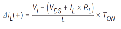
This magnitude, ΔIL(+), is termed the inductor ripple current. Furthermore observe that through this interval, every bit of the output load current comes in by the output capacitor, C.
With reference to Figure 2, while Q1 is OFF, it offers an increased impedance from its drain to source.
Consequently, because the current running in the inductor L is unable to adjust instantly, the current switches from Q1 to CR1. As a result of the reducing inductor current, the voltage across the inductor reverses polarity until rectifier CR1 turns into forward biased and flips ON.
The voltage connected across L turns into (VO − Vd − IL × RL) in which the magnitude, Vd, is the forward voltage drop of CR1. The inductor current, IL, at this point passes from the output capacitor and load resistor arrangement via CR1 and to the negative line.
Observe that the alignment of CR1 and the path of current circulation in the inductor signifies that the current running in the output capacitor and load resistor grouping leads to VO to be a minus voltage. In the course of the OFF state, the voltage connected across the inductor is stable and the same as (VO − Vd − IL × RL).
Preserving our likewise polarity convention, this connected voltage is minus (or reverse in polarity from the connected voltage in the course of the ON time), due to the fact that the output voltage VO is negative.
Therefore, the inductor current lowers throughout the OFF time. Furthermore, because the connected voltage is basically steady, the inductor current reduces linearly. This reduction in inductor current in the course of TOFF is outlined in Figure 3.
The inductor current reduction through the OFF situation is provided by:
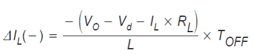
This magnitude, ΔIL(−), can be termed the inductor ripple current. In stable state situations, the current rise, ΔIL(+), in the course of the ON time and the current reduction through the OFF time, ΔIL(−), has to be identical.
Or else, the inductor current could offer an overall boost or reduction from cycle to cycle that would not be a stable condition circumstance.
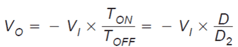
Thus, both of these equations may be equated and worked out for VO to acquire the continuous conduction form buck-boost voltage change-over affiliation:
Determining for VO:
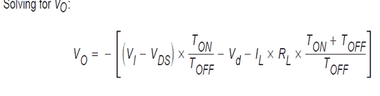
As well as, substituting TS for TON + TOFF, and employing D = TON/TS and (1−D) = TOFF/TS, the steady-state equation for VO is:
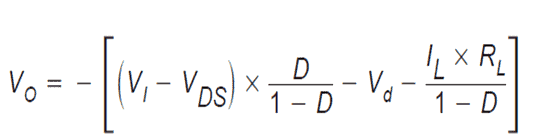
Observe that in simplifying the above, TON + TOFF is supposed to be similar to TS. This can be genuine only for continuous conduction mode as we are going to discover in the discontinuous conduction mode evaluation. An essential scrutiny ought to be made at this point:
Fixing the two values of ΔIL on par with each other is exactly equal to leveling out the volt-seconds on the inductor. The volt-seconds employed on the inductor is the product of the voltage employed and the period that the voltage is applied for.
This can be the most effective way to estimate unidentified magnitudes for example VO or D with regards to common circuit parameters, and this approach is going to be used frequently within this article. Volt-second stabilize on the inductor is a natural requirement and ought to be perceived at least additionally as Ohms Law.
In the above equations for ΔIL(+) and ΔIL(−), the output voltage was implicitly supposed to be consistent without any AC ripple voltage throughout the ON time and the OFF period.
This is an accepted simplification and entails a couple of individual outcomes. First, the output capacitor is believed to be sizable adequately that its voltage conversion is minimal.
Second, the voltage the capacitor ESR is in addition deemed to be minimal. Such assumptions are legitimate since the AC ripple voltage will definitely be significantly lower than the DC portion of the output voltage.
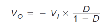
The above voltage alteration for VO demonstrates the truth that VO could be tweaked by fine-tuning the duty cycle, D.
This connection draws near zero as D arrives near zero and rises without destined as D draws near 1. A typical simplification consider VDS, Vd, and RL are tiny enough to neglect. Establishing VDS, Vd, and RL to zero, the above formula simplifies noticeably to:
A less complicated, qualitative method to picture the circuit operation would be to contemplate the inductor as a power storage part. Each time Q1 is on, energy is poured over the inductor.
While Q1 is off, the inductor supplies back part of its energy to the output capacitor and load. The output voltage is regulated by establishing the on-time of Q1. For instance, by raising the on-time of Q1, the quantity of power sent to the inductor is amplified.
Additional energy is subsequently sent to the output in the course of the off-time of Q1 causing an increase in the output voltage. In contrast to the buck power stage, the typical magnitude of the inductor current is not the same as the output current.
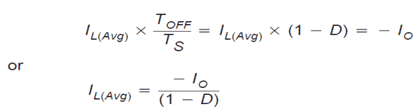
To associate the inductor current to the output current, looking at Figures 2 and 3, observe that the inductor current to the output solely while in the off state of the power stage.
This current averaged over a whole switching sequence is the same as the output current since the approximate current in the output capacitor ought to be equivalent to zero.
The connection between the average inductor current and the output current for the continuous mode buck-boost power stage is provided by:
Another significant viewpoint is the fact the typical inductor current is proportional to the output current, and because the inductor ripple current, ΔIL, is unrelated of output load current, the minimal and the highest values of the inductor current follow the average inductor current precisely.
As an example, if the average inductor current declines by 2A owing to a load current reduction, in that case the lowest and highest values of the inductor current reduce by 2A (considering continuous conduction mode is preserved).
The forgoing evaluation was for the buck-boost power stage functionality in continuous inductor current mode. The following segment is a explanation of steady-state functionality in discontinuous conduction mode. The primary outcome is a derivation of the voltage conversion relationship for the discontinuous conduction mode buck-boost power stage.
Buck-Boost Steady-State Discontinuous Conduction Mode Evaluation
We at this point examine what occurs where the load current is reduced and the conduction mode shifts from continuous to discontinuous.
Remember for continuous conduction mode, the average inductor current trails the output current, i.e. in case the output current reduces, in that case so will the average inductor current.
Besides, the lowest and highest peaks of the inductor current pursue the average inductor current accurately. In case the output load current is decreased below the fundamental current level, the inductor current would be zero for a part of the switching sequence.
This would be apparent from the waveforms presented in Figure 3, because the peak to peak level of the ripple current is unable to alter with output load current.
In a buck-boost power stage, if the inductor current tries to below zero, it simply halts at zero (because of the unidirectional current movement in CR1) and continues there until the outset of the subsequent switching action. This working mode is known as discontinuous conduction mode.
A power stage working of buck boost circuit in discontinuous conduction format possesses three distinctive states through every switching cycle in contrast to 2 states for continuous conduction format.
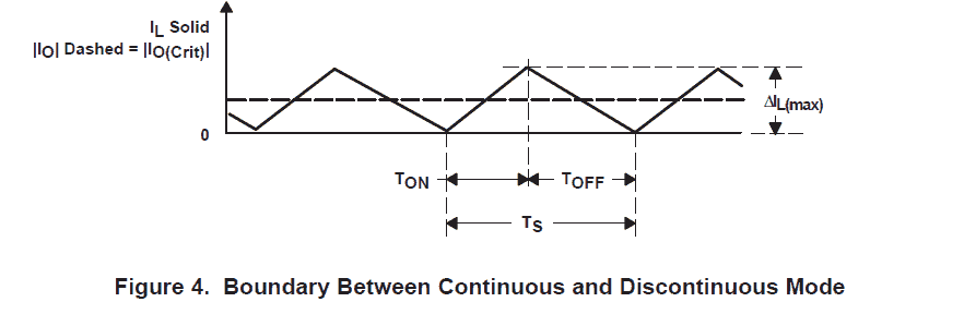
The inductor current state in which the power stage is at the periphery between continuous and discontinuous setting is presented in Figure 4.
In this the inductor current simply collapses to zero while the following switching cycle commences just after the current attains zero. Observe that the values of IO and IO(Crit) are laid out in Figure 4 since IO and IL include opposing polarities.
Farther lowering of output load current sets the power stage into discontinuous conduction pattern. This condition is drawn in Figure 5.
The discontinuous mode power stage frequency response is pretty dissimilar from the continuous mode frequency response which is presented in the Buck-Boost Power Stage Modeling segment. Additionally, the input to output connection is fairly diverse as presented down this page derivation:
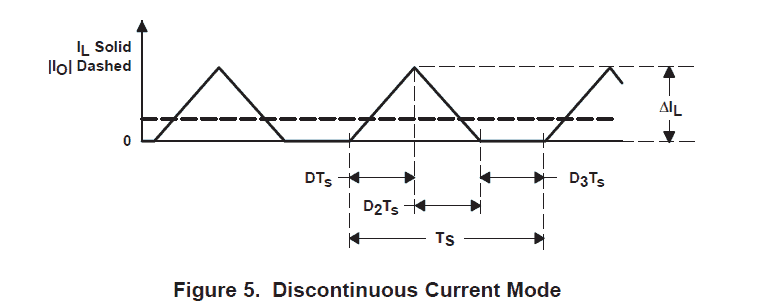
To start the derivation of the discontinuous conduction mode buck-boost power stage voltage change-over ratio, recollect that you have three distinctive states that the converter considers through discontinuous conduction mode functionality.
The ON State is when Q1 is ON and CR1 is OFF. The OFF State is when Q1 is OFF and CR1 is ON. The IDLE condition is when each Q1 and CR1 are OFF. The initial two conditions are very much like the continuous mode situation and the circuits of Figure 2 are relevant apart from that TOFF ≠ (1−D) × TS. The rest of the switching sequence is the IDLE state.
Additionally, the DC resistance of the output inductor, the output diode forward voltage drop, as well as the power MOSFET ON-state voltage drop are usually supposed to be minute enough to overlook.
The time period of the ON state is TON = D × TS where D is the duty cycle, fixed by the control circuit, indicated as a ratio of the turn on time to the time of one full switching sequence, Ts. The length of the OFF state is TOFF = D2 × TS. The IDLE period is the rest of the switching pattern which is presented as TS − TON − TOFF = D3 × TS. These periods are put up with the waveforms in Figure 6.
Without checking the comprehensive description, the equations for the inductor current rise and drop are enumerated below. The inductor current rise in the course of the ON state is issued by:
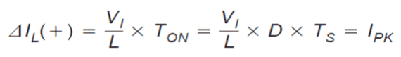
The ripple current quantity, ΔIL(+), is likewise the peak inductor current, Ipk since in discontinuous mode, the current begins at 0 every cycle.The inductor current reduction in the course of the OFF state is presented by:
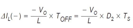
Just like the continuous conduction mode situation, the current rise, ΔIL(+), in the course of the ON time and the current reduction while in the OFF time, ΔIL(−), are identical. Thus, both of these equations could be equated and addressed for VO to acquire the initial of two equations to be utilized to solve for the voltage conversion ratio:
Next we determine the output current (the output voltage VO divided by the output load R). It is the average over one switching sequence of the inductor current at that time when CR1 becomes conductive (D2 × TS).
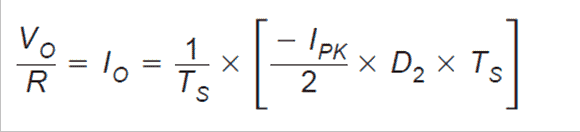
Here, replace the connection for IPK (ΔIL(+)) into the above equation to acquire:
Therefore we have two equations, the one for the output current (VO divided by R) just derived and the one for the output voltage, both of them with regards to VI, D, and D2. We at this point unravel each formula for D2 as well as fix the two equations on par with one another.
Utilizing the resultant equation, an illustration for the output voltage, VO, could be procured. The discontinuous conduction mode buck-boost voltage transformation affiliation is written by:
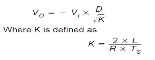
The above connection displays one of the main dissimilarities between the two conduction modes. For discontinuous conduction mode, the voltage change relationship is a function of the input voltage, duty cycle, power stage inductance, the switching frequency, and the output load resistance.
For continuous conduction mode, the voltage change-over connection is just influenced by the input voltage and duty cycle. In traditional applications, the buck-boost power stage is run in a choice between continuous conduction mode or discontinuous conduction mode. For a specific usage, one conduction mode is chosen while the power stage was made to sustain the identical mode.


Comments
Dear Swagatam Sir,
Thank you for making this information public… I have some old solar panels that I use as a roof for my terrace and carport. I do not want to buy expensive batteries or an inverter.
My only goal is to heat the water tank’s heating element using these solar panels. Since I do not need batteries or inverter, I thought I could directly power the heater.
I understood from your article that this cannot be directly connected.
I can build a PWM controller using a transformer (ferrite) on the primary side with ADC voltage and current sensing to perform MPPT.
My question is about the secondary side:
Is it OK if I rectify the secondary coil, add a capacitor, then connect all the secondaries in series and connect the heater element directly?
The heater is a 10A load, so I would put 7 solar panels in series. But each panel will produce different power because of orientation, chimney shadow, clouds, etc.
So the question is:
Since the secondaries are in series, the current will be the same through all of them, but their voltages will differ. Is that OK, or do I need to add a separate current-regulated buck-boost converter after each rectified secondary?”
Thank you Dear András, I am glad you liked the above article explanation…
However, yes, if the panels are mismatched or shaded differently then you cannot put them in series directly without giving each panel its own converter. Because you must give every single panel its own small Buck-Boost MPPT DC-DC stage so that each panel can work in its own best point.
Why this happens? When you put panels in series then the weakest panel in that line will limit the current for the whole string. When there is mismatch then it creates power loss and unwanted heating and sometimes even reverse bias problems. So a single MPPT cannot optimize every panel when each panel is working under different sunlight conditions.
So now the correct method becomes very simple. We let each panel get one MPPT Buck-Boost stage and then we let you connect the outputs of all those MPPTs in series or in parallel as you need. This works exactly like micro-optimizers work in commercial systems.
Please let me know if you have any further doubts regarding the topic….
Köszönöm a segítséget!
My pleasure….
I’m trying to make a 13.8 v dc to 48 v dc 20 amps boost converter. all the circuits I come across fall short on the output current.
This is for use in a car the input is 13.8 v dc and I need 48v dc @ 20 amps output.
To accomplish this your car battery must be able to produce 80 amps every one hour. And if the required backup time is minimum 5 hours then the battery Ah rating should 80 x 5 = 400 Ah.
So if your car battery is rated at 12v 400 Ah then you can achieve this intended results.
No the cars electrical system needs to provide 960 watts + 20% for conversion loss for a total of 1152 watts continuously…. That’s Not the point I’m looking for a practical circuit .
You can try the following circuit. Upgrade the MOSFET, coil and the zener diode to achieve the intended results.
https://www.homemade-circuits.com/wp-content/uploads/2023/07/laptop-charger-12-V-to-19V-converter-circuit-768×397.jpg
When you increase the voltage, the current will come down proportionately.
Basically the Output Power will be = 90% or 80% of Input Power.
Hi Swagatham
I can not see which MOSFET you are using?
Thank you again.
Hi Warren,
The MOSFET specification will depend on the load specification. Normally you can use a IRF540 or for higher loads you can use IRF3205
swagatham sir i want 12v dc to 50v dc 30amp .buck converter ckt diagram. iam using 12v 63ah battery.
12v dc to 50v dc 30@ 30 amps is a boost converter.
Sree, you can try the first circuit from this post:
https://www.homemade-circuits.com/12v-car-laptop-charger-circuit-using/
He wants 50v dc @ 30 amps this circuit will not work
It will certainly work with some basic modifications…
Hi sir can I use the first circuit in post for boosting 6v upto 8v, and can I use AMV for pwm pulses.
Hi Abhishek, you can try it. You can also try any joule thief circuit
Hi swagatam,plz provide me some help regarding bk-bst converter ckt witk solar panel for pump load with these conditions.1)solar panel (two 12v/1.08A(total 40w) panel in series). 2)a dc pump load(24v/0.4A). The problem is that the ckt should perfm buck for vg>24v and bst opn for vg<24v with i/p vg varing btn 15-34.Arduino is used for duty cycle.help me to choose L&C value.Also any suggestion regarding circuit.