In this child crying monitor circuit when the baby wakes up in their room, the parents are immediately notified, even if they are in another room of their home. A sensor detects the crying sound accompanying the wake-up. After appropriate processing, it sends a signal through the 220V power lines. The receiver, connected to any electrical outlet, amplifies these signals and emits a series of warning beeps.
By: Rudolf Kenny
Warning: The circuits presented below consist of lethal 220V potentials which can be life threatening if not handled correctly. Users are advised to follow appropriate precautions.
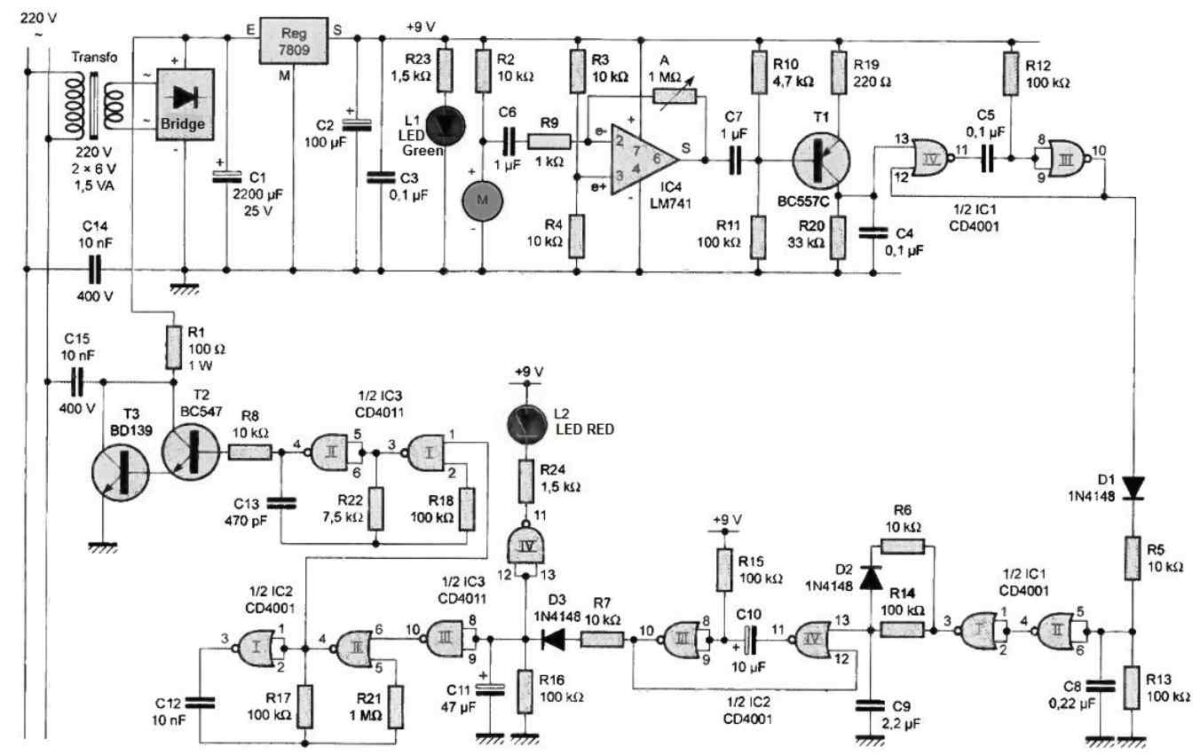
Power Supply
The energy for the detector-transmitter (photo A) comes from the 220V mains supply via a transformer delivering a potential of 12V on its secondary winding.
A bridge rectifier rectifies the two alternating currents, while capacitor C1 provides initial filtering. On the output of regulator 7809, a stabilized DC potential of 9V is obtained. Capacitor C2 performs additional filtering, while C3 decouples the power supply from the circuit. The green LED L1, whose current is limited by R23, indicates the power-on status of the circuit.
Detection of Sound
An electret microphone is used to pick up the sounds emitted in the room under surveillance. It should be noted that such a component includes a built-in preamplifier. The signals available on the positive terminal are transmitted to the inverting input (2) of the op-amp 104 through C6 and R9. The non-inverting input (3) is subject to half the power supply potential through the resistor bridge formed by R3 and R4.
This potential is also available at the output (6) of the op-amp in the absence of sound.
With adjustable resistor A, it is possible to adjust the gain of the amplifier from 0 to 1000 according to the formula: Gain = A/R9.
The signals output from IC4 are transmitted to the base of transistor PNP/T1 through C7.
Discrimination between very short and longer noises
From the beginning of the "high" state on the output of NOR gate 1C1, capacitor C9 begins charging through R14. Its positive plate reaches half the power supply potential after a duration of about 30 ms. It is at this moment that the monostable flip-flop formed by NOR gates III and IV of IC2 is triggered, delivering a "high" state on its output characterized by a duration of about 700 ms.
The integrator device formed by D3, R7, R16, and C11 then presents, at the combined inputs of NAND gate III of IC3, a pseudo-"high" state, while the output of this same NAND gate delivers a "low" state for at least 3 s. The output of NAND gate IV of IC3 also goes to the "low" state, which allows the red signal LED L2 to light up.
On the other hand, if the duration of the "high" state available on the output of NOR gate 1C1 is less than 30 ms, which is characteristic of short noises (such as those made by a falling object or a brief cough), the positive plate potential of C9 does not have enough time to reach half the power supply potential. This results in the signal corresponding to this noise being ignored and eliminated.
Note that, in this case, C9 discharges very quickly through D2 and R6 in order to be ready for a new solicitation.
Generation of the signal to be processed by the power stage
As soon as input 6 of the astable oscillator formed by NOR gates I and II of IC2 is set to "low", it becomes active. It delivers on output 4 of gate II a square wave signal characterized by a period of about 2.2 ms, which corresponds to a frequency of about 450 Hz.
Note that this output presents a permanent "low" state during the inactive phases of the oscillator. For each "high" state delivered by the oscillator described above, a second oscillator consisting of NAND gates I and II of IC3 becomes active. It delivers a square wave signal on its output with a period of about 8 µs, which corresponds to a frequency of almost 120 kHz. This is the carrier frequency of the low-frequency 450 Hz signal.
Injection of signal into the sector
The NPN transistors T2 and T3 form a power Darlington pair.
It should be noted that such a circuit essentially achieves very high current amplification.
The potential in relation to the collectors through R1 comes from the positive plate of C1.
It is about 18 to 20 V. This value contributes to the increase in the power of the injected signal.
The connection to the mains is made by capacitors C14 and C15. These are capacitors characterized by a voltage insulation of 400 V.
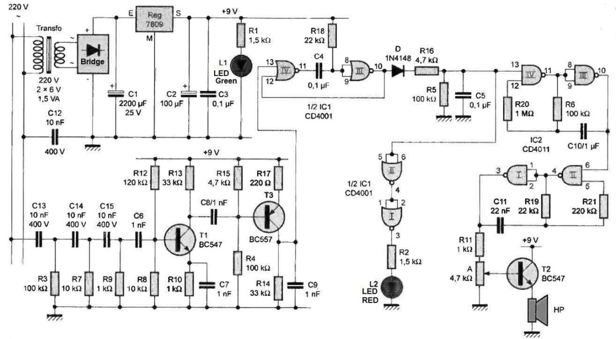
Receiver Power supply
The power supply of the receiver (photo B) is identical in every respect to that of the detector-emitter (Figure 3).
Amplification of signals from the mains
The set of components consisting of C13, R3, C14, R7, C15, and R9 forms a filter designed to receive signals from the 220 V mains.
On the collector of transistor T1, the 120 kHz ripples characteristic of the active phases of the signal emitted by the detector-emitter (Figure 4) are observed. Recall that the latter are presented in the form of a sequence characterized by a periodicity of about 2.2 ms.
Transistor T3, on the other hand, has its base biased to present a zero potential in the rest state.
However, when the detector-emitter is active, a series of ripples are recorded on the collector of T3, whose minima and maxima are close to the supply potential, given the smoothing realized by capacitor C9.
Integration of signals
The signals available on the collector of T3 are taken into account by the NOR III and IV monostable flip-flop of 1C1.
The latter delivers a series of "high" states with a duration of about 1.5 ms. The integrator device consisting of D, R16, R5, and C5 then presents, on the combined inputs of the NOR II gate of IC1, a pseudo "high" state, resulting in a "high" state on the output of the NOR I gate of 1C1 and the illumination of the red LED L2.
Audible Alarm signal
As soon as input No. 13 of the astable oscillator formed by NAND III and IV gates of IC2 is subjected to a "high" state, it becomes active. In particular, it generates a square wave signal with a period of 0.25 s on its output.
During the "high" states of this signal, the NAND I and II oscillator of IC2 goes into action by delivering a square wave signal characterized by a period of about 1 ms, which corresponds to a musical frequency of about 1 kHz. The miniature loudspeaker reproduces this signal in the form of a series of "beeps".
Depending on the angular position of adjustable A, it is possible to obtain a more or less powerful sound output.
Circuit Diagram Child Cry Detector Stage
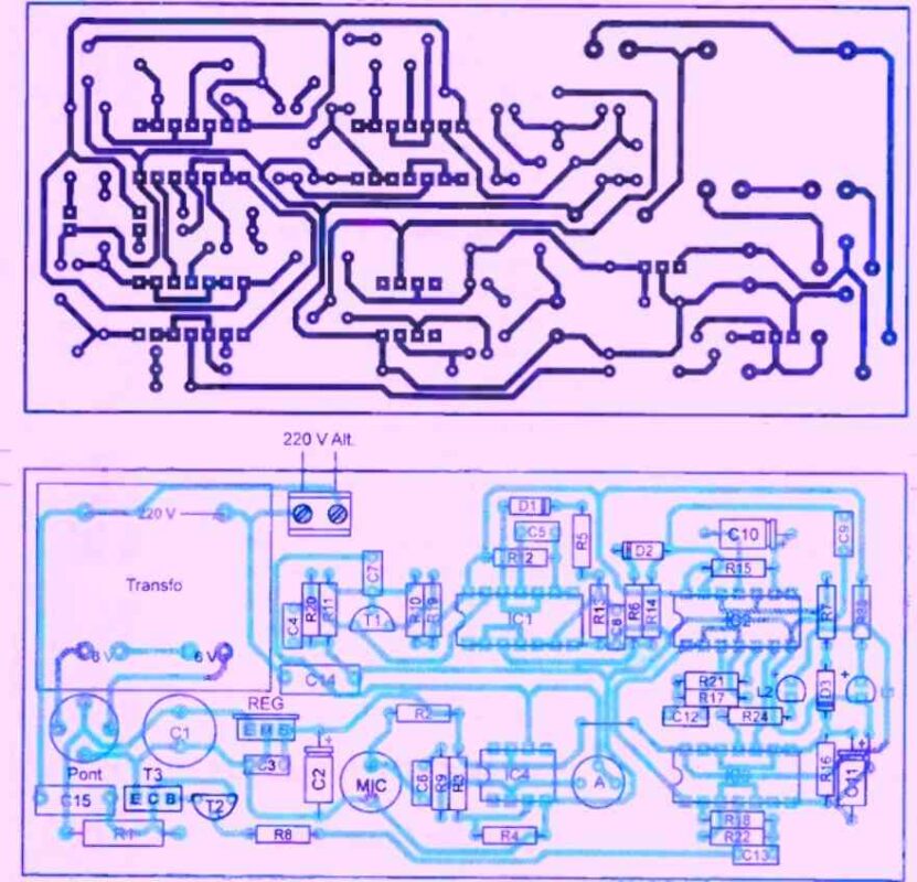
PCB Design
Circuit Diagram Child Cry Alarm Stage
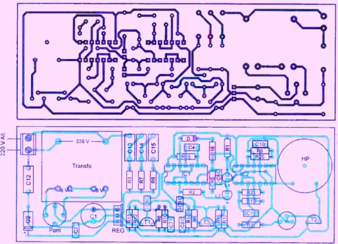
PCB Design


Comments
where are the 2 circuits interconnected
thank you
They are connected through the mains AC power line.