The post presents an in-depth discussion regarding the construction details of a universal high power amplifier which can be modified or adjusted to suit any range within 60 watt, 120 watt, 170 watt or even 300 watt power output (RMS).
The Design
The circuit diagram in Fig. 2 tells about the highest power capability form of the amplifier, this offers 300 W into 4 ohms. Settings to moderate the power output will undoubtedly be talked over afterwards within the post.
The circuit relies upon the a couple of series hooked up MOSFETs, T15 and T16., actually being powered in anti-phase by a differential amplifier. Given that the input resistance of MOSFETs is of the level of 10 ohms, the drive electrical power really needs to be simply modest. The MOSFETs are as a result voltage- operated.
The driver stage is made up predominantly of T1 and T3 together with T12 and T13. Negative d.c. feedback through the output stage is supplied by R22 and negative a.c. feedback by R23----C3.
The a.c. voltage gain is roughly about 30 dB. The below cut-off frequency is determined by the values of C1 and C3. The working purpose of the first differential amplifier, T1, T2 is scheduled by the current streaming through T3.
The collector current of T5 ascertains the reference current for current mirror T3-T4. To make sure that that the referral current is constant, the base voltage of T5 is well controlled by diodes D4-D5.
The output of T1-T2 operates another differential amplifier, T12-T13, whose collector currents establish the gate potential for the output transistors. The measure of that potential would depend on the working position of T12-T13.
Current mirror T9 and T10 together with diodes D2-D5 hold the identical function as T3-T4 and D4-D5 in the first differential amplifier.
The significance of the referral current is characterized by the collector current of Tm, which often is scheduled by P2 in the emitter circuit of T11. This particular combination models the quiescent (bias) current without the presence of (an input signal.
Stabilization of quiescent current
The MOSFETs possess a positive temperature coefficient each time their drain current is nominal, guaranteeing that the quiescent (bias) current is simply maintained consistent by applicable compensation.
This is often made available from R17 over current mirror T9-T10, which includes a negative temperature coefficient. Once this resistor warms up, it begins drawing a relatively more substantial percentage of the reference current via T9.
This brings about a decrease in the collector current of T10 which, sequentially, brings about reduction in the gate-source voltage of the MOSFETs, which efficiently compensates the in- crease induced by the PTC of the MOSFETs.
The thermal period constant, that may be influenced by the thermal resistance of the heat sinks, decides the time needed for stabilization to be executed. The quiescent (bias) current fixed by P; is consistent within +/-30%.
Overheating protection
The MOSFETs are shielded against overheating by thermistor R12 in the base circuit of T6. Any time a selected temperature is accomplished, the potential across the thermistor leads T7 to activate. Whenever that occurs, T8 derives the more substantial portion of the reference current by means of T9-T11, which successfully restricts the output power of the MOSFETs.
The heat tolerance is scheduled by Pl which is equal to a heat sink temperature of Short-circuit security In case the output is short-circuited in the occurrence of an input signal, the lowering in voltage across resistors R33 and R34 leads to T14 to be turned on.
This causes a drop of the current by way of T9/T10 and also, accordingly, of the collector currents of T12 and T13. The effective range of the MOSFETS is subsequently significantly constrained, making sure that the power dissipation is cut minimal.
Because the practicable drain current relies upon the drain-source voltage, more details is important for the proper setting up of the current controlling.
This details are offered by the voltage decrease across resistors R26 and R27 (positive and negative output signals respectively). When the load is less than 4 ohms, the base-emitter voltage of Tu is decreased to a level that contributes to the short-circuit current genuinely restricted to 3.3 A.
Construction Details
The MOSFET amplifier design is ideally built on the PCB presented in Fig. 3. Still, before construction is initiated,it needs to be determined which variation is preferred.
Fig. 2 as well as the components list of Fig. 3 are for the l60 watt variant. Adjustments for the 60 W, 80 W, and 120 W variations are presented in Table 2. As laid out in Fig. 4, the MOSFETs and NTCs are installed on a right-angled.
The pin connectivity are outlined in Fig. 5. The NTCs are screwed straight into M3- dimension, tapped (tapping drill = 2.5 mm), holes: make use of a lot of heatsink compound paste. Resistor Rza and Rai are soldered directly to the gates of the MOSFETs at the copper side of the PCB. Inductor L1 is wrapped on
R36: the wire should be effectively insulated, with ends pre-tinned soldered to the openings right next to those for R36. Capacitor C1 may perhaps be an electrolytic type, nevertheless an MKT version is advantageous. The surfaces of T1 and T2 ought to be pasted with each other with the intention that their body heat continues to be identical.
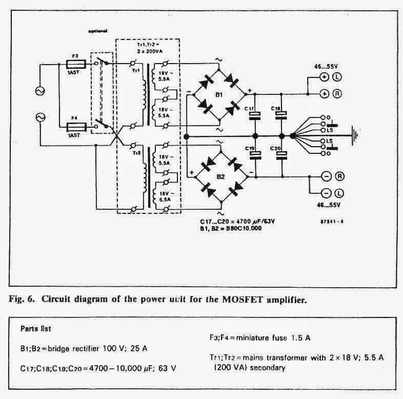
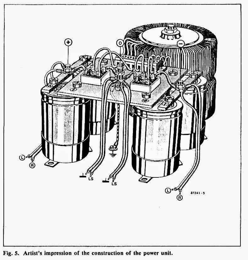
Remember the wire bridges. The power supply for the 160 watt model is shown in
Fig. 6: adjustments for the supplementary models are shown in Table 2. An artsist’s conception of its engineering is presented in
Fig. 7. As soon as the power unit is constructed, the open-circuit working voltages could possibly be checked.
The d.c. voltages needs to be not above +/- 55 V, else there is a risk that the MOSFETs would give up the goblin on initial power-on.
In case appropriate loads are obtainable, it will be, of course, advantageous that the source is examined under load restrictions. Once the power supply is realized to be Fine, the aluminium MOSFET setup is screwed directly to an appropriate heat sink.
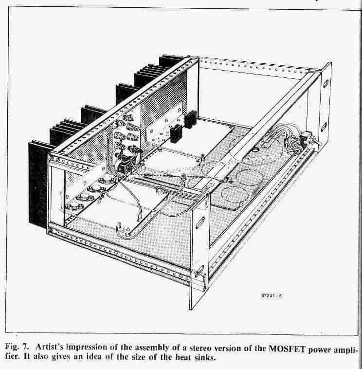
Fig. 8 presents a pretty good feel of the height and width of the heat sinks and of the finalized assortment of a stereo model of the amplifier.
For simplicity, mainly the standing of the parts of the power source is demonstrated. The places where the heat sink and the aluminium MOSFET setup (and, probably, the backside panel of the amplifier enclosure) get together ought to be assigned an effective covering of heat conducting paste. Every of the two assemblies must be screwed to the incorporated heat sink with no less than 6 M4 (4 mm) sizing screws.
The electrical wiring must stick to the guide lines in Fig. 8 faithfully.
It is advisable to start with the supply traces (heavy gauge wire). Following, establish the ground connections (star-shaped) from the power device ground to the PCBs and the output ground.
Thereupon, create the cable connections between PCBs and loudspeaker terminals as well as those between the input sockets and the PCBs. The input ground should always be hooked up solely to the ground lead on the PCB - that's all!
Calibration and testing
Rather than fuses F1 and F2, attach 10ohm, 0.25 W, resistors in their location on the PCB. Preset P2 has to be fixed completely anticlockwise, although P1 is scheduled to the center of its rotation.
The loudspeaker terminals continue being open, as well as the input should be short-circuited. Power up the mains. Should there be any kind of short-circuits in the amplifier, the 10 ohm resistors will start fuming!
If that takes place, shut off right away, identify the problem, change the resistors, and turn on the power once more.
The minute everything looks proper, hook up a voltmeter (3 V or 6 V d.c. range) across one of the 10-ohm resistors. There has to be zero voltage across it.
If you find P1 is not flipped completely anticlockwise. The voltage ought to climb while P2 is steadily changed clockwise. Set P1 for a voltage of 2 V: the current in that case could be 200 mA, i.e.: 100 mA per MOSFET. Disconnect, and change the 10-ohm resistor by the fuses.
Turn on power yet again, and check the voltage between earth and amplifier output: this certainly will be not higher than +/-20 mV. The amplifier is after that prepared for intended functionality.
A concluding point. As previously explained, the changing over guideline of the overheating security circuit has to be allocated for approximately 72.5 °C.
This can easily be determined by heating the heat sink with, e.g., with a hair dryer and assessing its heat.
Yet somehow, this may not be exactly essential: P1 could also be allowed fixed at the middle of its dial. Its situation really should only be changed if the amplifier switches off too frequently.
However, its stance should on no account be faraway from the middle location.
Courtesy: elektor.com
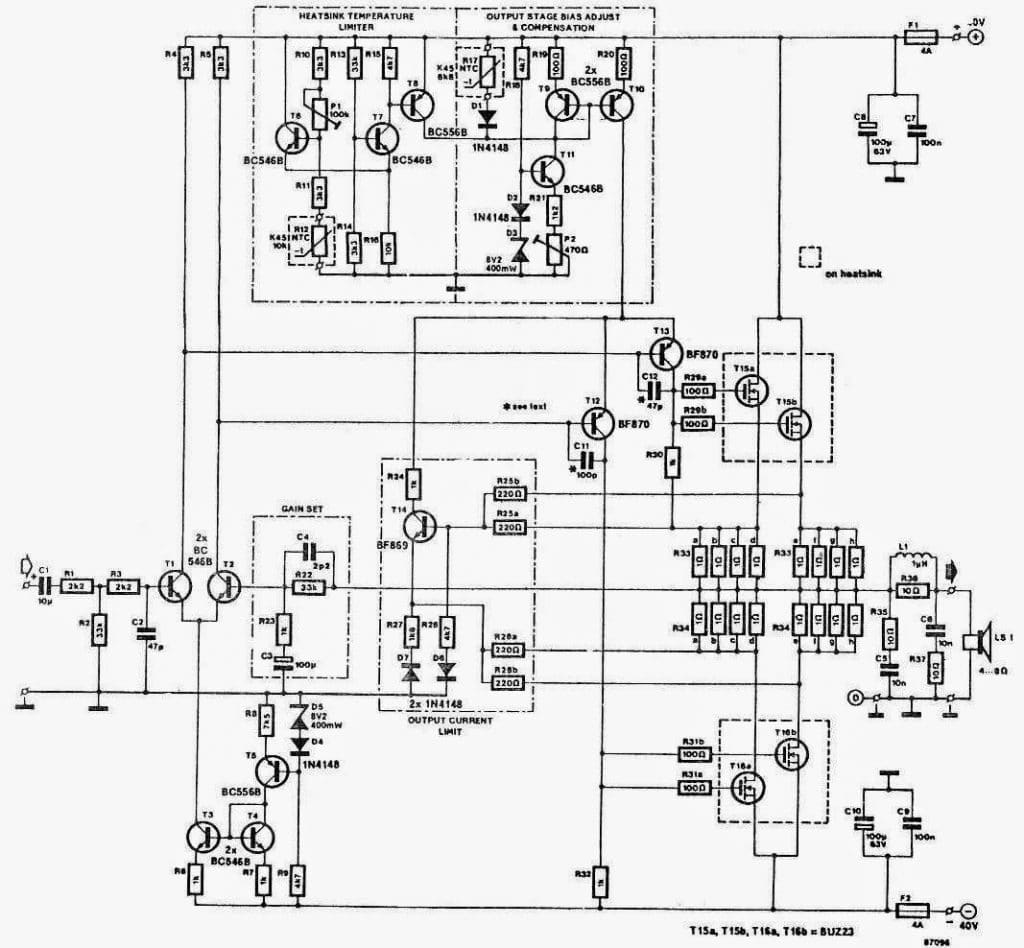
Fig:2
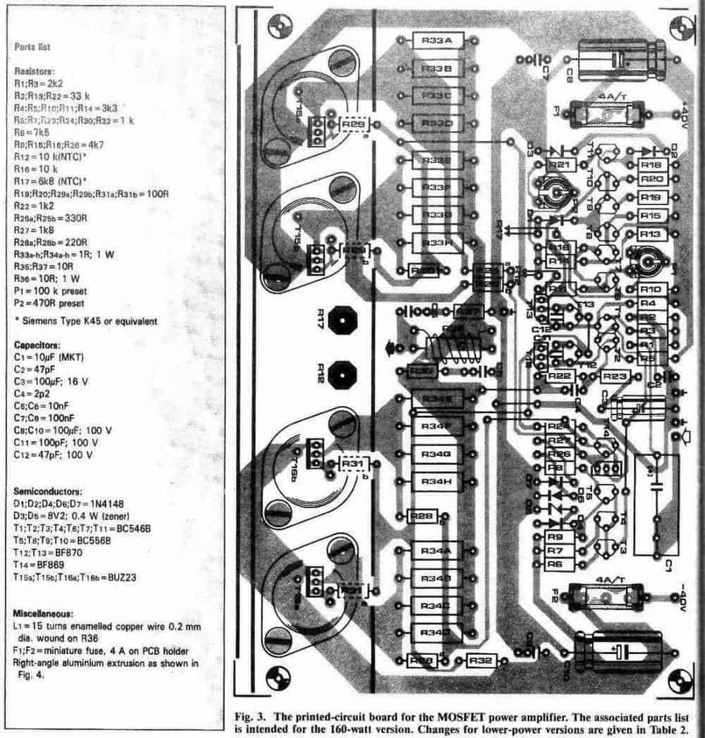
Fig:3


Comments
the power amp is built to work on ±50v to ±55v at 500w
hi sir..thank you for all the help you render making life easier sir…
sir pls I need a temperature control speaker protection circuit that switches a relay when overheating and also protects against DC in the output….
Hi MD, you can try the following circuit, it will protect your speaker from over heating….
https://www.homemade-circuits.com/wp-content/uploads/2024/08/speaker-over-heat-protector-circuit.jpg
DC protection is not required because all amplifiers already include an output blocking capacitor…
thnks sir…
is ic2a also lm334z???
Sorry for the confusion MD, IC1 is LM334…IC2 can be any op-amp
Thanks Sir, please is it possible to tweak this to produce over 100% efficiency with this voltage amplifier.
Thanks Swag.
Hi Tinu, No, that is not possible.
Good day Swag, please further explain the transformer diagram,the 2 trafos are linked together, giving one common ground and 2 sides output, won’t them cross react.
Hi Tinu,
the DCs from the two transformers are perfectly isolated through the separate bridge rectifiers, so there’s no question of any cross talks or reactions.
Thanks sir, please what is the importance of the 2 big capacitors is parallel?
Parallel capacitors increases the capacitive performance of the capacitor more effectively than using a single capacitor.
Sir, can any of this power amplifier circuits be used into 8 ohms?
yes 8 ohm speaker can be used, although the power output will decrease proportionately
Thank you Sir for your quick response. Definitively I’ll going to put one of this power amps together with my son. It will be a good quality time between us. Thank you again sir. I’ll be contacting you if we come with any questions.
You are welcome Rafael.
Hi,I have a couple of irfp260n MOSFETs lying around,can we make an audio amplifier out of them??
Hi, you can use them at the output stage of a mosfet based amplifier such as the above explained one…
Hi Swag,
Hope you’re doing well. I have a query to build an Sound System for a Mosque in our area which has total 3 floors of 500 Yards each. Do you have any schematic for this type of system?
Hi Saqib,
you can try the following circuit, it will give a good 200 watt of output sufficient for your requirement, I have tested this circuit myself, it works great!
https://www.homemade-circuits.com/how-to-make-simplest-100-watt-mosfet/
Swagatam Sir
I want to construct a temp.controlled fan controller circuit for my glass house with LCD display and temp.inputs for both max.(auto on)and min.(auto off)with LM 35 or DS 1820 and IC'S but not arduino.Please help Sir.
Hi Debarata, you can try the second circuit from the following article:
https://www.homemade-circuits.com/2016/08/incubator-temperature-controller.html
but there's no LCD for this, instead you can use the associated LEDs in the bar graph mode for getting a sequentially incrementing bar graph kind of display for the temperatures.
quiescent current DMM se set kerne ke liye keya ker na parega. mere pas jo ampli he uska output per 100v & 70v 500w.to kese set kere? over heat hoker off ho.jaraha he
…DC ampere range
…for checking on DMM, set the DMM on DC range and connect it in series with the bulbs and do the procedures as explained above.
connect 220V 10watt filament bulbs in series with both the (+) and (-) supply lines of of the amplifier.
see the glow on the lamp, and adjust the quiescent current preset until the filament is completely OFF, and there's no glow on it. This will set the minimum quiescent current for the amplifier without load.
make sure to short circuit the input terminals with ground of the amplifier, and disconnect the loudspeaker from the output.
With amplifiers does the power increase at the transistor section for example If I was to build a 1000 watt amplifier would it be possible to use a 500 watt transformer oat the power supply section but to send power to the amplifier but because of the output transistors on the amplifier I would be able to pull up to 1000 watts, question sounds stupid but I always wonder.
No that's never possible,the output power will be always a little lower than the input power.
Dear Mr.majumdar, I want to know whether the given circuit and PCB is proven to work ? If any body has made it or tried please reply. I had tried to make the MOSFET but it did not work. So I am not sure about the circuit or the correctness of given PCB. As it is the components we're were hard to get (BUZ Mosfets). But I want to try again.
Pl advice,
Thanking you in advance.
-rajit panesar
Dear Mr.Majumdar,
I want to know whether the MOSFET amplifier from Elector has been made and tested by you or some one else reading this comment. I need this information since I had tried making this amplifier while it was published in elector, but it did not work. Also the BUZ mostest are difficult to find. Any alternate MOSFET May please be suggested. Thanks in advance.
Dear Rajit,
as you can see the design is quite complex and a smallest of mistakes could prevent the circuit from working, so I personally believe that the above circuit and other similar published in elektor are all correct, tested and would definitely work, but only if it's built by an expert in the field, because such circuits will never work at the first go, there will be some hidden issues which the user will need to troubleshoot in order to succeed with the project.
you can try IRF540 for the mosfets and see how it responds.
hi Mr swagatam im looking for non contact ac tester with low volts as the current maket one reads volts at 90vac. i want to test christmas lights which is in 12v ac pls advice i saw some circuits in google but its all for 90vac lowest. pls advice sir.
Hi Steven, you can try the following circuit:
https://www.homemade-circuits.com/2011/12/how-to-make-non-contact-ac-mains-phase.html
although this was tested on 220V AC (from 2 feet distance), i believe it will work well even with 90V AC at a closer proximity
Hi swagatam sir congratulations for all amazing work please give me any circut
for agricultural fields need to protect the crops from uninvited guests like animals
i want to Active infrared barrierl [leaser ] circut diste range 100 miter or above
(my english is poor so please….)
thanks
OK I'll try to design and post it soon.
thanks for reply sir i want output alaram sound and light activation(Only night)BOTH
Thanks unknown,
what kind of output are you looking for…is it in the form of alarm sound, electric shock activation or light activation??
Pls Sir,
I need a circuit or device that can test if a sealed lead acid battery is still has any charge in it without having to short the lead with a wire.
Thanks
Setute
Setute, you can use a DMM in the 20 amp DC range and connect the prods to the battery terminals through a 2200uF capacitor….the magnitude of momentary current display on the meter screen will give an idea of the battery health….the reading will depend on the battery AH rating also