Very often we see that output coming from a microcontroller, oscillator, comparator, or PWM stage is just not strong enough for driving a power MOSFET directly, it gives signal, yes, but gate does not respond properly unless some decent current reaches there.
A MOSFET gate behaves like a small capacitor, so now unless that gate gets enough charging current and also enough discharge path, then switching stays slow, not sharp.
When the gate charges too slowly, then the MOSFET remains longer inside its linear region, and during that time it starts heating more than it should, which means power gets wasted and efficiency drops a bit, sometimes more, depending on load.
So to avoid that, we normally put one transistor driver stage in between, because direct signal line alone often does not handle gate properly.
Here we will see two simple MOSFET driver circuits, one uses two BD139 transistors, both NPN, and the other uses BD139 with BD140 in push-pull totem pole form.
Both improve gate drive strength, however the switching action is not the same, one behaves slower on one side, while the other pushes and pulls the gate more properly, so response becomes different.
Audio/Video Representation
First Circuit: Dual NPN BD139 MOSFET Driver
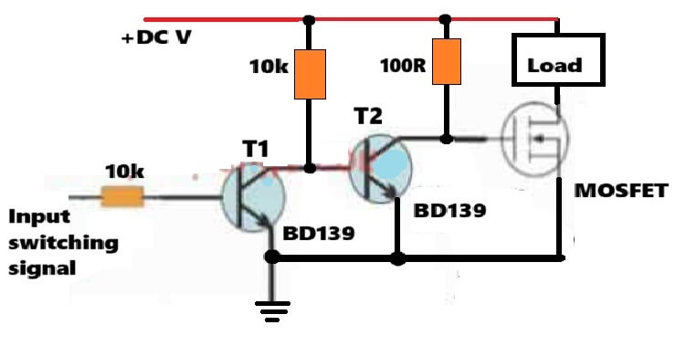
In the first design both transistors are BD139 NPN types and we first send the input switching signal through one 10k resistor into the base of transistor-1, which simply keeps the base current under limit, so the transistor does not get hit by too much drive current from the source.
The emitter of transistor-1 stays at ground but its collector goes upward through one 10k pull-up resistor to the positive supply, and that same collector point also goes straight to the base of transistor-2, so now transistor-1 is not only controlling transistor-2, it also flips the signal side,.
Now when the input goes high then transistor-1 turns ON and its collector drops almost near ground.
Since that collector point is also feeding transistor-2 base, then transistor-2 now sees low voltage there, so transistor-2 turns OFF.
Because transistor-2 collector is tied upward through another 100 ohm resistor, that point rises high, and this high level reaches the MOSFET gate, so now the MOSFET turns ON and the load starts working.
When input goes low then transistor-1 stops conducting, and its collector gets pulled high again by that 10k resistor.
That high then reaches transistor-2 base, so transistor-2 starts conducting and now its collector pulls the MOSFET gate downward toward ground.
So the MOSFET turns OFF and the load also goes inactive, simple as that, one transistor goes one side, the other follows opposite.
Important Characteristic of This Circuit
This arrangement already gives much stronger gate drive than direct logic output, because transistor-2 can push more current than the original signal source, so now the gate does not stay weak like before.
However the charging side and discharging side do not behave equal, that is where the difference comes.
Gate charging happens through a resistor, but gate discharge goes through transistor conduction, so discharge becomes faster while charging stays slower.
Since that difference is there, then this circuit fits better where switching speed is not very high, like low frequency switching, moderate PWM work, small inverter experiments and also relay replacement type circuits, where we do not need very sharp equal rise and fall every time.
Limitation
At higher switching frequencies, the gate charging path becomes relatively weak because the pull-up 100 ohm resistor limits current.
This causes slower turn-on and increases switching loss inside the MOSFET.
Second Circuit: Push-Pull Totem Pole Driver Using BD139 and BD140
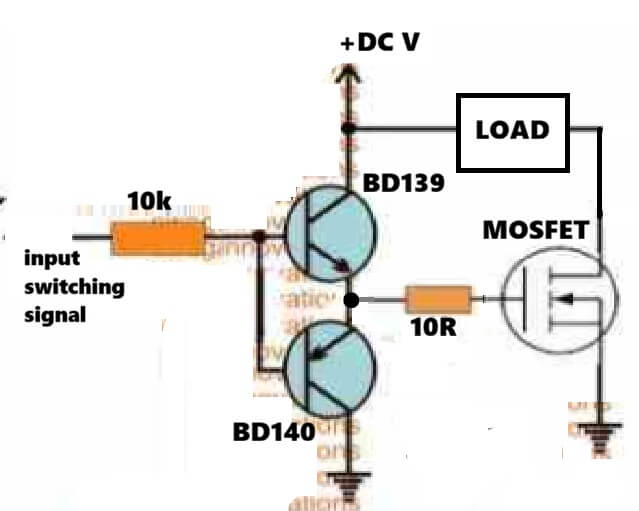
This second circuit is stronger, yep, because here both transistor sides work together, not one side only, so gate charging and gate discharge both happen better.
Here BD139 is the NPN transistor and BD140 is the PNP transistor, and we use both together which makes one push-pull stage, people also call it totem pole driver.
Now see the arrangement, input switching signal first comes through one 10k resistor, then reaches the common base point where both transistor bases join.
The collector of BD139 goes to positive supply, but the collector of BD140 goes to ground, so now both sides sit opposite and wait for input movement.
Their emitters are joined together and that common emitter point becomes the output line which is the working node from where drive comes out.
That output then goes to the MOSFET gate through 10 ohm resistor, so gate current gets controlled a little and sharp switching stays safer.
Why the 10 Ohm Gate Resistor Is Important
Even though this resistor is small, we still see it does an important job, because it positions there quietly but helps stop gate ringing, limits surge current during switching, protects the transistor pair from sudden current spikes, and moreover cuts unwanted oscillation which comes from gate wiring inductance.
How it Works
Now when input goes high, then BD139 turns ON and BD140 stays OFF.
So now BD139 pushes current into the MOSFET gate directly, which charges the gate fast, and because of that the MOSFET turns ON sharply and the load starts working without delay.
When input goes low then BD139 stops, and BD140 turns ON at that time.
BD140 then gives a quick discharge path from gate to ground, so the stored gate charge leaves fast, and therefore the MOSFET turns OFF sharply too.
The main useful thing here is that gate movement happens actively both ways, not only one side.
That means charging current is strong, and discharge current also stays strong, because both ON and OFF sides are forced by transistor action.
Since both transitions are tightly pushed, switching becomes faster and cleaner, which helps a lot when frequency rises.
So this kind of stage fits well for PWM work, inverter output side, high frequency switching, transformer driver sections, induction circuits, and also SMPS type designs, where clean gate control matters a lot.
Comparison Between the Two BJT MOSFET Driver Circuits
The first circuit is simpler, we can see that it uses only NPN transistors, so now building becomes easy, fewer parts, less trouble, and yep it works well where switching speed is not a big issue.
The second circuit however is stronger when gate movement must happen faster, because it does not only push current, but also pulls it back, so charging and discharging both happen harder.
In practical use, if switching frequency is low then the first one is often enough, no need to make things bigger than required.
But when PWM or inverter side runs faster, then the second circuit gives much better result, because gate transition becomes cleaner and quicker which helps overall switching.
Practical Transistor Selection
Although BD139 and BD140 are shown here, equivalent NPN and PNP transistor pairs can also be used.
If higher gate current is required, then stronger transistor pairs may be selected depending on the MOSFET gate charge.