In this post we will discuss two methods of designing pure sine wave inverter circuits using 555 IC based SPWM processing. In the first concept we connect the 555 processors directly with the SG3525 outputs and do the sine wave conversion directly at the MOSFET gates. In the second concept we do it externally and then use the SPWMs to chop the gates of the MOSFETs for the sine wave conversion.
Using Integrators and 555 PWM Precessors
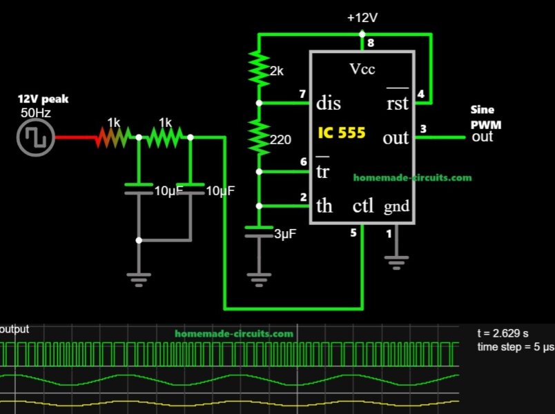
In the first diagram below we can see that the whole inverter is working in steps, first SG3525 makes square waves, then we change that square wave into a sine like wave, then we use 555 to convert that sine into SPWM, and finally we push that SPWM into MOSFET gates... The MOSFEETs now switch the transformer winding ON/OFF in accordance with the 555 SPWM sine waves causing the output 220V also to become like pure sinewave output...

SG3525 Square Wave Generation
Here the SG3525 is not used as a full PWM controller, it is only used as a stable oscillator and phase splitter, so now SG3525 makes two square waves which are exactly opposite in phase, one goes high when the other goes low, this is perfect for push pull inverter operation.
The timing resistors and capacitors set the base frequency, and dead time resistors make sure that both outputs never conduct together, so if dead time is present then MOSFETs stay safe and no shoot through happens.
At this stage the waveform is pure square wave, stable in frequency, and balanced on both outputs.
RC Integrator Sine Shaping
Now we take this square wave and pass it through RC networks made using 1k and 10uF, two stages are used so now higher harmonics get reduced more.
What actually happens is that square wave has many harmonics, RC networks act like low pass filters so the sharp edges get rounded and what remains looks like a sine wave.
This is not a mathematically perfect sine but it is good enough as a reference waveform for SPWM, and since the SG3525 frequency is stable, the phase shift caused by RC does not create serious problems.
If RC value is too high then sine becomes delayed and weak but if RC is too small then waveform remains rough, so the selected values are reasonable.
555 PWM Modulator Stage
Now comes the important block, the 555 ICs. Each 555 is running as a high frequency oscillator, usually in the range of few kHz to many kHz.
The sine wave from the RC integrator is fed into pin 5 of the 555, which is the control voltage pin.
Inside the 555, the internal ramp waveform is compared with the control voltage, so when the sine voltage is high, then PWM duty cycle becomes wide, and when sine voltage is low, then PWM duty cycle becomes narrow.
So now the output of the 555 becomes sine modulated PWM meaning pulse width follows the sine shape, this is classic analog SPWM technique and it is old but very reliable.
The 555 pwm processor and Integrator sections could be optimized as per the following Simulation results....
MOSFET Gate Drive And Power Stage
The SPWM output from each 555 goes to the MOSFET gates through 10R resistors, these resistors slow down switching slightly and prevent ringing.
IRF3205 MOSFETs are suitable for 12 V inverter because they have low Rds on and high current capability.
Each 555 drives one side of the push pull transformer primary, so when one side is active, the other is off.
If then gate drive is clean and timing is correct then transformer primary current becomes SPWM shaped.
Transformer And Output Waveform
The transformer does not pass high frequency PWM efficiently so core inductance and leakage inductance naturally filter the waveform.
Because of this filtering effect, the high frequency components get removed and the secondary voltage looks like a sine wave.
The diodes across the primary help in clamping spikes and protecting MOSFETs from inductive kickback, so now reliability improves.
Good Points In the Design
The design is fully hardware based, no microcontroller, easy to understand and easy to repair.
The signal flow is clean, square to sine to PWM to power stage so now troubleshooting becomes simple.
This type of inverter is suitable for long running systems and rural usage where simplicity matters.
Important Limitations To Understand
There is no output voltage feedback so if battery voltage rises or falls then output AC voltage will also change.
Load variation also affects output voltage because there we dont have regulation loop.
The control pin of 555 is sensitive to noise so decoupling capacitor and good grounding are very important, or else PWM jitter can happen.
Gate drive current from 555 is limited so at higher power levels switching losses can increase and MOSFETs may heat more.
Final Conclusion
So overall the inverter concept is correct, practical and proven.
The SG3525 generates stable square waves, RC networks convert them into sine reference, 555 converts sine into SPWM and MOSFETs amplify that power into the transformer.
With good layout, tuning, and optional feedback improvement, this circuit can give us clean sine like output and work reliably for long time.
Audio/Video Representation
Using Op amp based SPWM Processor and Chopping Concept
Now below next we will learn how to upgrade a standard SG3525 inverter circuit into a pure sine wave inverter using an opamp based SPWM generator, so let's understand the details through the following explanation:
How the Conversion from Squarewave to Sine wave Happens
You might be curious to know regarding what exactly happens in the process of the conversion which transforms the output into a pure sine wave suitable for all sensitive electronic loads.
It is basically done by optimizing the sharp rising and falling square wave pulses into a gently rising and falling waveform. This is executed by chopping or breaking the exiting square waves into number of uniform pieces.
In the actual sine wave, the waveform is created through an exponential rise and fall pattern where the sinusoidal wave gradually ascend and descend in the course of its cycles.
Using SPWM or Sine Pulse Width Modulation
In the proposed idea, the waveform is not executed in an exponential, rather the square waves are chopped into pieces which ultimately takes the shape of a sine wave after some filtration.
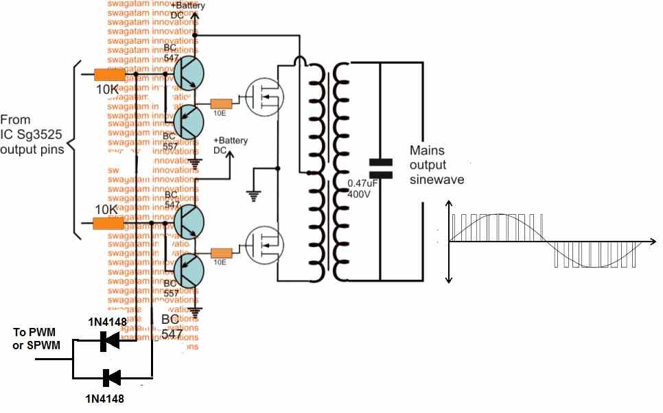
The "chopping" is done by feeding a calculated PWM to the gates of the FET via a BJT buffer stage.
A typical circuit design for converting the SG3525 waveform into a pure sine wave waveform is shown below. This design is actually an universal design which may be implemented for upgrading all square wave inverters into sine wave inverters.
Chopping the MOSFET Gate with SPWM
As may be in the above diagram, the lower two diodes are connected to a PWM feed or input, which causes the transistors to switch according to the PWM ON/OFF duty cycles.
This in turn rapidly chop the 50Hz pulses at the bases of the BC547/BC557 coming from the SG3525 output pins.
The above operation ultimately force the mosfets also to turn ON and OFF in the same pattern as the SPWM for each of the 50/60Hz cycles. This SPWM is then induced into the transformer primary by the MOSFETs, consequently producing a sine waveform at the output or the secondary side of the transformer.
If an ordinary PWM is used as I have explained below, then its frequency should be 4 times more than the base 50 or 60 Hz frequency. so that each 50/60Hz cycles are broken into 4 or 5 pieces and not more than this, which could otherwise give rise to unwanted harmonics and mosfet heating.
PWM Circuit
The PWM input feed for the above explained design can be acquired by using any standard IC 555 astable design as shown below:
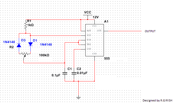
This IC 555 based PWM circuit can be used for feeding an optimized PWM to the bases of the BC547 transistors in the first design such that the output from the SG3525 inverter circuit acquires an RMS value close to mains pure sine wave waveform RMS value.
Using an SPWM
Although the above explained concept would greatly improve the square wave modified output of a typical SG3525 inverter circuit, an even better approach could be to go for an SPWM generator circuit.
In this concept the "chopping" of each of the square wave pulses is implemented through a proportionately varying PWM duty cycles rather than a fixed duty cycle.
I have already discussed how to generate SPWM using opamp, the same theory may be used for feeding the driver stage of any square wave inverter.
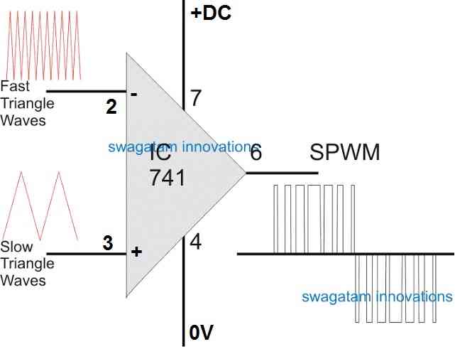
A simple circuit for generating SPWM can be seen below:
Using IC 741 for Processing SPWM
In this design we see a standard IC 741 opamp whose input pins are configured with a couple of triangle wave sources, one being much faster in frequency than the other.
The triangle waves could be manufactured from a standard IC 556 based circuit, wired as an astable and compactor, as shown below:
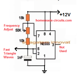
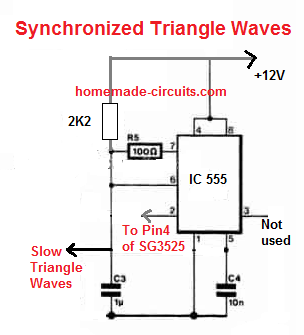
#UPDATE: The above "slow triangle waves" can be directly acquired from the Ct pin of the IC, that means you can now eliminate or ignore the above IC 555 stage for the slow triangle waves.
As can be seen in the above two images, the fast triangle waves are achieved from an ordinary IC 555 astable.
However, the slow triangle waves are acquired through an IC 555 wired like a "square wave to triangle wave generator".
The square waves or the rectangular waves are acquired from pin#4 of SG3525. This is important as it synchronizes the op amp 741 output perfectly with the 50 Hz frequency of the SG3525 circuit. This in turn creates correctly dimensioned SPWM sets across the two MOSFET channels.
When this optimized PWM is fed to the first circuit design causes the output from the transformer to produce a further improved and gentle sine waveform having properties much identical to a standard AC mains sine waveform.
However even for an SPWM, the RMS value will need to be correctly set initially in order to produce the correct voltage output at the output of the transformer.
Once implemented one can expect a real sine wave equivalent output from any SG3525 inverter design or may be from any square wave inverter model.
Finalized SG3525 Pure Sine Wave Inverter Circuit
The following diagram shows the finalized design of the pure sine wave inverter using IC SG3525 and SPWM, as per the above explanations.
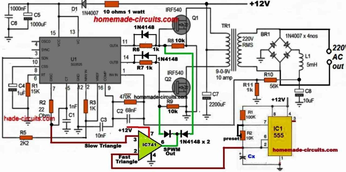
If you have any doubts regarding the above SG3525 pure sine wave inverter circuit you can feel free to express them through your comments.
A basic example design of a SG3525 oscillator stage can be seen below, this design could be integrated with our previous PWM sine wave BJT/mosfet stage for getting the required enhanced version of the SG3525 design:
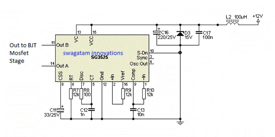
Complete circuit diagram and PCB layout for the proposed SG3525 pure sine wave inverter circuit.
PWM Modified Sine wave Inverter Circuits
Courtesy: Ainsworth Lynch
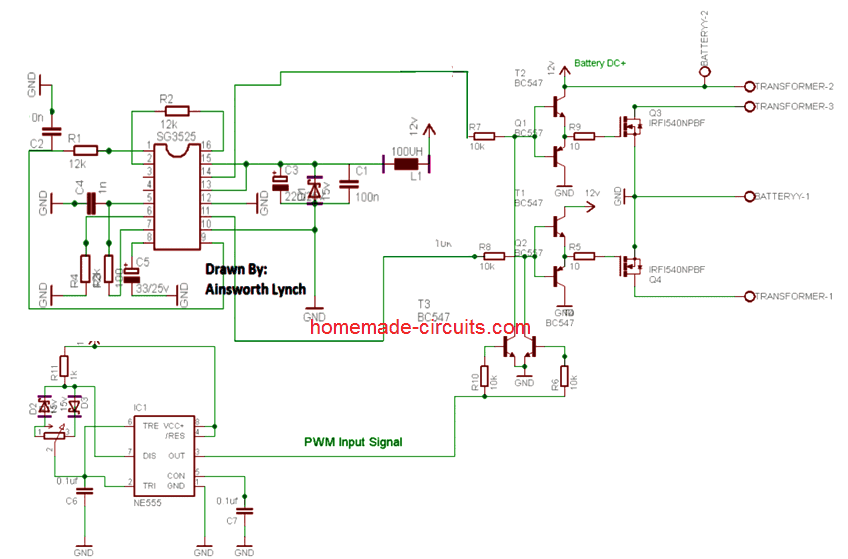
Design#3: 3kva Inverter circuit using the IC SG3525
In the previous paragraphs we have comprehensively discussed regarding how an SG3525 design could be converted into an efficient sine wave design, now let's discuss how a simple 2kva inverter circuit can be constructed using the IC SG3525, which can be easily upgraded to sine wave 10kva by increasing the battery, mosfet and the transformer specs.
The basic circuit is as per the design submitted by Mr. Anas Ahmad.
The explanation regarding the proposed SG3525 2kva inverter circuit can be understood from the following discussion:
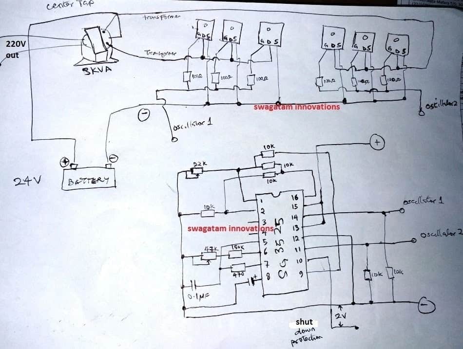
hello swagatam, i constructed the following 3kva 24V inverter modified sine wave (i used 20 mosfet with resistor attached to each, moreover i used center tap transformer and i used SG3525 for oscillator).. now i want to convert it to pure sine wave, please how can i do that?
Basic Schematic
My Reply:
Hello Anas,
first try the basic set up as explained in this SG3525 inverter article, if everything goes well, after that you can try connecting more mosfets in parallel.....
the inverter shown in the above daigram is a basic square wave design, in order to convert it to sine wave you must follow the steps I have explained below The mosfet gate/resistor ends must be configured with a BJT stage and the 555 IC PWM should be connected as indicated in the following diagram:
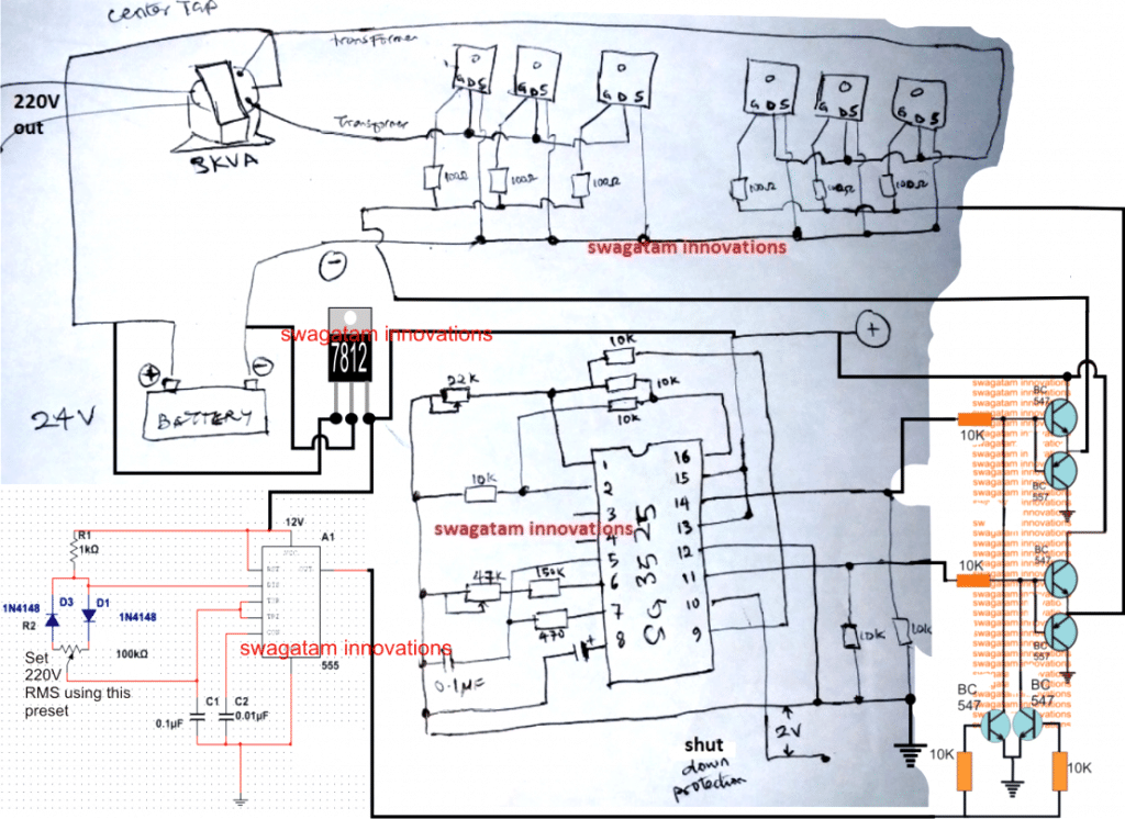
Regarding Connecting parallel mosfets
ok, i have 20 mosfet(10 on lead A, 10 on lead B), so i must attached 2 BJT to each mosfet, that's 40 BJT, and likewise i must connect only 2 BJT coming out from PWM in parallel to the 40 BJT? Sorry am novice just trying to pick up.
Answer:
No, each emitter junction of the respective BJT pair will hold 10 mosfets...therefore you will need only 4 BJTs in all....
Using BJTs as Buffers
1. ok if i may get you right, since you said 4 BJTs, 2 on lead A, 2 on lead B, THEN another 2 BJT from the output of PWM, right?
2. am using 24 volt battery hope no any modification to the BJT collector terminal to the battery?
3. i have to use variable resistor From oscillator to control the input voltage to the mosfet, but i don't know how i will go about the voltage that will go to the base of the BJT in this case, what will i do so that i want end up blow up the BJT?
Yes, NPN/PNP BJTs for the buffer stage, and two NPN with the PWM driver.
24V will not harm the BJT buffers, but make sure to use a 7812 for stepping it down to 12V for the SG3525 and the IC 555 stages.
You can use the IC 555 pot for adjusting the output voltage from the trafo and set it to 220V. remember your transformer must be rated lower than the battery voltage for getting optimum voltage at the output. if your battery is 24V you can use an 18-0-18V trafo.
Parts List
IC SG3525 Circuit
all resistors 1/4 watt 5% CFR unless otherwise specified
10K - 6nos
150K - 1no
470 ohm - 1no
presets 22K - 1no
preset 47K - 1no
Capacitors
0.1uF Ceramic - 1no
IC = SG3525
Mosfet/BJT Stage
All mosfets - IRF540 or any equivalent Gate resistors - 10 Ohms 1/4 watt (recommended)
All NPN BJTs are = BC547
All PNP BJTs are = BC557
Base Resistors are all 10K - 4nos
IC 555 PWM Stage
1K = 1no 100K pot - 1no
1N4148 Diode = 2nos
Capacitors 0.1uF Ceramic - 1no
10nF Ceramic - 1no
Miscellaneous IC 7812 - 1no
Battery - 12V 0r 24V 100AH Transformer as per specs.
A Simpler Alternative
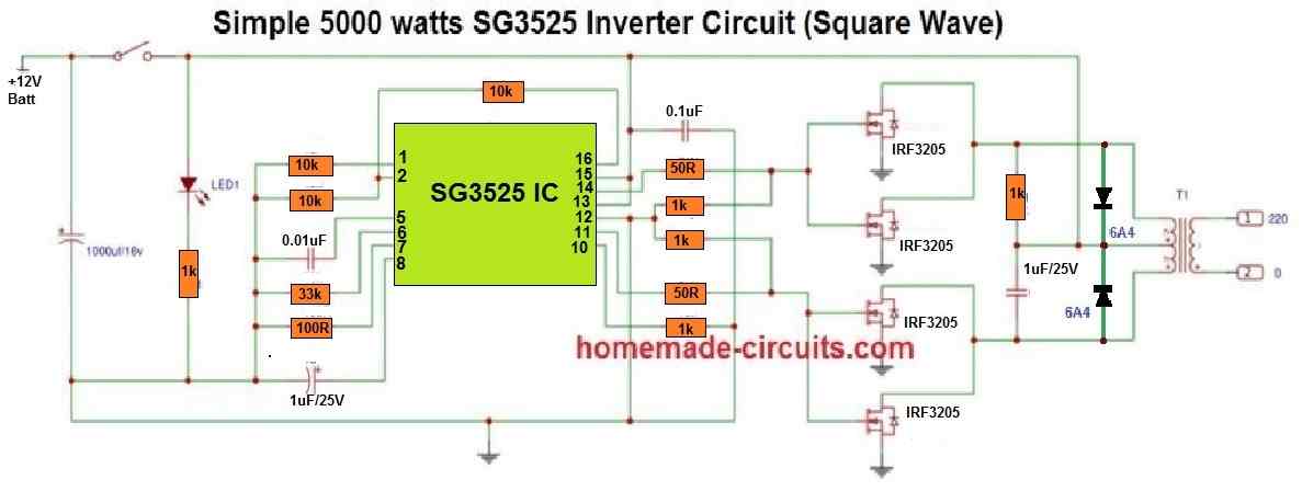


Questions & Answers
Sir i cant make any electronics circuits because of i cant identify Emitter Base and Collector properly. i am using Digital multi miter . Sir please help me
Refer to datasheets of the concerned devices and you will be able to find the pinout arrangement instantly
Thanks for the lecture I will try and see the difference thank you very much for sharing.
Hi,
First of all thank you for publishing that much of hard work free for any body to use. Also could you please tell me how you limit or achieve 4-5 pulses in each 50Hz cycle. Does it happen automatically once you connect BC547 to SG3525. Thanks,
Hi, Thanks, it is initiated when PWM is fed at the bases of the two BC547 transistors shown at the bottom of the first circuit.
The PWMs can be generated using the recommended circuits using IC 741, IC 555
Dear Mr. SWAGATAM MAJUMDAR
First of all, I would like to thank you for your dedication to help others.
Thanks for publishing the modified sine wave inverter SG3525. Some days back you published a modified sine wave project with TL494. I wish to assemble one. Could you please suggest me, which one is better with features to assemble for my home? I need an inverter with capacity of 500 to 1000watt.
Thank you, Benjamin
Thank you Benjamin,
both the ICs are significantly similar with their working specifications and features so it doesn't make much of a difference as far as performance is concerned. You can try the one which is more suitable to you…
the power output will depend on the mosfet specs and the battery AH rating
Dear Mr. SWAGATAM MAJUMDAR
Good morning and thank you for your prompt reply. I shall assemble one of the two circuits and reply you. GOD Bless you.
With regards, Benjamin
You are welcome Benjamin!
hello swag…thanks for your time and effort you take to answer questions and designs, i would like to ask this ..can the arduino be used to generate the oscillation to drive the mosfets and the pmw to feed the two BC547 ?
thanks solomon,
according to me, an Arduino can be programmed and used for generating the basic mosfet oscillations and also the PWM oscillations together from its respective pinouts.
In the ic555 circuit what is the function of the pot and what single resistor will be used in place of it for generating 4 times the base frequency? and also will i eliminate the feedback feature of the sg3525 using a 6-0-6 500ma transformer 3.if i want to add more mosfet in parallel will i use seperate 50k resistor at it's gate 4.if i build this circuit will it produce a mains ac similar waveform that can get rid of the humming of inductive loads like fan when connected to modified sinewave? thank you.
the pot is used for setting up the PWM for the inverter, and it cannot be replaced with a single resistor since it needs to be precisely adjusted for fixing the RMS value.
the fixed resistor determines the frequency
yes the feed back mess can be eliminated if the above explained method is employed, but make sure the all the circuits are supplied from a fixed voltage source using 7812 IC.
parallel mosfets can be added without any modifications.
with some filtration at the output the results could be quite similar to pure sinewave
Grertingt Lord am an amateur and need to ride the full vircuit diagran with SG 3525, IC 555 and transistors BC 547, BC 557 with list of components. Thank you
Greetings Lord am an amateur and need to ride the full circuit diagram with Sg 3525, IC 555 and the list of components. Thank you
If possible I'll try to upadte the complete design soon…
thank you sir swagatam for the cooperation that has always been with us. I hope the entire circuit when you can
Thanks Fransisco, I have updated the basic SG3525 oscillator circuit in the article, I hope now you will able to do the remaining integrations which is not difficult.
…if you have problems, let me know about it…
Hi Mr swagatam,
I really appreciate your grate jobs and ideas shares with everyone. MORE POWER TO YOUR ELBOW AND GOD WILL BLESS YOU SIR.
I've done many of your design and everything works perfect.
I want to try this as well and I will need you to guide me through if any challenge. once I finish I will share
It's my pleasure Basit. I am glad my circuits are serving the purpose for you.
I wish you all the best with this project….
Thanks
Many thanks for your response,
Can I use bc337 in place of bc557? I'm working on the circuit now
BC337 is NPN, whereas BC557 is PNP
Many thanks, I later find some 557 in one of design that I'm not using again.
I have two questions
1. Can I use 50k preset in place of 100k preset?
2. Can I use bc337 in place of bc547 aside need two more to complete the circuit and I can't get it around where I stay.
50k preset will do.
BC337 will work instead of bC547
greeting Mr. Swagatam I have some questions about the circuit 3525, I found the coil L2 100uH, I can do, and as frequency and voltage will be regulated and if you apply the 12 vol directly to the 3525 and 555. See you later.
L2 is actually not crucial you can eliminate it if you wish to…
using a 7812 could be included for ensuring a stabilized output, although this too might be not crucial…
I just saw this post I havent been here for some time, in the past I normally asked you for pcb of the circuits you make but it would normally be a case that your too busy. I have been doing some practice over the last couple months and I am now successful in building designing the pcb's and also making m own boards, I know im not as good as the professionals but for the simple circuits I build they work well for me.
I was just reading this article and was trying to put everthing together so I could make a pcb but I think I am not understanding something, ouu uploaded a basic design with the 3525, I am now wondering where should I send 2 output pins on the 3525 to:
1) An opamp?
2) the same bjt stage you have?
or would I need to make 2 triangle oscialator circuits to feed 2 opamps then send the outputs to the base on the bjt section of the inverter and also connect the output from the 3525 to the base of the bjt's also.
1) it's clearly indicated that the 3525 outputs are supposed to join with the "BJT/mosfet stage"….meaning with the two 10k resistors at the bases of the BJTs…
the opamp and triangle wave stages are associated with PWM generation.
I read it over just now I understand I can use the basic 3525 diagram and the bjt output stage and also feed the pwm input to the pwm input section on the bjt stage.
What I dont understand is the SPWM, I understand the concept just dont know the frequencies that I should feed the opamp with, how high and how low should the frequencies be by guessing I would make the fast one 200hz and the slow one 50hz my expected output is 50hz at the inverter's output.
yes 50 and 200Hz could be tried…
I just made a drawing.
https://drive.google.com/file/d/0B0N-CQJdWSP0SjViRzd1U3psbXc/view?usp=sharing
It looks good, if possible could you please connect the 555 pot center lead with pin2/6, and send it back so that I can publish it here….
https://drive.google.com/drive/folders/0B0N-CQJdWSP0UmlyUlItMV8xeTA?usp=sharing
this contains a pcb I did of the drawing also.
OK great, thanks so much, I'll update it soon in the above article!!
THE BJT STAGE BC547/BC557 MUST BE AS CLOSE AS POSSIBLE TO THE MOSFET GATE, MAKE SURE YOU RECTIFY THIS ISSUE IN YOUR PCB DESIGN
since the SPWM method is better I would like to draft up the circuit for that also but I am having probs finding triangle wave circuits to match the 50hz and 200hz output I need at the correct voltage which should be 5v I assume.
You could help me out with that I would go through your page and do some drawings of the tested circuits but i'm not sure of all those you tested, you could send me some links of circuits you dont have time to draw up and I would do them and some pcb also if you like.
a 555 IC astable circuit could be used for obtaining reasonably good triangle waves, it could be extracted across the timing capacitor of the astable.
two such circuits could be built for developing the slow/fast triangle waves and integrated with the opamp inputs
5V may not be critical, although a 7V supply for the 555 ICs would enable you to get 5V triangle waves…
Also I found this just now that you made and it seems to be a good circuit, was it tested?
https://www.homemade-circuits.com/2013/01/modified-sine-wave-inverter-circuit.html
Would any modifications need to be done to this for the waveform to run sensitive electronics?
a simple LC network at the output of the transformer would help to neutralize the harmonics and improve the waveform, although this may not be entirely critical
Ok then ill test that version of the inverter since it has so much features.
https://www.homemade-circuits.com/2013/01/modified-sine-wave-inverter-circuit.html
I hope it works well, ill make a pcb for it also.
I would like to add the LC network, commonly I would see 0.1uf 400v not sure what value inductor to use.
sorry, I think I misunderstood the link,,,,actually it is just an ordinary sg3525 design, and the features are nothing significant, the output will be crude modified square wave, not good for sensitive electronics, and it cannot be improved using LC network without huge losses.
actually I thought you were referring t this link
https://www.homemade-circuits.com/2013/10/modified-sine-wave-inverter-circuit.html
Oh no, I was refering to the sg3525 circuit with protection features, so I guess I can't build that one then.
Which circuit would you recommend me to build that has the best sine wave.
the above explained looks the most appropriate one….and can be further enhanced by adding an automatic battery charger….which is not difficult.
When you say above are you talking about the one in this article
Or
This
https://www.homemade-circuits.com/2013/10/modified-sine-wave-inverter-circuit.html
The one which is published on this page, because the linked one is not a pure sinewave.
I'll just add the battery charger circuit to the drawing, do you have any schematic you recommend.
you can probably try the second design from this article
https://www.homemade-circuits.com/2011/12/how-to-make-simple-low-battery-voltage.html
I thought you said battery charger circuit… Thats a low battery cut off circuit… But it's still handy I'll include it also.