The explained circuit in this article is probably the simplest and the cheapest, since it employs minimum number of components and the making of the circuit is very straightforward.
Circuit Operation
Generally SMPS topology involves some fixed standard stages and criteria. Thgey may be listed in the following manner:
The first stage which is the input stage incorporates an obvious mains rectifiers stage, followed a few important protection components.
The above protection components may be in the form of an MOV , or an NTC or both of these for suppressing high voltage transients.
The next stage involves a mosfet based IC in conjunction with the primary of a small transformer for generating the required oscillations.
The IC is normally a state-of -the-art chip having many in built features and abilities.
Further on the secondary of the transformer is clamped with the mosfet IC through a optocoupler which takes the responsibility of controlling the output voltage to a predetermined fixed level.
However the proposed circuit of a cheapest SMPS circuit is rather free from all these complications and employs a very simple configuration.
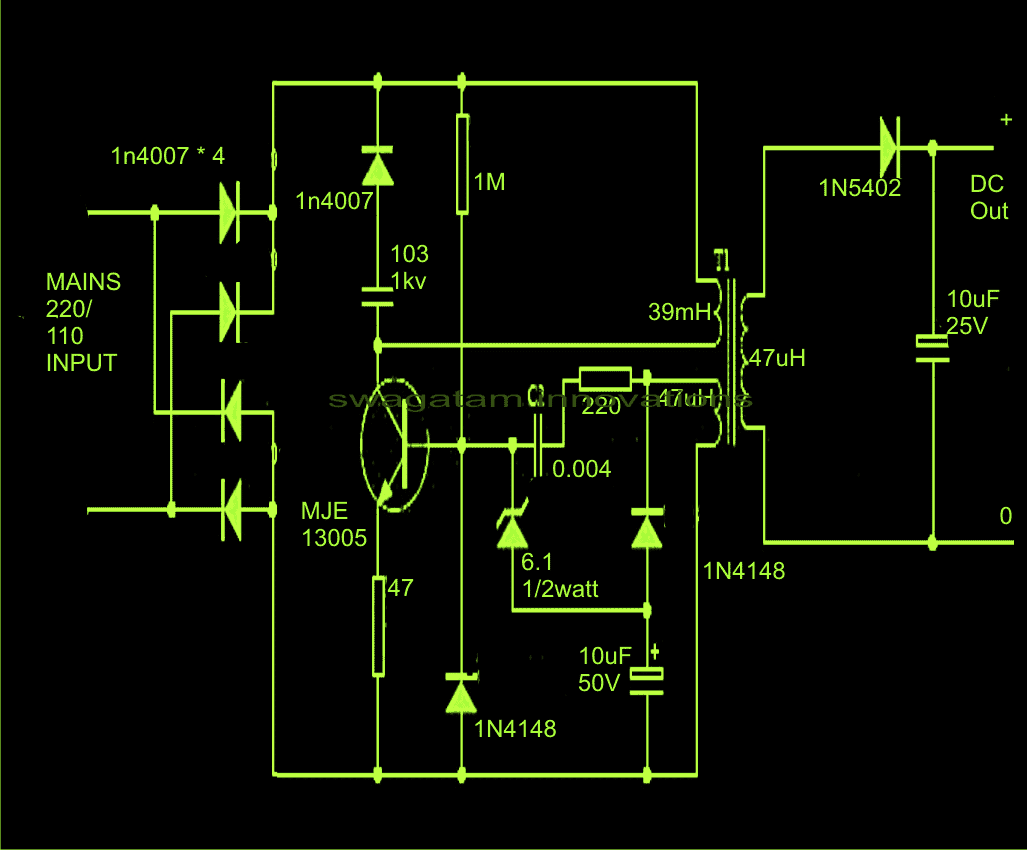
The input does not involve any protection, which is rather replaced with the snubber network around the transistor. Moreover the rugged MJE13055 is assumably strong enough to take on most the situations.
The two winding on the primary side are so arranged that on switch ON the circuit immediately starts oscillating at around 100 kHz.
The secondary winding typically decides the output voltage and here no optos or zeners are introduced for the sake of simplicity.
Having said that, the circuit may be considered quite crude and therefore in some way might be vulnerable at some point of time in the long run.
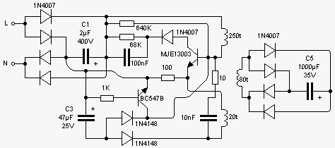
Here's another identical simple 220V SMPS circuit design you would like to investigate:


Questions & Answers
Hi Kumar,
I am sorry, I don't have the exact specifications for the transformer
In this circuit Please tell me which Component you used for high frequency switching?
the transistor and the associated components.
don't use 1N series at the output such diodes used for Low frequency rectification….u have to use fast recovery diode like UF5402(ultra fast diodes)…switching frequency of smps is in terms of kHz..mail me if you want efficient and cheap smps circuit design using BJT and mosfets..arspc8@gmail.com
can you explain the working please… i thought that the reservoir cap shud be between the ground and vcc of the primary.(hi voltage section i mean).. but here its btween the vcc and the transistor… :/
a filter capacitor may be added after the bridge, the capacitor you are referring to has a different function and is also crucial.
sir i want 24 volt 1 amp ckt in above ckt some suggestion plz..
thnks
Khodal, the above designs are not confirmed ones, instead you can try the following , but you will need to make a PCB for this:
https://www.homemade-circuits.com/2013/10/12v-24v-1-amp-mosfet-smps-circuit.html
Hi,regards.i m designing a 5v 1amp smps can u pls help me to get some idea.i want to charge samsung phone.i opened a samsung charger it consist of 13003 transistor and one 5 pin smd very small part to drive 13003.it marked rf27.in another charger it marked in30 and another one marked in70.can u pls help me to make a fast charger
Hi, I could not find any info regarding the devices in30, in70, so can't suggest much, rather you could try the following design for getting identical results:
https://www.homemade-circuits.com/2014/02/220v-smps-cell-phone-charger-circuit.html
Hello sir,
I hav noticed the 2nd schema, that it has a bridge rectifier both in input and output, it is in wrong configuration, and also in the collector of the transistor, the diode is reversed biased. Therefore this circuit wont work,
Sorry, just trying to help.
Hello khema, thanks for pointing it out, both the circuits were taken from some other site, these are not verified by me….yes the bridge configuration looks in the opposite direction for the second diagram, not sure why it's been configured in that way, I found it in one of the forums.
can you please give me the detail of transformer
can you please give the detail of transformer winding.
you can make it with the help of the inductance values given in the diagram…
Hi I am Khurram Mateen kindly send me winding data
Sir, i want to make smps with +12V, gnd & -12V. Is that possible? & if so, how to build the circuit? Plz provide me the circuit diagram…
Regards,
Mandar
Mandar, you can try extracting a center tap out from the secondary winding and get the required dual voltages .
Thank you sir..
what is the output of above circuit, can be arjusted for 5v, 9v and 12v
yes you can do it by using 78XX regulator ICs
Hi Swagatam,
I have a query regarding switching frequency..how can we select or calculate the freq. in flyback topology (upto 100W ) SMPS? I mean to say, in above ckt. which component is used for generating the switching freq.?
Hi Maddy, i can't suggest the formula immediately since I have not yet investigated the circuit deeply… but it's the base capacitor/resistor and the 47uH winding which are basically responsible for the frequency value..changing the value of any or all of these elements could cause variations in the frequency….
Can u tell me, how to design transformer for smps?
How many turns are needed for primary and secondary? And can i use transformer which used in phone charger directly?
turn numbers are shown in the second diagram, click to enlarge it.
no you cannot use the phone charger trafo directly.
Dear sir the output is not isolated form the main if we want to isolate secondary using pc 817 how will we connect it with feedback winding and secondary winding ???
Sheraz, the secondary is perfectly isolated from the primary….do you mean the primary is not linked to secondary for output control? you can do it by referring to other similar SMPS designs and by replicating the opto section
thanks sir. I have design an SMPS circuit for 12V, 2A as the design above you referred. but one problem with the output is that the output change with
changing load and the 2nd is that the output current of the transformer is not 2A but is less than it. i have used N0 = 84T(28SWG) for primary, N1 = 12T(28SWG) for feedback and N2 = 13T(25SWG) for winding the transformer. how can i get the required 12V, 2A with the above design?
Sheraz, current can be improved by using bifilar winding method..in this method instead of a single thick wire, many thin wires are wound together compactly. this allows better and efficient magnetic and current absorption…so you can also try this. instead of using single wire, use many thinner wires together and wind them tightly with the same turn numbers.
I made the circuit of MJE13005. but the transistor is heated up in no load condition and after 10 min transistor burns out and the also some other component like rectfier etc are also damaged but the out voltage at starting time is arround 13 volt
OK how can I help you?????
Please tell me the unit of 0.004 capacitor
It is uF, microFarad.
can i charge 6 volt battery from this circuit
you can by adjusting the output to 7V
thank you sir
I constructed a phone charger but it is draining my battery instead of charging it. What do I do sir
Which circuit did you build? what is your battery specs? where did you connect the battery? how much voltage are you getting at the output?
I got the circuit on the YouTube. It has a transformerless power supply having 7805 regulator. I was having 4-5v.
I want to charge Infinix note4 android phone. It shows charging but rather draining my battery.
Thanks for your feedback sir
Vaayem, is it an SMPS design or a capacitor based deign? Capacitor based design can be dangerous for the battery, phone and the user itself…It is strange that your phone is accepting the charge but not charging? Instead of trying a modified charger why not use a regular phone charger which would also guarantee a safe charging for the phone?
Thanks sir, as a beginner, l love electronics and I love building circuits that I see if they can work. Sorry, I don’t know the meaning of SMPS and the difference between capacitor based circuits. Please sir, help me. I love building circuits but know how to go about it. Like how to connect a transistor that it will amplify current. Please is there any practical hand book u can refer me to?
No Problem Vayem, you can ask your questions here, I’ll try to solve them. SMPS normally has a small transformer and is mostly isolated from mains AC and has higher current output, while capacitive power supply uses only a high voltage capacitor and no transformer, but it is non-isolated from mains therefore dangerous to touch and is low current type…
for knowing how to use transistors you can read the following post:
https://www.homemade-circuits.com/how-to-understand-and-use-transistors/
Oba tie diódové mostíky, aj vstupný aj na výstupe robia čistý skrat. Nie?
Hi
I am from Iran
please give me the detail of transformer (T1)
Hi, it is given in the diagram, use any standard E19 ferrite cores
HI,
Can we replace the MJE13005 transistor with a N-channel MOSFET ? What changes are required in the circuit for proper operation with MOSFET ?
Hi, I am not sure about it, since SMPS circuits are critical circuits and work with precise calculations.
MJE13005 is rated for 400 Volt VCEO, at 250VAC the rectified voltage will be 250* sq rt of 2 , that will be around 350VDC, on top of that the flyback reflected voltage plus spikes will cause it to go beyond 400VDC.
will this transistor sustain this?
The mains AC is 220 V not 250V and the peak is maximum 320 V..the basic spike protections are included in the design
polarity of some rectifires most change.pls cheak it again. thanks.
Dear sir,
Recently I came across the 2nd circuit involving 13003. The condition was with one zener burned out (presume that it was 1N 4148). But I changed it with some 8-10 V rating. Didnt bother to check the circuit due ignorance. Now the output is 7V (no load) instead of 5V.
Does the value of zener decide on the output voltage?
Hello Manoj, a 1N4148 should be replaced with a 1N4148 only, if you use a zener diode instead, the it can create unpredictable results or a difference in the output voltage.
Dear Sir,
I required SMPS which can work for 24volt and 2.5a current .
Regards
Hello Kush,
you can modify the following design according to your needs:
https://www.homemade-circuits.com/smps-2-x-50v-350w-circuit-for-audio/
your bridge rectifier is wrongly placed
Please explain what is wrong in it, I cannot see anything wrong in the bridge rectifier?
sir,
I have a micro-controller project.
I get supply from 3 phase AC (415VAC).
How to design simple SMPS (isolated one) to power the the micro-controller?
Micro-controller needs 5VDC.
Even if smps output is 12V, I will use some or other DC-DC converter.
Issues is how to get 415VAC to 12VDC in smps.
Hi Prabhu,
Getting a regular SMPS to work with a 415 VAC looks difficult. All the circuits which I have are designed to work with a maximum of around 360V peak or 290V RMS.
However you can get the 5V DC from a transformerless power supply, although this circuit may have floating non-isolated AC on it which can be dangerous to touch in powered condition.
Thank you sir.
I explored the transformer-less supply earlier. I want to avoid them since they don’t provide galvanic isolation.
There are already SMPS IC like LNK3694P/G (from the company Power Integrations), they have MOSFET that can support peak produced by 484 VAC (after rectification).
On other hand, I wanted to build a simple smps with a discrete MOSFET that can have switching capacity of 600VDC (415VAC * 1.41). If I use flyback transformer to switch primary side and get feedback from secondary side zener through opto-isolator.
Can you please tell me if it works.
Right now, I am using, an 415VAC to 12VAC transformer, which is bulky for me. I am notable to use standard smps board that are available in market as all of them were for 230VAC. I am not worried about efficiency of my smps. I want just galvanic isolation, a little power (3W to 5W). Please share your thoughts.
Hi Prabhu,
Yes, you can use flyback topology with feedback to build an SMPS with an input range of 600 V.
However, you will have to design the flyback transformer correctly, that’s the big challenge.