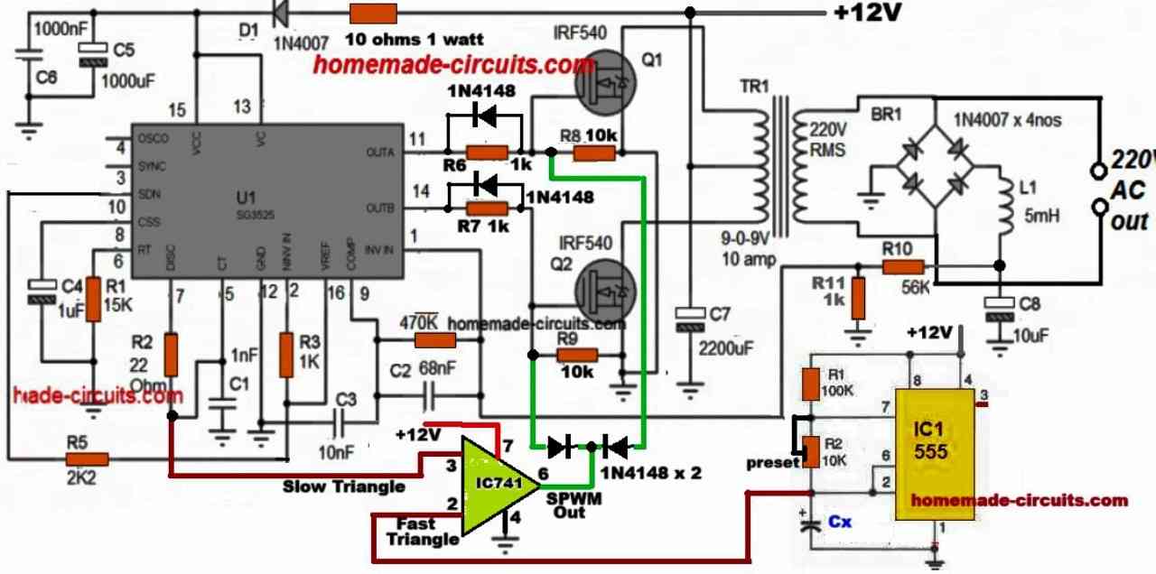
In the following post I have explained a pure sine wave inverter circuit using the IC 556 which forms the main sine wave processor device in the circuit.
How it Works
The presented design actually produces a modified sine wave output, but the waveform is highly processed and constitutes an exact equivalent of a sinusoidal waveform.
A single IC 556 forms the heart of the circuit and is responsible for manufacturing the required PWM controlled modified sine output waveform.
One half of the IC on the left is configured as a 200Hz frequency generator, this frequency is used for providing the required square wave clocks to the preceding monostable which is formed by wiring up the other half of the 556 IC.
The clocks are received from pin#5 and applied to pin#8 of the IC. The right hand side section of the IC does the actual processing of the above square wave by comparing it to the triangular waves applied at its pin#11.
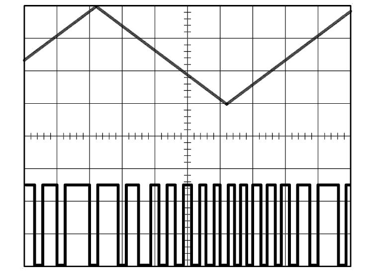
The result is an output at pin#9 which is a PWM, varying in accordance with the amplitude of the triangular waveform.
Ideally the triangular waves can be replaced with a sine waveform, however since triangular waves are easier to generate, and also appropriately replaces the sine counterpart, its been employed here.
R1, R2, C1 should be appropriately selected so that pin#5 produces a 50% duty cycle, 200 Hz frequency.
The 200 Hz is not critical here, however it becomes critical for the IC 4017 stage and that's why it's been selected to that value.
The modified sine wave PWM generated by the IC556 is next applied to the switching stage comprising the IC 4017 and the relevant output mosfet devices. Let's see how it's done.
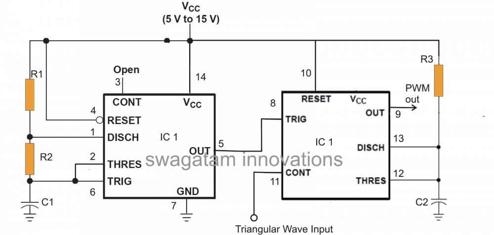
Parts List
IC1 = 556
R1,R2,C1 = select to generate 50% duty cycle
R3 = 1K
C2 = 10pF.
The output stage
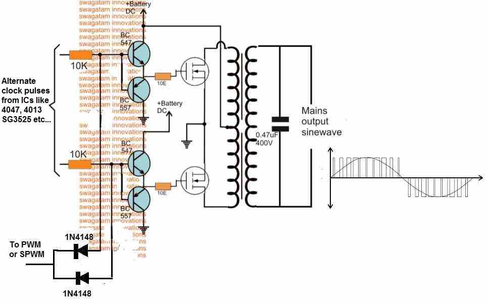
The diagram given below shows the output stage configuration where the IC 4017 takes the center stage. Basically its function is to switch the driver transistors alternately so that the connected mosfets also conduct in tandem for inducing the required mains AC output into the transformer.
The IC receives the clock pulses from the above explained 556 circuit (pin#5/8) and its outputs sequence across the connected transistors alternately as discussed above.
Until here the circuit behaves like an ordinary square wave inverter, however the introduction of D1/D2 with the pin#9 of the 556 transforms the circuit into a full fledged pure sine wave inverter.
As can be seen, the common cathodes of D1/D2 are integrated with the processed PWM pulses from the above 556 stage, this forces D/D2 to conduct only during the negative pulses from the generated PWM blocks.
It simply means that when D1/D2 are forward biased, T1 and T2 are inhibited from conducting since their gates become grounded through D1/D2 into pin#9 of the IC 556, which make the mosfets respond exactly to the PWM pattern.
The above process generates an output across the transformer secondary that's perfectly chopped and processed and equivalent to a sine waveform.
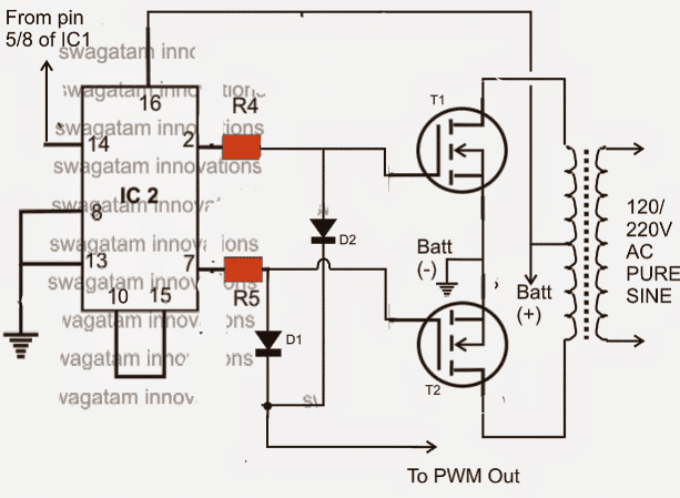
Parts List
IC2 = 4017
all resistors are 1K
D1,D2 = 1N4148
T1,T2 = IRF540n
Transformer should be also appropriately rated as per the requirement.
The Triangular Wave Generator Circuit
The entire modified sine PWM waveform construction and implementation is dependent on the fed triangular waves at pin#11 of the IC556, therefore a triangle wave generator circuit becomes crucial and imperative.
However there are many types circuits that will provide you with the required waveform inputs, the following is one of them which incorporates yet another IC555 and is pretty simple to configure.
The output from the below given circuit must be fed to pin#11 of the IC556 for enabling the proposed sine wave inverter functioning.
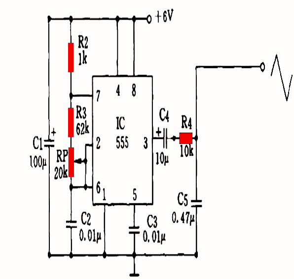
DESIGNED BY "SWAGATAM"
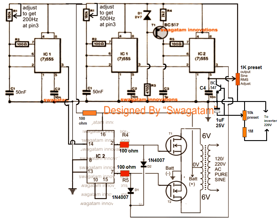
A simpler alternative to the above design is shown below, the configuration would produce same results as explained above:



Questions & Answers
thanks! this circuit will work only with center tapped trafos.
you will have to try it practically for confirming!
Thanks for ur reply sir,
At the last in above article u had posted a circuit having two (7)555ic and one 4017ic.
Is 555ic and (7)555ic has some difference in their working.
I had read some where that 7555ic has a diffrent packaging (cmos) type.can i use normal ne555 ic for above circuit
Thanks
Thanks for ur reply sir,
At the last in above article u had posted a circuit having two (7)555ic and one 4017ic.
Is 555ic and (7)555ic has some difference in their working.
I had read some where that 7555ic has a diffrent packaging (cmos) type.can i use normal ne555 ic for above circuit
Thanks
7555 consumes less current and its output is more accurate than the analogue IC555, but IC555 is able to output 200mA current which the cmos counterpart cannot….so according to me IC555 is much better than (7)555, however it largely depends on the specific application, which one suits it better.
Hi Sir,
first I want to express my respect to you, answering all the questions here.
My Name is Michael. I only want to ask a Special question……is it possible to immitate a tapped tranformer, with 2 equal resistors connected in series, which to connect both parallel to trafo to get a middle Point ? Only a thought….might be a weired one 🙂
Hi Michael,
no that will not work, because the voltage has to pass through the winding in a push pull manner in order to generate the output voltage.
Thanks for ur reply sir
So will u suggest me to use ic555 instead of ic7555 for above circuit u had discussed at end of above article.
Some more doubt i want to clear it with u
#can i use 473 instead of 50 nf capacitor.
#can 2.7v zenner will replaced with 3 v zenner
both types will work, you can use 555 or 7(555) doesn't make any difference.
473 = 47000pF = 47nF, so that's fine, you can use it.
3V zener will be ok!
Thanks for ur reply sir
At last ,there is no any Preset used in above circuit so this circuit is fixed to produce 50hz 220v at output(approx).
which mosfet i had to use and how much on each channel for 750watt trafo
(I had couple of irfp250, urfz44,irf540,irf54n06)
Thanks
You have made a good point, the last circuit is actually not set for producing 50Hz, IC1 parts will need to be changed for setting up this frequency. I'll do it soon.
Also I have added a RMS correction preset to the last circuit, I hope you have seen it.
you can use single mosfets IRf540 for each channel as shown
ok.. sir can u try the above circuit practically in small scale(in your free time) ??
we can istall visual analyser softeware in pc , den we can use pc as oscillocsope (20hz to 20khz) .. input is mic input in sound card , appropriate strobe must prepared , use o.1u capacitor , 1M ohm resistor in serias with phase for 220 v ..
NO two or more gates of mosfets can be directly connected , if we do so mosfet gets blow off, we must connect each through 47ohm resistor..
I have simplified the circuit to a great extent in the last diagram, you can try it.
hi dear swagatam can you please tell us which type of capacitiors used in all digram whether they are porcelain or ceramic.since while buying componenet they ask me which type capacitior you want.is there major change in result if i buy wrong type capacitior.
I answered this in G+
yes it can be done by using input voltages upto 60/100v and by using transformer/mosfets capable of handling 2000 watts of power
Hi Robin,
It just a constant current configuration so that the IC2 does not get affected with supply voltage variations and current up-downs.
It is not necessary, you can remove the zener, the 470 resistor, and the transistor and just connect the positive resistor to the IC pins directly
…it is not necessary if the supply is constant.
Hi Swagatam,
I have gone through several inverter circuits in this blog and i wish to make one of my own. I have tried to make inverter in the past but i faced one major problem of the output transformer. I have confusion regarding this matter. Is there anything called "Inverter Transformer" of particular rating? I asked many but none of them gave me a suitable answer. Can i get it readymade ? Do i have to manufacture of my own? It will be extremely helpful for me if you kindly clear my confusion.
Hi Arnab,
There's nothing called "inverter transformer" you can use any ordinary transformer having one side winding matching the battery voltage while the other side winding corresponding to 220V, that's all is required….current rating of the transformer will correspond to the load that needs to be operated, higher rating would allow higher loads and vice versa.
thank u very much i was tooo much confused that how to design inverter bt nw i got idea
bt which transformer to be use ???
transformer should be ideally a 9-0-9V and wattage as per load requirements.
swagatam you are great i love every page of your articles
thank you ibitoye!
Great circuit, however I read somewhere that it's always good practice to put a rather large capacitor on the primary transformer stage so as to avoid "dirty" AC. But you didn't include it ? Also, you don't explain, really, how a PWM waveform is somehow coverted into sine wave at the secundary stage
Thanks! I have included only the crucial things in the designs, ofcourse it can be enhanced in many different ways, I leave it upto the readers to do them as per their own preferences and knowledge levels.
The PWM is manufactured inside the opamp of the 555 IC by comparing the external square waves and the triangle waves across the 555 capacitor.
hi sir please sorry for the question ok cos i really like your skills of creating circuits especially the inverters circuit,my question is in this circuit Make this IC 556 Pure Sine Wave Inverter circuit can i replace NE555 in place of 556? its this a real pure sine wave as its named? thank you sir.
Hi bianzz,
please see the last diagram, you can do it in that way. It's a modified sine wave, equivalent to a pure sine wave.
Hi, could I expand this circuit to include as many transistors as necessary, in parallel, to get a higher wattage?
yes surely you can do it.
sir the lats circuit that use 3 ics (555) can i replace 47nf in place of 50nf? and also the two preset 180k can be remove and use 180 resister? sir is not that i am not follow your circuit but some of the pats lists or component are very difficult to find it that's why so forgive me for bordering you thank you sir im looking forward to hear from you son.
I think we have already discussed this question earlier, 47nF can be used for 50nF and 180k can be replaced with 220K preset.
how can you use 180k fixed resistor when it's clearly shown as a preset and is crucial for setting the frequencies??
sir please the last circuit what is the per pose of the opto? can i use opto 4n35 or LDR and LED combination? thank you sir hope to hear from you son.
only led/ldr combination will work, 4n35 will not work
sir please i want to ask you that is it compulsory to use opto i mean to put there the ldr and led? its the circuit going to work if i did not ues LDR AND LED? thank you.
You can use it only if you want to get an automatic voltage regulation.
ok thank you im very appreciate of it the way you responds my quotations but sir in the last circuit i finally build but the transistor got hots without plugin any load sir i need your help thank you looking forward to hear from you son.
Biannz, that can never happen as long as your 4017 IC is sequencing correctly in response to the clocks at it's pin14. Or alternatively you can try connecting TIP122 transistors and a smaller trafo initially for confirming all the circuit functioning as per the explained specs. If the TIP122 also becomes hot would indicate some other issue with your circuit design
you can also try using 3V zener diodes in between the mosfet gate resistors and IC4017 pinouts, this will ensure complete switch OFF of the mosfets when the pinouts are at zero potential.
sir why me i did it exactly as you said but still heating and blowing the transistors i chick every pats of the circuit nothing seem to be wrong sir i even build it Sevres times and it have cost me a lots cos our electronic pats are not chip at all sir have you ever build this circuit before do you have it pcb? sir i use 250k preset in place of 180k cos i did not get 220k preset,in my country we only have 10k pot,2kpot,2.2k pot 4.7k pot 50k pot 100k pot 500k pot we don't sell 180kpot or 220kpot no.sir please i dont care how much it going to cost me i still want to survive help me sir cos im going mad sir thank you looking forward to hear from you.
bianzz, don't depend on me, i advised this to you once before…ask the questions to yourself why you are not succeeding. If you are not able to troubleshoot the problems yourself means you have not understood the circuit, or may be this circuit is not for you.
If you are having difficulty in making this design, there are many simper circuits in this blog you can try those and learn from the scratch..
All components indicated in the diagram will need to be as given, the parts values cannot be compromised.
sir please im going for the 556 and 555 sir you said pin 11 of 556 should connect to 555 out put in the 555 it need to be power so im asking 555 can be power by 12v BATT or it need 6v supply?
I did not understand your question….which circuit are you referring to?
555 wii work with 12V
sir please im going for the 556 and 555 sir you said pin 11 of 556 should connect to 555 out put in the 555 it need to be power so im asking 555 can be power by 12v BATT or it need 6v supply? sir please im talking about this circuit The triangular Wave Generator Circuit
biannz, you can use 12V for the triangular wave generator circuit.
sir please i want to ask you that in this circuit Make this IC 556 Pure Sine Wave Inverter circuit from firs circuit to third circuit should be connect together?
yes, these three stages will integrate with each other as per the given instructions.
ok sir but please in the ic 556 where is pin3 of 556 connect to?