In this article we are going to learn about one very useful IC called IR2184 or IR21844. This one is a smart half-bridge gate driver IC which we can use for driving both high-side and low-side MOSFETs or IGBTs, mainly when we are making full bridge inverters, or DC motor controllers, or even induction heater circuits.
This IC is designed by Infineon (earlier International Rectifier) and it comes in small 8-pin package. Even though it is small, it has all inside, like level shifter, high speed logic, under-voltage protection, and dead-time control also.
We can use this IC for switching fast MOSFETs up to 600V rail-to-rail with very low propagation delay.
What IR2184(4) Really Is
This IC is basically a high-voltage, high-speed half-bridge gate driver with logic-level input. That means we can apply 5V or 3.3V logic from Arduino or microcontroller directly to its input pins.
Inside this IC, there are two gate drivers – one is for high-side (upper) MOSFET and second is for low-side (lower) MOSFET. It also has bootstrap circuit built-in so we can charge high-side supply easily using a diode and capacitor.
IR2184(4) Pinout Diagram and Function
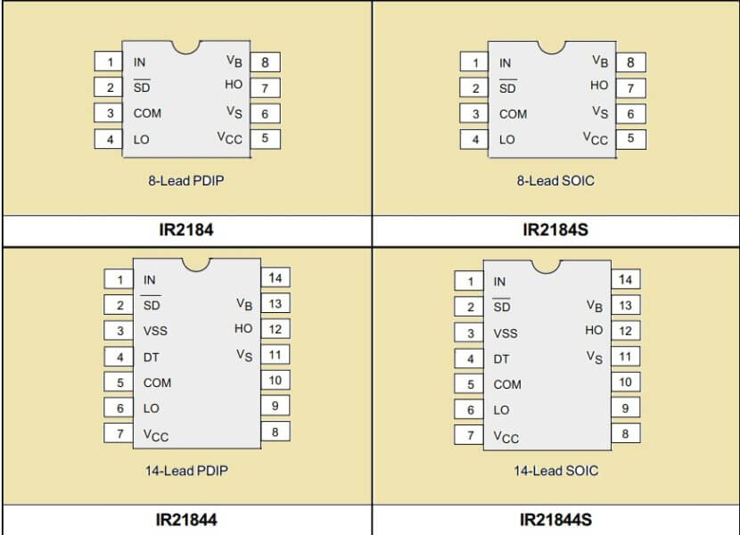
| Pin No. | Pin Name | Function Description |
|---|---|---|
| 1 | VCC | Logic supply voltage input (typically 10V to 20V) |
| 2 | IN | Logic-level input for switching both high-side and low-side |
| 3 | SD | Shut-down pin. When this is LOW, output is disabled |
| 4 | COM | Ground reference for low-side driver |
| 5 | LO | Output for low-side gate driver (connects to lower MOSFET gate) |
| 6 | VS | Source of high-side driver (connected to MOSFET source and load node) |
| 7 | HO | Output for high-side gate driver (connects to upper MOSFET gate) |
| 8 | VB | Bootstrap supply voltage (connected to bootstrap cap and diode) |
Absolute Maximum Ratings (from Datasheet)
| Parameter | Rating |
|---|---|
| VCC to COM | -0.3V to +25V |
| VB to COM | -0.3V to +625V |
| VS to COM | -5V to +600V (transient -10V for 50ns) |
| HO, LO Output Current | ±2A (source/sink) |
| Logic Input (IN, SD) | -0.3V to VCC + 0.3V |
| Power Dissipation | 1W max (depends on PCB layout) |
| Junction Temperature | -55°C to +150°C |
Recommended Operating Conditions
| Parameter | Typical Range |
|---|---|
| VCC | 10V to 20V |
| Logic input voltage | 0 to 5V |
| Bootstrap voltage (VB - VS) | 10V to 20V |
| Frequency | Up to 500 kHz |
| Dead-time (typical) | 500ns |
| Propagation Delay | ~540ns typical |
How the IC IR2184 Works
So this IC IR2184 is mainly working like a logic translator and MOSFET driver. We apply just one PWM signal at IN pin and this IC will smartly switch HO and LO outputs alternatively – never together. This is done by internal dead-time circuit which stops both transistors from turning on at the same time (which can burn the MOSFETs due to shoot-through current).

The HO output controls the high-side N-channel MOSFET gate and the LO output controls the low-side MOSFET. Bootstrap capacitor connected between VB and VS gives the required gate voltage to HO (because high-side gate needs to be above source level).
SD pin is a shutdown input. When this pin is LOW then IC disables both HO and LO. When SD is HIGH then IC runs normally. If we do not want to use SD function then we can just connect it to VCC.
How the IC IR21844 Works
So the next diagram below is showing a full half-bridge gate driver stage using IR21844, which is actually same like IR2184 but with internal shoot-through protection using dead-time pin (DT).
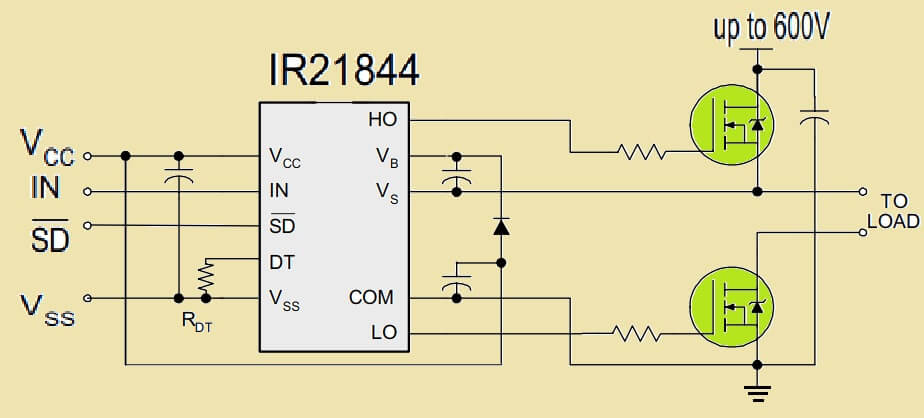
This driver IC is controlling two N-channel MOSFETs connected in half-bridge setup for switching high voltage DC (up to 600V) into some load, maybe a transformer, motor or whatever.
Pinout Details of IR21844 (Same like IR2184):
| Pin Name | Pin Type | What It Does (In Crude Words) |
|---|---|---|
| Vcc | Power Input | 12V supply input to IC (typically 10V to 20V) |
| IN | Logic Input | Main PWM signal input from microcontroller |
| SD | Logic Input | Shutdown control (active LOW). When LOW, both MOSFETs OFF |
| DT | Resistor Pin | This sets dead time (anti-shoot-through time) using resistor |
| Vss | GND Side | Ground for logic section (connect to COM) |
| COM | GND Side | Ground for output driver (same as Vss) |
| LO | Output | Goes to gate of low-side MOSFET |
| HO | Output | Goes to gate of high-side MOSFET |
| VB | Supply Pin | High-side driver positive supply (bootstrapped) |
| VS | Supply Pin | High-side driver return path (connected to source of top MOSFET) |
Component Breakdown and Values (Suggested):
| Part | Value / Note |
|---|---|
| R_DT | 22k to 33k typical (Sets dead-time ~0.5us to 1.5us) |
| Vcc | 12V (Can be from 10V to 20V max) |
| Bootstrap Cap | 0.47uF / 25V MLCC (from Vcc to VB) |
| Capacitor on Vcc pin | 1uF to 10uF / 25V (ceramic best) |
| Gate Resistors | 10Ω to 33Ω (optional, to slow gate rise) |
| High-side MOSFET | Any N-channel 600V 10A+ rated one |
| Low-side MOSFET | Same as above |
| High Voltage DC Bus | Up to 600V max |
| Load | Could be motor, transformer or anything |
Bootstrapping Section (Important to Note):
- The diode between Vcc and VB cap is internal in IR21844 so we do not need to add external diode.
- Cap from VB to VS is the bootstrap capacitor (marked here) — this stores the charge needed to turn ON the high-side MOSFET.
- Whenever the low-side MOSFET conducts, VS is pulled to GND, so the boot cap charges through internal diode from Vcc.
So this charging happens automatically, no extra control needed.
Important Notes:
- Vcc and COM must be tightly bypassed with 1uF to 10uF cap, or else IC will behave erratically.
- Never forget gate resistors (10Ω to 33Ω), else the MOSFETs might heat due to fast switching noise.
- R_DT (dead time) ensures both MOSFETs are not ON at the same time, which would cause short circuit (shoot-through).
Working Flow:
- IN pin gets PWM signal from microcontroller or any oscillator IC like IC 555.
- IR21844 decodes this to drive HO and LO pins alternately.
- LO pin drives bottom MOSFET which connects load to GND.
- HO pin drives top MOSFET which connects load to high voltage DC.
- Bootstrap cap keeps high-side floating driver alive with VB - VS = Vcc.
- Dead-time pin makes sure there’s no overlap while switching.
Bootstrap Circuit Basics
To make HO output work properly, we must use a bootstrap diode and bootstrap capacitor. The diode charges the capacitor when LO is ON and this stored voltage is used for turning ON the high-side MOSFET.
Typical Bootstrap Circuit:
- Diode: Fast recovery type like UF4007 or 1N4148.
- Capacitor: Between 0.1uF and 1uF, non-polar ceramic or film.
Calculating Bootstrap Capacitor
Here is one basic formula for calculating the bootstrap capacitor value:
Cb = Qg / ΔV
Where:
- Cb = Bootstrap capacitor value.
- Qg = Total gate charge of high-side MOSFET (from MOSFET datasheet).
- ΔV = Allowed voltage drop across capacitor (normally 1V to 2V).
Example:
Suppose we are using IRF540N which has Qg = 71nC
Let ΔV = 1V
Then:
Cb = 71nC / 1V = 71nF, so we choose standard 100nF or 0.1uF
Better to use 0.22uF or 0.47uF for extra safety.
Applications
- Full-Bridge or Half-Bridge Inverter.
- DC-AC Converters.
- BLDC Motor Drivers.
- Induction Heater.
- High Voltage Buck/Boost Converters.
- Sine wave Inverter.
- Class D Amplifier Gate Driver.
Advantages of IR2184(4)
- High side and low side both are driven properly.
- Needs only one logic signal for operation.
- Has inbuilt dead-time so shoot-through cannot happen.
- Works up to 600V load easily.
- Fast switching up to 500 kHz.
- Only one bootstrap cap and diode required.
- Very compact 8-pin design.
- SD pin gives safety control.
Why We Cannot Drive Power MOSFETs Directly?
Now first let us ask this – can we drive a big power MOSFET like IRFP2907 or IRF3205 directly from Arduino or microcontroller?
Answer is no, because microcontroller can give only small current like 20mA or 30mA. But these big MOSFETs need instant gate current of 1A to 3A or even more for turning ON/OFF fast. If we give slow current, MOSFET will heat up, switch slow and may even burn.
Also, high-side MOSFET is not easy to drive. Its source pin is jumping up and down with output voltage and gate needs to be always 10V higher than source. That is why, we cannot drive it using simple logic.
So what we need?
We need one strong IC that can give big current quickly and also handle this jumping voltage condition. That is exactly where IR2184 or IR21844 comes in.
Main Job of IR2184: Act Like Gate-Current Booster for MOSFETs
We can say like this – IR2184 is acting like one current amplifier for microcontroller. It takes small signal from Arduino and gives strong drive to both MOSFETs – high-side and low-side.
When IN pin is HIGH:
- Low-side MOSFET is OFF.
- Bootstrap capacitor already charged.
- HO pin goes HIGH → Turns ON the high-side MOSFET.
When IN pin is LOW:
- High-side MOSFET is OFF.
- Bootstrap cap gets charged again.
- LO pin goes HIGH → Turns ON low-side MOSFET.
And the best part? It keeps some delay (dead-time) between these two states, so both MOSFETs never turn ON at same time. This prevents shoot-through current which can destroy the circuit.
How It Helps in Building High Power Inverter?
Let us say we want to make 500W, 1000W, or even 3000W sine wave inverter. In that case, we need to switch big MOSFETs or IGBTs with high current rating.
For example:
- IRF3205 = 110A, 55V
- STGW30NC60VD = 30A, 600V IGBT
Such devices have gate charge over 100nC to 200nC, and they need fast current pulses like 2A to 3A.
If we try to drive them directly then they will switch slow, get hot, create noise and waste power.
But with IR2184:
- We can feed small PWM signal from Arduino.
- It will give strong drive (2A peak) to big MOSFETs.
- It will isolate low-voltage logic from high-voltage side.
- It will generate correct timing using dead-time.
- It will help manage both sides of inverter H-bridge properly.
So we can use 2nos IR2184 ICs for full bridge (4 MOSFETs) and build full sine wave inverter easily.
Example Setup for 1kW Inverter:
- Microcontroller: Arduino or SG3525 or TL494.
- Gate Driver: 2 x IR2184.
- MOSFETs: 4 x IRFP260 (or 4 x IRF3205 for low voltage).
- Output Transformer: 12V to 220V.
- Load: AC fan, light, pump etc.
Just apply PWM to both IR2184s with 180° phase shift and thats it – full H-bridge inverter will run smooth, cool and powerful.
So in one sentence – IR2184 helps us to handle very big and high current MOSFETs by giving strong, safe, isolated gate signals. It allows us to control dangerous 400V or 600V power with simple 5V logic PWMs, without burning anything. That is why, it is like the heart of every modern inverter, motor driver and high power switching system.
Conclusion
So friends, finally we can say that this IR2184 or IR21844 is very smart half bridge gate driver IC for switching big MOSFETs with safe and stable method. We can use it in many circuits where we want to control high power through small PWM signal. Just make sure to add bootstrap capacitor and fast diode and do not forget to give proper VCC to the IC (like 12V). Then it will work solid and reliable for all inverter or driver applications.


Need Help? Please Leave a Comment! We value your input—Kindly keep it relevant to the above topic!