

In this post we discuss 4 easy to build, compact simple transformerless power supply circuits. All the circuits presented here are built using capacitive reactance theory for stepping down the input AC mains voltage. All the designs presented here work independently without any transformer, or no transformer.
The Transformerless Power Supply Concept
As the name defines, a transformerless power supply circuit provides a low DC from the mains high voltage AC, without using any form of transformer or inductor.
It works by using a high voltage capacitor to drop the mains AC current to the required lower level which may be suitable for the connected electronic circuit or load.
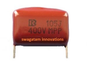
The voltage specification of this capacitor is selected such that it's RMS peak voltage rating is much higher than the peak of the AC mains voltage in order to ensure safe functioning of the capacitor. An example capacitor which is normally used transformerless power supply circuits is shown below:

This capacitor is applied in series with one of the mains inputs, preferably the phase line of the AC.
When the mains AC enters this capacitor, depending on the value of the capacitor, the reactance of the capacitor comes into action and restricts the mains AC current from exceeding the given level, as specified by the value of the capacitor.
However, although the current is restricted the voltage isn't, therefore if you measure the rectified output of a transformerless power supply you will find the voltage to be equal to the peak value of the mains AC, that's around 310V, and this could be alarming for any new hobbyist.
But since the current may be sufficiently dropped level by the capacitor, this high peak voltage could be easily tackled and stabilized by using a zener diode at the output of the bridge rectifier.
The zener diode wattage must be appropriately selected according to the permissible current level from the capacitor.
WARNING: BE EXTREMELY CAREFUL WHILE TESTING THE CIRCUITS EXPLAINED BELOW SINCE THEY ARE NOT ISOLATED FROM AC MAINS, AND CAN PRODUCE LETHAL ELECTRIC SHOCK IF TOUCHED DIRECTLY IN AN UNCOVERED AND POWERED CONDITION. MAKE SURE TO PROPERLY INSULATE ALL THE POINTED OR EXPOSED CONNECTIONS OF THE WIRING. WE STRICTLY CAUTION YOU THAT YOU BUILD THESE CIRCUITS ONLY IF YOU ARE AWARE OF THE DANGERS OF MAINS AC AND KNOW HOW TO MAINTAIN EXTREME SAFETY AGAINST IT.
NOTE: The transformerless power supply circuits explained below are specifically intended to be used as cheap and compact power supply alternatives for powering small circuits. For maximum safety the user must ensure that the whole assembly is enclosed inside a well insulated box such as a plastic box. These circuits are NOT intended to be used as AC to DC adapters for powering external gadgets.
Advantages of using a Transformerless Power Supply Circuit
The idea is cheap yet very effective for applications that require low power for their operations.
Using a transformer in DC power supplies is probably quite common and we have heard a lot regarding it.
However one downside of using a transformer is that you cannot make the unit compact.
Even if the current requirement for your circuit application is low, you have to include a heavy and bulky transformer making things really cumbersome and messy.
The transformerless power supply circuit described here, very efficiently replaces a usual transformer for applications which require current below 100 mA.
Here a high voltage metalized capacitor is used at the input for the required stepping down of the mains power and the preceding circuit is nothing but just simple bridge configurations for converting the stepped down AC voltage to DC.
The circuit shown in the diagram above is a classic design may be used as a 12 volts DC power supply source for most electronic circuits.
However having discussed the advantages of the above design, it will be worth focusing on a few serious drawback this concept may include.
Disadvantages of a Transformerless Power Supply Circuit
First, the circuit is unable to produce high current outputs, but that won’t make an issue for most of the applications.
Another drawback that certainly needs some consideration is that the concept does not isolate the circuit from dangerous AC mains potentials.
This drawback can have serious impacts for designs which have terminated outputs or metal cabinets, but won’t matter for units which have everything covered up in a non-conducting housing.
Therefore, new hobbyists must work with this circuit very carefully to avoid any electrical casualty. The last but not the least, the above circuit allows voltage surges to enter through it, which may cause serious damage to the powered circuit and to the supply circuitry itself.
However in the proposed simple transformerless power supply circuit design this drawback has been reasonably tackled by introducing different types of stabilizing stages after the bridge rectifier.
This capacitor grounds instantaneous high voltage surges, thus efficiently safeguarding the associated electronics with it.
How the Circuit Works
The working of this transformless power supply can be understood with the following points:
- When mains AC mains input is switched ON, capacitor C1 blocks the entry of the mains current and restricts it to a lower level as determined by the reactance value of C1. Here it may be roughly assumed to be around 50mA.
- However, the voltage is not restricted, and therefore the full 220V or whatever may be at the input is allowed to reach the subsequent bridge rectifier stage.
- The bridge rectifier rectifies this 220V C to a higher 310V DC, due to the RMS to peak conversion of the AC waveform.
- This 310V DC is instantly reduced to a low level DC by the next zener diode stage, which shunts it to the zener value. If a 12V zener is used, this will become 12V and so on.
- C2 finally filters the 12V DC with ripples, into a relatively clean 12V DC.
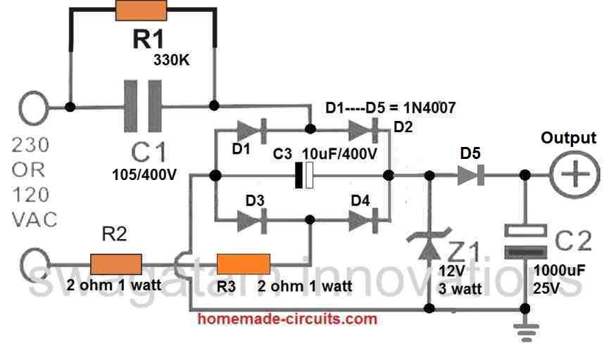
1) Basic Transformerless Design

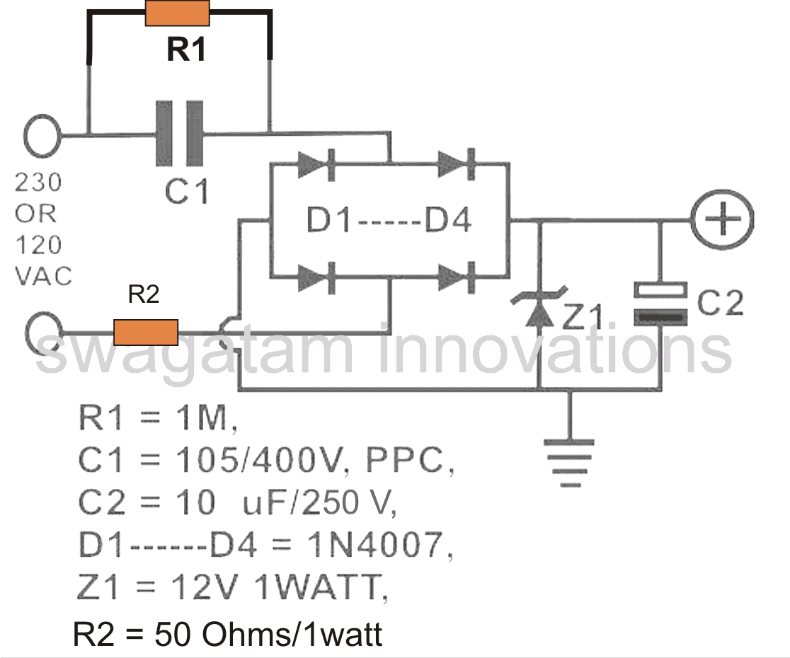
Let's try to understand the function of each of the parts used in the above circuit, in greater details:
- The Capacitor C1 becomes the most important part of the circuit since it is the one that reduces the high current from the 220 V or 120 V mains to the desired lower level, to suit the output DC load. As a rule of thumb every single single microFarad from this capacitor will provide around 50 mA current to the output load. This means, a 2uF will provide 100 mA and so on. If you wish to learn the calculations more precisely you can refer to this article.
- The resistor R1 is used for providing a discharge path for the high voltage capacitor C1 whenever the circuit is unplugged from the mains input. Because, C1 has the ability to store the 220 V mains potential in it when it is detached from the mains, and could risk a high voltage shock to whoever touches the plug pins. R1 quickly discharges the C1 preventing any such mishap.
- Diodes D1---D4 work like a bridge rectifier for converting the low current AC from the C1 capacitor into a low current DC. The capacitor C1 restricts the current to 50 mA but does not restrict the voltage. This implies that the DC at the the output of the bridge rectifier is the peak value of the 220 V AC. This can be calculated as: 220 x 1.41 = 310 V DC approximately. So we have 310 V, 50 mA at the output of the bridge.
- However, the 310V DC may be too high for any low voltage device except a relay. Therefore, an appropriately rated zener diode is used for shunting the 310V Dc into the desired lower value, such as 12 V, 5 V, 24 V etc, depending on the load specs.
- Resistor R2 is used as a current limiting resistor. You may feel, when C1 is already there for limiting the current why do we need the R2. It is because, during the instantaneous power switch ON periods, meaning when the input AC is first applied to the circuit, the capacitor C1 simply acts like a short circuit for a few milliseconds. These few initial milliseconds of the switch ON period, allows the full AC 220 V high current to enter the circuit, which may be enough to destroy the vulnerable DC load at the output. In order to prevent this we introduce R2. However, the better option could be to use an NTC in place of R2.
- The C2 is the filter capacitor, which smoothens the 100 Hz ripples from the rectified bridge to a cleaner DC. Although a high voltage 10uF 250V capacitor is shown in the diagram, you can simply replace it with a 220uF/50V due to the presence of the zener diode.
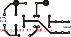
PCB Layout for the above explained simple transformerless power supply is shown in the following image. Please note that I have included a space for an MOV also in the PCB, at the mains input side.
Improving the Design
The above transformerless design looks simple, but it has some unavoidable downsides. The resistor R2 is mandatory in the circuit, otherwise the zener diode may burn instantly. However, adding the resistor R2 causes a significant drop in the output current, and there's also some serious dissipation through the resistor R2, making the circuit somewhat inefficient.
The idea to make sure that R2 is as low as possible, yet the entire circuit remains completely safe from all possible electrical hazards.
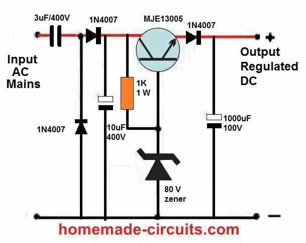
For this, we reinforce the zener diode with a high voltage transistor wired in the crowbar format, as shown in the following diagram:

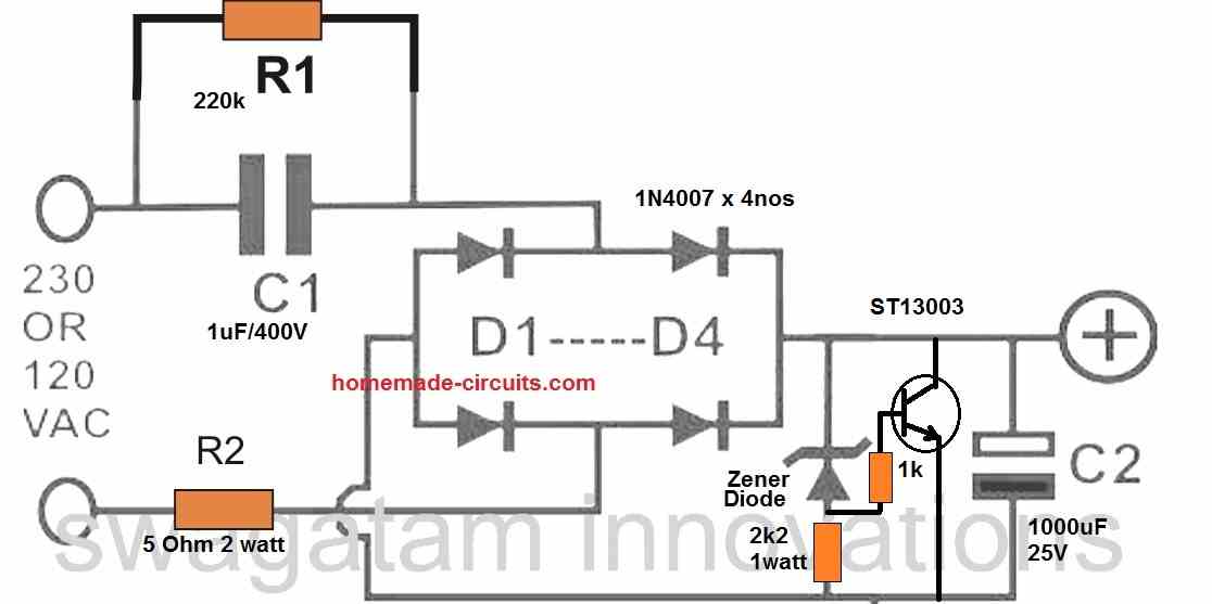
The design looks entirely fail-proof, yet provides a perfectly stabilized output. The power transistor ST13003 is used like a shunting device, which grounds the entire power from the capacitor C1 as soon as the output DC from the bridge tries to reach above the zener diode level.
In this situation, the transistor conducts and shorts circuits the DC causing the voltage to drop.
When the voltage drops, the zener stops conducting switching OFF the transistor, and the cycle keeps repeating at a fast rate, enabling a stabilized DC output voltage that is almost equal to the zener voltage value.
If you do not wish to include the power transistor, you can also modify first design in the following manner:

Here we have introduced 3 improvements in the circuit. We have used two current limiting resistor through R2 and R3, so that the surge current is shared across both the resistors uniformly. We have introduced C3 which helps to ground and absorb the initial switch ON surge current to a great extent causing less stress on the zener diode.
We have also increased the rating of the zener diode to 3 watts so that it does not burn under any circumstances.
You can further improve the above transformerless power supply design by replacing R2 and R3 with a single 5 ohm NTC thermistor.
The above design can be improved even further by doing the following modifications:

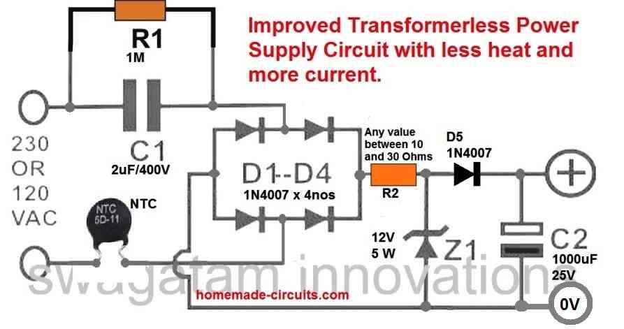
You can see we have entirely removed the capacitor across the bridge rectifier which makes the load on the zener diode 50% less, creating 50% less heat.
The filter capacitor can be seen after the diode D5 which means the capacitor voltage is much reduced to only 25V and the filtration is increased to a very high level due to the high value of 1000 uF.
Another Simple Transformerless Power Supply for long LED Strings

The above transformerless power supply circuit uses an MJE13005 transistor as an emitter follower regulator with a base zener diode to regulate the output voltage. The input side includes a 3uF/400V capacitor to limit the maximum output current to around 150 mA, and two diodes (horizontal and vertical) are used for rectification, converting AC voltage to pulsating DC voltage.
Example Circuit for LED Decoration Light Application
The following transformerless or capacitive power supply circuit could be used as an LED lamp circuit for illuminating minor LED circuits, such as small LED bulbs or LED string lights.
Remember, since the circuit is not isolated from AC mains the whole wiring can carry lethal AC mains voltages. Please build it only if you exactly know how to correctly insulate the circuit using plastic covers and plastic sleeves. Do it at your own risk.
The idea was requested by Mr. Jayesh:
Requirement Specifications
The string is made up of about 65 to 68 LED of 3 Volt in series approximately at a distance of let us say 2 feet ,,, such 6 strings are roped together to make one string so the bulb placement comes out to be at 4 inches in final rope . so over all 390 - 408 LED bulbs in final rope.
So please suggest me best possible driver circuit to operate
1) one string of 65-68 string.
or
2) complete rope of 6 strings together.
we have another rope of 3 strings.The string is made up of about 65 to 68 LED of 3 Volt in series approximately at a distance of let us say 2 feet , such 3 strings are roped together to make one string so the bulb placement comes out to be at 4 inches in final rope . so over all 195 - 204 LED bulbs in final rope.
So please suggest me best possible driver circuit to operate
1) one string of 65-68 string.
or
2) complete rope of 3 strings together.
Please suggest the best robust circuit with surge protector and advice any additional things to be connected to protect the circuits.
and please see that circuit diagrams are with values required for the same as we are not at all technical person in this field.
Circuit Design
The driver circuit shown below is suitable for driving any LED bulb string having less than 100 LEDs (for 220V input), each LED rated at 20mA, 3.3V 5mm LEDs:

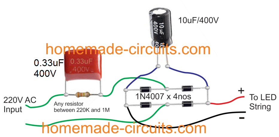
Here the input capacitor 0.33uF/400V decides the amount of current supplied to the LED string. In this example it will be around 17mA which is just about right for the selected LED string.
If a single driver is used for more number of similar 60/70 LED strings in parallel, then simply the mentioned capacitor value could be proportionately increased for maintaining optimal illumination on the LEDs.
Therefore for 2 strings in parallel, the required value would be 0.68uF/400V, for 3 strings you could replace it with a 1uF/400V. Similarly for 4 strings this would need to be upgraded to 1.33uF/400V, and so on.
Important: Although I have not shown a limiting resistor in the design, it would be a good idea to include a 33 Ohm 2 watt resistor in series with each LED string for added safety. This could be inserted anywhere in series with the individual strings.
WARNING: ALL THE CIRCUITS MENTIONED IN THIS ARTICLE ARE NOT ISOLATED FROM MAINS AC, THEREFORE ALL THE SECTIONS IN THE CIRCUIT ARE EXTREMELY DANGEROUS TO TOUCH WHEN CONNECTED TO MAINS AC........
2) Upgrading to Voltage Stabilized Transformerless Power Supply
Now let's see how an ordinary capacitive power supply may be transformed into a surge free voltage stabilized or variable voltage transformerless power supply applicable for almost all standard electronic loads and circuits. The idea was requested by Mr. Chandan Maity.
Technical Specifications
If you remember, I communicated you sometime before with comments at your blog.
The Transformerless circuits are really good and I tested couple of those and running 20W, 30W LED.Now, I am trying to add some controller, FAN and LED all together , hence, I need a dual supply.
The rough specification is:
Current rating 300 mAP1= 3.3-5V 300mA ( for controller etc)P2= 12-40V (or higher range), 300mA (for LED)
I thought to use your 2nd circuit as mentionedhttps://www.homemade-circuits.com/2012/08/high-current-transformerless-power.html
But, I am not able to freeze the way how to get 3.3V without using extra capacitor. 1. Can, a second circuit may be placed from the output of first one? 2. Or, a second TRIAC, bridge to be placed in parallel with first one, after capacitor to get 3.3-5V
I shall be glad if you kindly help.
Thanks,
The Design
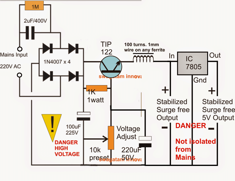
The function of the various components used across the various stages of the above shown voltage controlled circuit may be understood from the following points:
The mains voltage is rectified by the four 1N4007 diodes and filtered by the 10uF/400V capacitor.
The output across the 10uF/400V now reaches around 310V which is the peak rectified voltage achieved from the mains.
The voltage divider network configured at the base of the TIP122 makes sure that this voltage is reduced to the expected level or as required across the power supply output.
You can also use MJE13005 in place of TIP122 for better safety.
If a 12V is required the 10K pot may be set to achieve this across the emitter/ground of the TIP122.
The 220uF/50V capacitor ensures that during switch ON the base is rendered a momentary zero voltage in order to keep it switched OFF and safe from the initial surge in-rush.
The inductor further ensures that during the switch ON period the coil offers a high resistance and stops any inrush current to get inside the circuit, preventing a possible damage to the circuit.
For achieving a 5V or any other attached stepped down voltage, a voltage regulator such as the shown 7805 IC may be used for achieving the same.
Circuit Diagram

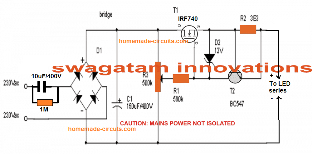
Using MOSFET Control
The above circuit using emitter follower can be further enhanced by applying a MOSFET source follower power supply, along with a supplemental current control stage using BC547 transistor.
The complete circuit diagram can be seen below:

Video Proof of Surge Protection

3) Zero Crossing Transformerless Power Supply Circuit
The third interesting explains the importance of a zero crossing detection in capacitive transformerless power supplies in order to make it completely safe from the mains switch ON inrush surge currents. The idea was proposed by Mr. Francis.
Technical Specifications
I have been reading about the transformer less power supply articles on your site with great interest and if I am understanding correctly the main problem is the possible in-rush current in the circuit upon switching-on, and this is caused because switching-on does not always occur when the cycle is at zero volts (zero crossing).
I am a novice in electronics and my knowledge and practical experience are very limited, but if the problem can be solved if zero crossing is implemented why not use a zero crossing component to control it such as an Optotriac with zero crossing.
The input side of the Optotriac is low power therefore a low power resistor can be used to lower the mains voltage for Optotiac operation. Therefore no capacitor is used at the Optotriac’s input. The capacitor is connected on the output side which will be switched on by the TRIAC which turns on at zero crossing.
If this is applicable it will also solve high current requirement problems, since the Optotriac in turn can operate another higher current and/or voltage TRIAC without any difficulty. The DC circuit connected to the capacitor should no longer have the in-rush current problem.
It would be nice to know your practical opinion and thank you for reading my mail.
Regards,
Francis
The Design
As rightly pointed out in the above suggestion, an AC input without a zero crossing control can be a major cause of a surge current inrush in capacitive transformerless power supplies.

Today with the advent of sophisticated triac driver opto-isolators, switching an AC mains with zero crossing control is no longer a complex affair, and can be simply implemented using these units.
About MOCxxxx Opto-couplers
The MOC series triac drivers come in the form of optocouplers and are specialists in this regard and can be used with any triac for controlling AC mains through a zero crossing detection and control.
The MOC series triac drivers include MOC3041, MOC3042, MOC3043 etc all these are almost identical with their performance characteristics with only minor differences with their voltage spces, and any of these can be used for the proposed surge control application in capacitive power supplies.
The zero crossing detection and execution are all internally processed in these opto driver units and one has to only configure the power triac with it for witnessing the intended zero crossing controlled firing of the integrated triac circuit.
Before investigating the surge free triac transformerless power supply circuit using a zero crossing control concept let's first understand briefly regarding what's a zero crossing and its involved features.
What is Zero Crossing in AC Mains
We know that an AC mains potential is composed of voltage cycles which rise and fall with changing polarity from zero to maximum and vice versa across the given scale.
For example in our 220V mains AC, the voltage switches from 0 to +310V peak) and back to zero, then forwarding downwards from 0 to -310V, and back to zero, this goes on continuously 50 times per second constituting a 50 Hz AC cycle.
When the mains voltage is near its instantaneous peak of the cycle, that is near 220V (for a 220V) mains input, it's in the strongest zone in terms of voltage and current, and if a capacitive power supply happens to be switched ON during this instant, the entire 220V can be expected to break through the power supply and the associated vulnerable DC load.
The result could be what we normally witness in such power supply units.... that is instant burning of the connected load.
The above consequence may be commonly seen only in capacitive transformerless power supplies because, capacitors have the characteristics of behaving like a short for a fraction of a second when subjected to a supply voltage, after which it gets charged and adjusts to its correct specified output level
Coming back to the mains zero crossing issue, in a converse situation while the mains is nearing or crossing the zero line of its phase cycle, it can be considered to be in its weakest zone in terms of current and voltage, and any gadget switched ON at this instant can be expected to be entirely safe and free from a surge inrush.
Therefore if a capacitive power supply is switched ON in situations when the AC input is passing through its phase zero, we can expect the output from the power supply to be safe and void of a surge current.
How it Works
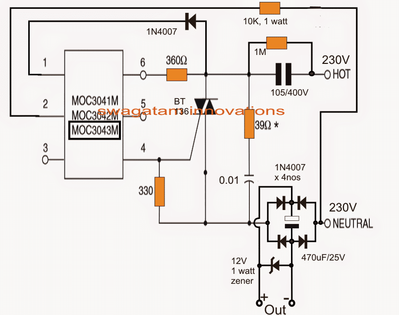
The circuit shown above utilizes a triac optoisolator driver MOC3041, and is configured in such a way that whenever power is switched ON, it fires and initiates the connected triac only during the first zero crossing of the AC phase, and then keeps the AC switched ON normally for rest of the period until power is switched OFF and switched ON again.
Referring to the figure we can see how the tiny 6-pin MOC 3041 IC is connected with a triac for executing the procedures.
The input to the triac is applied through a high voltage, current limiting capacitor 105/400V, the load can be seen attached to the other end of the supply via a bridge rectifier configuration for achieving a pure DC to the intended load which could an LED.
How Surge Current is Controlled
Whenever power is switched ON, initially the triac stays switched OFF (due to an absence of the gate drive) and so does the load connected to the bridge network.
A feed voltage derived from the output of the 105/400V capacitor reaches the internal IR LED through the pin1/2 of the opto IC.
This input is monitored and processed internally with reference to the LED IR light response.... and as soon the fed AC cycle is detected reaching the zero crossing point, an internal switch instantly toggles and fires the triac and keeps the system switched ON for the rest of the period until the unit is switched OFF and ON yet again.
With the above set up, whenever power is switched ON, the MOC opto isolator triac makes sure that the triac is initiated only during that period when the AC mains is crossing the zero line of its phase, which in turn keeps the load perfectly safe and free from the dangerous surge in rush.
Improving the above Design
A comprehensive capacitive power supply circuit having a zero crossing detector, a surge suppressor and voltage regulator is discussed here, the idea was was submitted by Mr. Chamy
Designing an Improved Capacitive Power Supply Circuit with Zero Crossing Detection
Hello Swagatam.
This is my zero crossing, surge protected capacitive power supply design with voltage stabilizer,i will try to list all of my doubts.
(I know this will be expensive for the capacitors,but this is only for testing purposes)

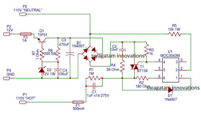
1-I'm not sure if the BT136 haves to be changed for a BTA06 for accommodating more current.
2-The Q1 (TIP31C) can handle only 100V Max. Maybe it should be changed for a 200V 2-3A transistor?,like the 2SC4381.
3-R6 (200R 5W),I know this resistor is pretty small and its my
fault,i actually wanted to put a 1k resistor.But with an 200R 5W
resistor it would work?
4-Some resistors have been changed following your recommendations to make it 110V capable.Maybe the 10K one needs to be smaller?
If you know how to make it work correctly,i will be very happy to correct it.If it works i can make a PCB for it and you could publish it in your page (For free of course).
Thank you for taking the time and viewing my full of faults circuit.
Have a nice day.
Chamy
Assessing the The Design
Hello Chamy,
your circuit looks OK to me. Here are the answers to your questions:
1) yes BT136 should be replaced with a higher rated triac.
2) TIP31 can be replaced with a 200V Darlington transistor such as BU806 etc otherwise it might not work properly.
3) when a Darlington is used the base resistor could be high in value, may be a 1K/2 watt resistor would be quite OK.
However the design by itself looks like an overkill, a much simpler version can be seen below https://www.homemade-circuits.com/2016/07/scr-shunt-for-protecting-capacitive-led.html
Regards
Swagatam
Reference:
4) Switching Transformerless Power Supply using IC 555
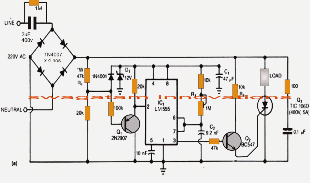
This 4rth simple yet smart solution is implemented here using IC 555 in its monostable mode to control in rush surge in a transfomerless power supply via a zero crossing switching circuit concept, wherein the input power from the mains is allowed to enter the circuit only during the zero crossings of the AC signal, thereby eliminating the possibility of surge inrushes. The idea was suggested by one of the avid readers of this blog.
Technical Specifications
Would a zero cross transformerless circuit work to prevent the initial inrush current by not allowing turn on until the 0 point in the 60/50 hertz cycle?
Many solid state relays which are cheap, less then INR 10.00 and have this ability built in them.
Also I would like to drive 20watt leds with this design but am unsure how much current or how hot capacitors will get I suppose it depends on how the leds are wired series or parallel, but lets say the capacitor is sized for 5 amps or 125uf will the capacitor heat up and blow???
How does one read capacitor specs to determine how much energy they can dissipate.
The above request prompted me to look for a related design incorporating a IC 555 based zero crossing switching concept, and came across the following excellent transformerless power supply circuit which could be used for convincingly eliminating all possible chances of surge inrush.
What's a Zero Crossing Switching:
It's important to learn this concept first before investigating the proposed surge free transformerless circuit.
We all know how a sine wave of an AC mains signal looks like. We know that this sine signal starts from a zero potential mark, and exponentially or gradually rises to the peak voltage (220 or 120) point, and from there exponentially reverts to the zero potential mark.
After this positive cycle, the waveform dips and repeats the above cycle but in the negative direction until it comes back yet again to the zero mark.
The above operation happens about 50 to 60 times per second depending upon the mains utility specs.
Since this waveform is what enters the circuit, any point in the waveform other than the zero, presents a potential danger of a switch ON surge due to the involved high current in the waveform.
However the above situation can be avoided if the load confronts the switch ON during the zero crossing, after which the rise being exponential doesn't pose any threat to the load.
This is exactly what we have tried to implement in the proposed circuit.
Circuit Operation
Referring to the circuit diagram below, the 4 1N4007 diodes form standard bridge rectifiers configuration, the cathode junction produces a 100Hz ripple across the line.
The above 100Hz frequency is dropped using a potential divider (47k/20K) and applied to the positive rail of the IC555. Across this line the potential is appropriately regulated and filtered using D1 and C1.
The above potential is also applied to the base Q1 via the 100k resistor.
The IC 555 is configured as an monostable MV which means its output will go high every time its pin#2 is grounded.
For the periods during which the AC mains is above (+)0.6V, Q1 stays switched OFF, but as soon as the AC waveform touches the zero mark, that is reaches below the (+)0.6 V, Q1 switches ON grounding pin#2 of the IC and rendering a positive output of the IC pin#3.
The output of the IC switches ON the SCR and the load and keeps it switched ON until the MMV timing elapses, to begin a new cycle.
The ON time of the monostable can be set by varying the 1M preset.
Greater ON time ensures more current to the load, making it brighter if it's an LED, and vice versa.
The switch ON conditions of this IC 555 based transformerless power supply circuit is thus restricted only when the AC is near zero, which in turn ensures no surge voltage each time the load or the circuit is switched ON.
Circuit Diagram

For LED Driver Application
If you are looking for a transformerless power supply for LED driver application at commercial level, then probably you can try the concepts explained here.
Transformerless 220 V to 50 V Converter Circuit
The bridge-rectifier BR1 receives the AC voltage from PL1 and produces a fullwave output of about 300 volts DC. A sequence of 5 volt pulses are produced by the network R1, R2, D1, D3, and D4 and serve two crucial purposes:

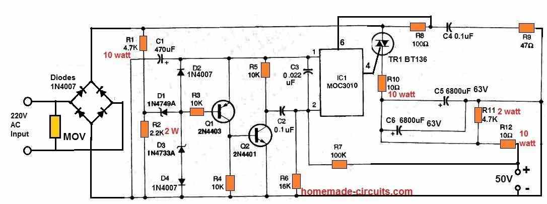
Firstly, using D2 and C1, the pulses are employed as a 5-volt power supply for the monostable circuit and pulse shaping.
Secondly, the pulses activate the monostable circuit formed of C2 and R6, the pulse-shaping circuit consisting of Q1, Q2, and R3-R5, and the optoisolator 1C1 and power-triac TR1.
The peak output voltage is determined by resistor R2, which also controls the highest pulse width.
If the feedback network is removed the output peak voltage would be about 90 volts. The feedback configuration made up of R6, R7, and C3 reverse biases the optoisolator whenever the output voltage increases beyond 50 volts in order to get the desired 50 volt output.
The unregulated voltage then drops to zero volts, forcing TR1 to switch off. Thus, the RC feedback circuitry effectively modifies the conduction state of 1C1 to control the output voltage.
The optoisolator's current is limited by resistor R8, and C4 and R9 guarantees its constant and stable functioning.
Additionally, R10 controls the surge current that passes across TR1 whenever the power is first switched on. A low-pass filter stage with the components R10, C5, and C6 reduces ripple current.
C5 and C6 are discharged by the resistor R11 whenever the power source is switched off.
New Entry: Cheap, Surge-Free Transformerless Power Supply (Recommended)
Recently, while exploring a cheaper version of a zero crossing based surge free transformerless power circuit I happened to design the following circuit, which looks very promising.
The following figure shows the full circuit diagram. I have not yet tested it but the working looks very obvious.

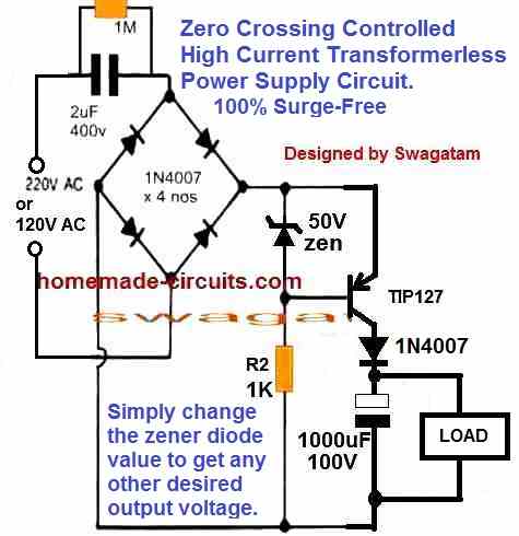
The working of the circuit is very interesting.
The input 2 uF capacitor drops the AC input current to 200 ma and feeds the 220 V to the bridge rectifier. The bridge rectifier rectifies the low current 220 V AC into a 310 V DC to the transistor/zener zero crossing controller circuit.
Now, as long as the output DC from the bridge is above the 50 V zener diode value, it keeps the transistor reverse biased and prevents it from conducting.
This means that, any form high voltage input surge is completely eliminated during any period of the AC cycle waveform.
However, each time the AC waveform reaches below the 50 V zener value, it causes the zener diode to shut off and allow the transistor to become forward biased through the 1 K resistor.
When this happens, the transistor conducts instantly and delivers the 50 V DC to the 1000 uF capacitor so that the voltage is stored inside the capacitor.
This stored voltage is subsequently fed to the load for a safe and a well regulated operation of the load.
The transistor and the zener network makes sure that the load gets the required operating voltage whenever the AC input voltage for this circuit is below 50 V.
This ensures that the load is never subjected to a switching high voltage or high current surge, and can operate safely without any relevant concerns.
One question though: is the shown transistor suitable for this circuit, since it is just 100 V rated? If you think otherwise you can simply replace it with a MJE5852 400 V transistor.