In this post I have explained how to build a battery deep discharge protection circuit which can be used for protecting any type of battery from over discharge through a connected load.
Normally, we are mostly worried about battery getting over charged, and forget about a situation where the battery can get over discharged by the load. Although, overcharging a battery may be detrimental to a battery health and appropriate measures must be incorporated, an over discharge or a deep discharge can be also equally dangerous for a battery's health.
In the following paragraphs I will elucidate a very simple design for shutting off the battery to the load, as soon as the battery voltage has reached the critical deep discharge state.
The circuit is fully solid-state and uses only transistors for the switching, thus eliminating the need of bulky relays.
Circuit Specifications
The idea was actually requested by one of the dedicated readers of this blog, Mr. Saurav, as I have explained below:
Looking for some ideas/help/suggestions. I have installed a 2.2 kw off grid solar system, using loom solar panels, excide battery and excide solar inverter. The inverter has this pre-setup priority, first solar, then grid, last battery. I have disconnected the mains supply to the inverter, so for me it is solar then battery. To this overall setup, I have added an ACCL with grid as secondary.
So in the evening, whenever there is no solar and the battery is out of charge, it falls back to grid power.
This setup has one problem. ACCL switches to mains power at night, when the battery is completely drained out or deeply discharged and that's what I don't want.
I want to turn off the battery power, when the battery has 20% remaining power or the battery is at a certain voltage. That way battery life can be better.
Is this something doable? Do we have something readily available for this? Or do we need to build something for this?
The Design
The circuit design for the proposed battery deep discharge protection circuit can be witnessed in the following diagram:
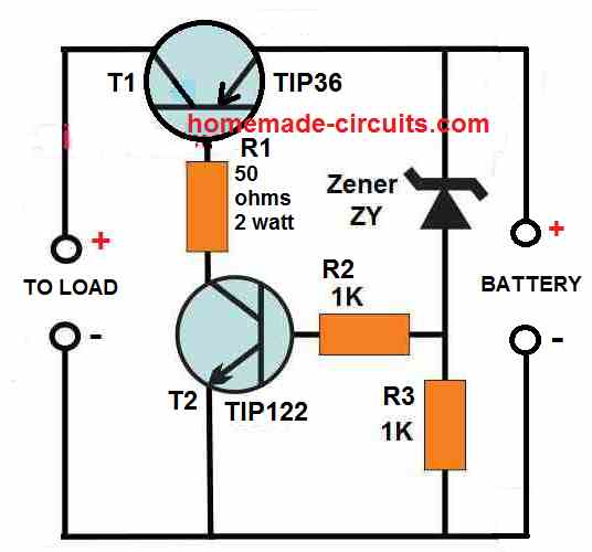
As can be seen, the circuit has a very components, and its working can be understood through the following points:
There are a couple of power transistors coupled with each other where, the base of the TIP36 transistor forms the collector load of the TIP122 transistors.
The base of TIP122 is biased through a resistor/zener diode network, where the zener diode ZY determines the cut off voltage for the TIP122.
The zener diode voltage is selected such that it matches the critical low voltage value of the battery, or any value at which the draining of the battery by the load is required to be stopped.
As long as the battery voltage stays above the zener voltage, or the voltage at which the cut-off needs to happen, the zener diode keeps conducting which in turn keeps the TIP122 in the conducting mode.
With TIP122 conducting the TIP36 gets the required base current, and it also conducts and allows the battery current to pass to the load.
However, the moment the battery voltages reaches or drops below the zener voltage which is also the deep discharge voltage level, causes the zener diode to stop conducting.
When the zener diode stops conducting, the TIP122 base voltage is cut off and it switches OFF.
With TIP122 now switched OFF, the TIP36 is unable to get its base bias current, and it also switches OFF turning off the battery current to the load.
The procedure effectively prevents the battery from further draining and depleting below its deep discharge level.
The indicated load can be any specified load, such as an inverter, a motor, an LED lamp etc.
How to Select the Zener Diode
The zener diode decides at what voltage the battery needs to cut off from the load. Therefore, the zener voltage must be approximately equal to the battery voltage at which the cut off needs to happen.
For example, if for a 12 V battery, the deep discharge cut off value is 10 V, then the zener diode ZY value can be also selected to be 10 V / 1/2 watt.
Using a MOSFET
The indicated TIP36 can supply a maximum current of 10 amps to the load. For higher current, the TIP36 could be replaced with a P-Channel MOSFET such as the MTP50P03HDL, which is rated to handle at least 30 amp current.
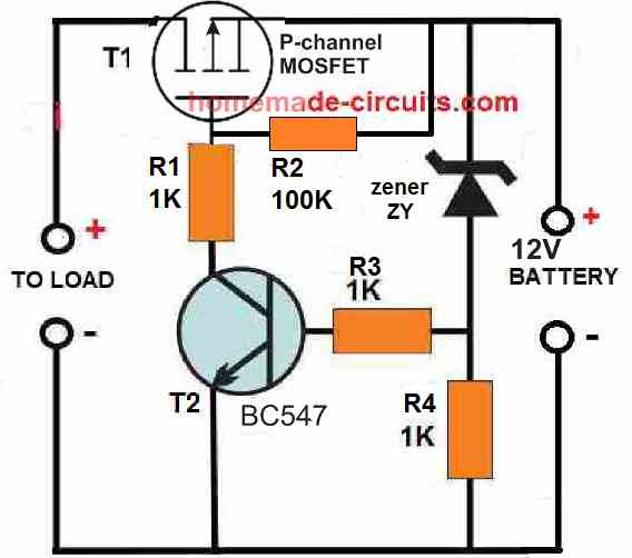
When a MOSFET is used in place of the BJT TIP36, the 50 ohms resistor can be replaced with a 1K resistor or a 10K resistor, and the TIP122 can be replaced with a BC547.
Adding a Battery Charger with a Single Transistor
The above discussed concepts are used to handle the over discharge situation of a connected battery. However, if you want the above circuit to also have its own battery charger, then the following circuit can be used for the process effectively.
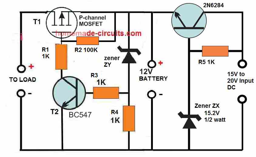
Here we can see a transistor stage on the right side of the design, which is configured as an emitter follower. The transistor is a 2N6284, which is rated to provide at least 10 amp current to the battery, which means it is able to charge even a 100 Ah battery efficiently.
Since the transistor is a Darlington transistor and configured as an emitter follower, the voltage at its emitter will always lag behind its base voltage by 1 V or 1.2 V.
The zener diode must be cautiously selected so that it compensates the emitter drop of 1.2 V by providing a potential at the base which may be 1.2 V higher than the required emitter voltage.
Since the circuit is designed to charge a 12 V battery, the full charge voltage at the emitter of this transistor must be around 14.1 V. This implies that the base voltage of the transistor must be 1.2 V higher than the emitter, which amounts to a value of around 15.2 V to 15.3 V.
This is exactly why the zener must be rated at the above specified voltage for generating a constant 14. 1 V at the emitter side and across the connected 12 V battery.
While charging the battery when the battery terminal voltage reaches the 14.1 V value, it reverse biases the emitter of the 2N6284, which shuts down the conduction of the transistor, thereby stopping any further charging of the battery, and the battery is safeguarded from over charging.
The above shown circuit thus implements a 2 in 1 procedure of preventing battery over deep discharge and also over charging through the use a just a few transistors, and still is able to control a battery that may be as big as a 12 V 100 Ah battery.
Deep Discharge Protection with more Accuracy
In the above 2 BJT concepts, cutoff drifts with load, so when load changes then behavior also shifts. Different transistor gives different cutoff point, since no two devices behave exactly same. Temperature sensitive too, so heat comes then things move. Due to this cutoff feels soft, kind of mushy, not clean break.
However in the following 3 BJT version, cut-off point stays stable, even when conditions change. Behavior is repeatable, so you build again and it works same. Disconnect of load is sharp, clear on and off. Works same with small load or large load, no deviations...
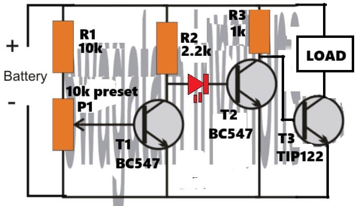
How it Works
This circuit keeps monitoring the battery voltage all the time. If the battery voltage is healthy then the LOAD stays ON and keeps working.
But when battery voltage drops below a preset level then the circuit disconnects the LOAD.
This helps prevent deep discharge, which otherwise damages batteries, especially lead-acid and Li-ion packs without BMS, so that damage part is avoided.
Blocks In The Circuit
The whole circuit can be seen as four simple functional blocks working together.
- First is the voltage sensing network using R1 and P1.
- Then comes the comparator transistor T1 (BC547).
- After that there is the switching or driver stage using T2 (BC547).
- Finally the power switching is handled by T3 (TIP122), which actually controls the LOAD.
Voltage Sensing (R1 + P1)
R1 (10k) and P1 (10k preset) form a voltage divider connected to the battery. The wiper of P1 feeds the base of T1 directly.
So as battery voltage rises or falls, the voltage at T1 base also changes along with it. P1 sets the cutoff voltage, so here you decide when the LOAD should disconnect, like at 10.8 V or 11.0 V and similar values. This part is basically the adjustment control of the whole circuit.
T1 – The Voltage Detector (BC547)
T1 works like a simple comparator here. When battery voltage is HIGH, the voltage at T1 base becomes greater than about 0.6 V, then T1 turns ON and its collector voltage drops toward ground.
When battery voltage becomes LOW, then base voltage of T1 falls below about 0.6 V, then T1 turns OFF and its collector voltage rises through R2.
So T1 converts the battery condition into logic levels, giving a LOW signal when battery is OK and a HIGH signal when battery voltage is low.
T2 – Logic Inverter + Buffer (BC547)
R2 (2.2k) pulls the base of T2 HIGH when T1 is OFF.
When the battery is OK, T1 stays ON, its collector is LOW, so T2 base is LOW and T2 remains OFF. But when battery voltage drops, T1 turns OFF, its collector goes HIGH via R2, then T2 base becomes HIGH and T2 turns ON.
In this way T2 flips the logic and also provides stronger drive for the power transistor.
LED Indicator Role
That LED is doing two jobs at the same time, it gives visual indication because when the battery voltage falls below the preset level, then the LED lights up, and because of that it acts as a LOW BATTERY indicator.
When the battery is OK the LED stays OFF, but when the battery goes LOW then the LED turns ON, simple and very useful in real-world use.
At the same time the LED also works as a reference voltage and level shift. A red LED drops about 1.6 V – 1.8 V, which is much higher and more stable than a normal diode, so because of this T2 does not turn ON immediately. It turns ON only when T1 fully releases the node, and that helps improve cutoff accuracy and noise immunity. In short, the LED creates a clean threshold for T2 switching.
Now looking at how the LED works inside this circuit, when the battery voltage is OK then T1 is ON and the node feeding the LED is pulled LOW, so the LED stays reverse biased and OFF. Because of that T2 remains OFF and TIP122 stays ON, therefore the LOAD remains powered.
But when the battery voltage drops below the preset level, then T1 turns OFF and the node rises via R2. At that point the LED becomes forward biased and lights up, so now the base of T2 gets proper bias and T2 turns ON. Once T2 turns ON, the TIP122 base is pulled LOW and therefore the LOAD disconnects.
T3 – Power Switch (TIP122)
TIP122 is a Darlington transistor, so it has very high gain and can handle high current loads easily. When battery voltage is OK, T2 stays OFF, so the base of TIP122 gets drive and TIP122 turns ON, allowing the LOAD to remain powered.
When battery voltage becomes LOW, T2 turns ON and pulls the base of TIP122 LOW, so TIP122 turns OFF and the LOAD gets disconnected. This is the stage where the actual battery protection happens.