Two main types of FETs that presently exist are: JFETs and MOSFETs.
MOSFETs can be further classified into depletion type and enhancement type. Both these types define the fundamental mode of operation of MOSFETs, while the term MOSFET itself is the abbreviation of metal-oxide-semiconductor-field-effect transistor.
Due to the fact that the two types have different working characteristics, we'll be evaluating each of them separately in different articles.
Difference between Enhancement and Depletion MOSFET
Basically, unlike enhancement MOSFETs, depletion MOSFETs are in an on-state even in the presence of a 0 V across the gate-to-source terminals (VGS).
For an enhancement MOSFET, the gate-to-source voltage (VGS) must be above its gate-to-source threshold voltage (VGS(th)) in order to make it conduct.
However, for an N-channel depletion MOSFET, its VGS(th) value is above 0 V. This means that even if VGS = 0 V, a depletion MOSFET is able to conduct current. To turn it off, the VGS of a depletion MOSFET needs to be reduced below the VGS(th) (negative).
In this present article we'll discuss the depletion type MOSFET, which are said to have characteristics matching that of a JFET. The similarity is between cut-off and saturation near IDSS.
Basic Construction
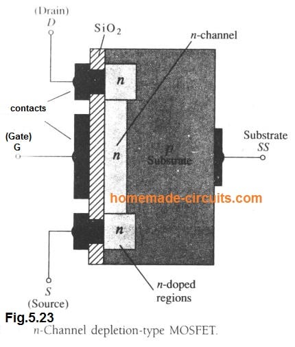
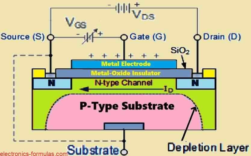
Fig.5.23 shows the basic internal structure of a n-channel depletion-type MOSFET.
We can find a block of p-type material created using a silicon base. This block is called the substrate.
The substrate is the base or the foundation over which a MOSFET is constructed. For some MOSFETs it is internally linked with the "source" terminal. Also, many devices offer an extra output in the form of SS, featuring a 4-terminal MOSFET, as revealed in Fig.5.23
The drain and the source terminals are connected through conductive contacts to n-doped locations, and attached through an n-channel, as indicated in the same figure.
The gate is also connected to a metallic layer, although it is insulated from the n-channel through a fine layer of silicon dioxide (SiO2).
SiO2 possesses a unique form of insulation property called dielectric which creates an opposing electric field within itself in response to an externally applied electric field.
Being an insulating layer, the material SiO2 offers us the following important information:
A complete isolation is developed between the gate terminal and the mosfet channel with this material.
Moreover, it is because of SiO2, the gate of the mosfet is able to feature an extremely high degree of input impedance.
Due to this vital high input impedance property, the gate current IG is virtually zero amps for any dc-biased MOSFET configuration.
Basic Operation and Characteristics
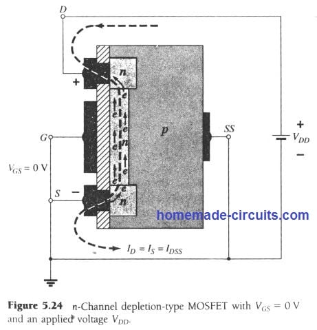
AS can be seen in Fig.5.24, the gate to source voltage has been configured at zero volts by connecting the two terminals together, while a voltage VDS is applied across the drain and source terminals.
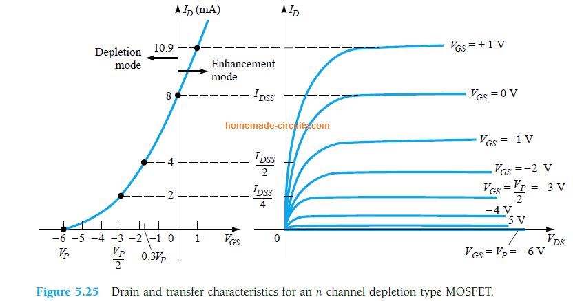
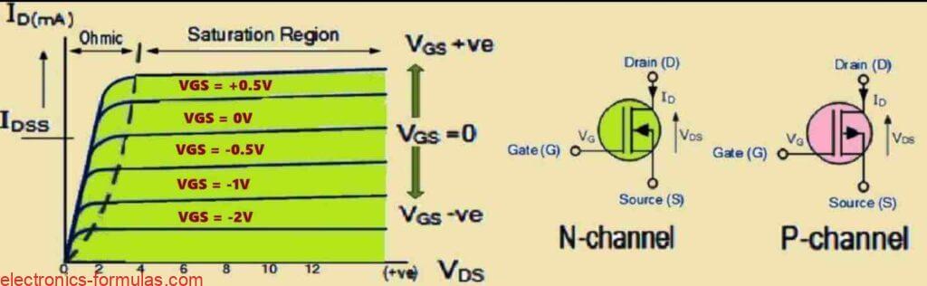
With the above setting, the drain side establishes a positive potential by the n-channel free electrons, along with an equivalent current through the JFET channel. Also, the resulting current VGS = 0V is still being identified as IDSS, as given in Fig. 5.25
We can see that in Fig.5.26 the gate source voltage VGS is given a negative potential in the form of -1V.
This negative potential tries to force electrons toward the p-channel substrate (since charges repel), and pull holes from the p-channel substrate (since opposite charges attract).
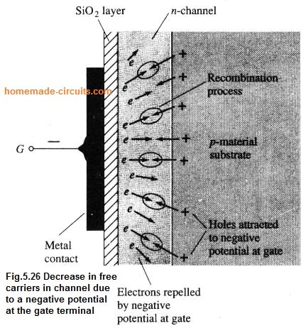
Depending on how large this negative bias VGS is, a recombination of holes and electrons takes place which results in the reduction of free electrons in the n-channel available for the conduction. Higher levels of negative bias results in higher rate of recombination.
The drain current consequently is reduced as the above negative bias condition is increased, which is proven in Fig.5.25 for VGS levels of VGS = -1, -2 and so forth, until the pinch-off mark of -6V.
The drain current as a result along with the transfer curve plot proceeds just like that of a JFET.
Now, for the positive VGS values, the gate positive will attract excess electrons (free carriers) from the p-type substrate, on account of the reverse leakage current. This will establish fresh carriers by the way of resultant collisions across the accelerating particles.
As the gate-to-source voltage tends to rise at the positive rate, the drain current shows a rapid increase, as proven in the Fig.5.25 for the same reasons as discussed above.
The gap developed between the curves of VGS = 0V and VGS = +1 distinctly shows the amount by which the current increased due to the 1 - V variation of the VGS
Due to the fast rise of the drain current we must be careful about the maximum current rating, otherwise it could cross the positive gate voltage limit.
For example, for the device type depicted in the Fig.5.25, applying a VGS = +4V would cause the drain current to rise at 22.2 mA, which may be crossing the maximum breakdown limit (current) of the device.
The above condition shows that the use of a positive gate-to-source voltage generates an enhanced effect on the quantity of the free carriers in the channel, as opposed to when VGS = 0V.
This is why the positive gate voltage region on the drain or transfer characteristics is generally known as enhancement region. This region lies between the cut-off and the saturation level of IDSS or the depletion region.
Solving an Example Problem
Advantages and Applications
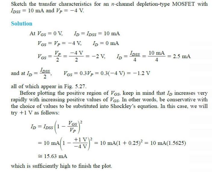
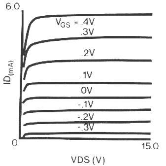
In contrast to enhancement-mode MOSFETs, where we find the drain current dropping to zero in response to a zero gate-to-source voltage, the modern depletion-mode FET features noticeable current with zero gate voltage. To be precise, the drain-to-source resistance is usually 100 Ohms in zero voltage.
As indicated in the above graph, the ON-resistance rds(on) vs analogue signal range looks like a practically flat response. This characteristic, in conjunction with the low-capacitance levels of the these advanced depletion type device, allow them to be specifically ideal as analogue switches for audio and video switching applications.
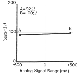
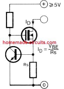
The depletion-mode MOSFET's 'normally-on' attribute enables the device to be perfectly suitable for single FET current regulators.
One such example circuit can be seen in the following figure.
The Rs value could be determined using the formula:
Rs = VGSoff [ 1 - ( ID/IDSS)1/2] / ID
where ID is the amount of regulated current required at the output.
The main advantage of depletion-mode MOSFETs in current-source application is their minimal drain capacitance, that makes them appropriate for biasing applications in low-input leakage, medium-speed (>50 V/us) circuits.
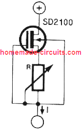
The figure below exhibits a low-input-leakage current differential front-end using a double low-leakage function FET.
Generally speaking, either side of the JFET is going to be biased at ID = 500 uA. Therefore, the current obtainable for charging compensation and stray capacitances becomes restricted to 2ID or, in cases like this, 1.0 mA. The JFET's corresponding features are production-proven and assured on the datasheet.
Cs symbolizes the output capacitance of the input stage 'tail' current source. This capacitance is crucial in non-inverting amplifiers, due to the fact that the input stage experiences significant signal exchanges throughout this network, and the charging currents in Cs could be big. In case normal current sources are employed, this tail capacitance could be accountable for noticeable slew-rate deterioration in non-inverting circuits (compared to inverting applications, where the charging currents in Cs tend to be minimal).
The drop in the slew-rate could be expressed as:
1 / 1+ (Cs/Sc)
So long as Cs is lower than Cc (the compensation capacitor), there may be hardly any variation in the slew rate. Working with the DMOS FET, Cs can be around 2 pF. This strategy produces a huge improvement in the slew-rate. Where current deficits higher than 1 to 5 mA are needed, the device could be biased into the enhancement mode to generate as much as 20 mA for a maximum VGS of +2.5 V, with minimal output capacitance continuing to be a key aspect.
The next application below exhibits a proper enhancement-mode current source circuit.
A 'normally-on' analogue switch could be built for requirements where standard condition becomes necessary during a supply voltage failure, for example in automatic ranging of test tools or for ensuring accurate start-up of logic circuits at switch ON.
The reduced negative threshold voltage of the device offers basic drive prerequisites and permits working with minimal voltage.
The circuit below demonstrates the common bias factors for any depletion-mode DMOS analogue switch.
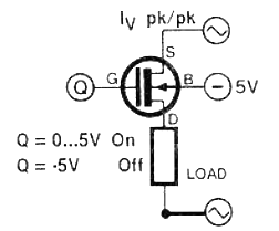
To cause the device to switch off, a negative voltages becomes necessary on the gate. Having said that, the on-resistance could be minimized when the FET is additionally enhanced using a positive gate voltage, enabling it specifically in the enhancement-mode region along with the depletion-mode region.
This response can be witnessed in in the following graph.
The high-frequency gain of the unit, together with its low capacitance values, delivers an increased 'figure of merit'. It is really an crucial element in VHF and UHF amplification, which specifies the gain-bandwidth product (GBW) of the FET, which could be depicted as:
GBW = gfs / 2π(Cin + Cout)
p-Channel Depletion-Type MOSFET
The construction of a p-channel depletion-type MOSFET is a perfect reverse of an n-channel version shown in Fig.5.23. Meaning, the substrate now takes the form of an n-type and the channel becomes a p-type, as can be seen in Fig.5.28a below.
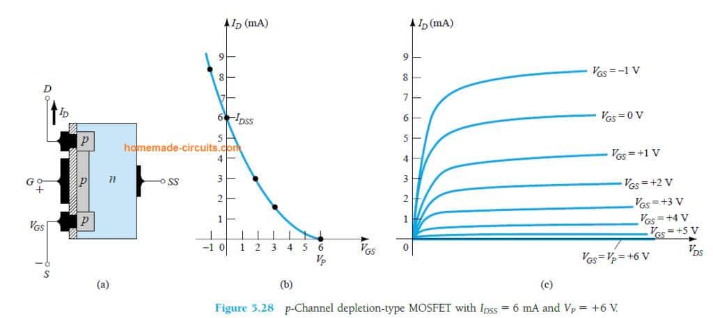
The terminal identification remains unchanged, but the voltage and the current polarities are reversed, as indicated in the same figure. The drain characteristics would be exactly as depicted in Fig.5.25, except VDS sign which will in this case get a negative value.
The drain current ID shows a positive polarity in this case too, that's because we have already reversed its direction. VGS shows an opposite polarity, which is understandable, as indicated in Fig.5.28c.
Because VGS is reversed produces a mirror image for the transfer characteristics as indicated in Fig.5,28b.
Meaning, the drain current increases in the positive VGS region from the cut-off point at VGS = Vp until IDSS, then it continues to rise as the negative value of VGS rises.
Symbols
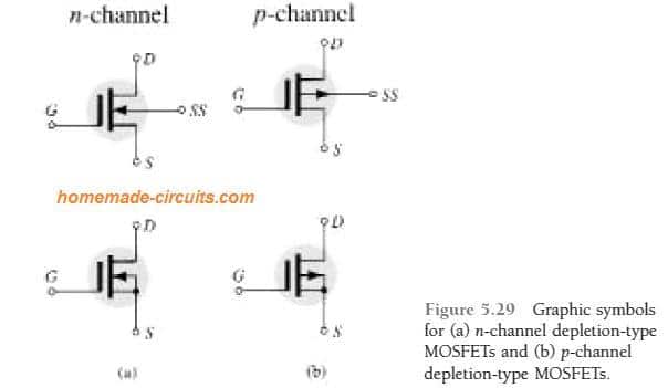
The graphical signs for an n- and p-channel depletion-type MOSFET can be witnessed in the above Fig. 5.29.
Observe the way the selected symbols aim to represent the true structure of the device.
The absence of a direct interconnection (because of the gate insulation) between the gate and channel is symbolized by a gap between the gate and the different terminals of the symbol.
The vertical line which represents the channel is attached between the drain and source and is “held” by the substrate.
Two groups of symbols are furnished in the figure above for each type of channel to highlight the fact that in some devices the substrate may be accessible externally while in others this may not be seen.
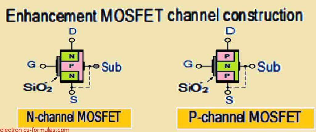
MOSFET (Enhancement-Type)
Although depletion type and enhancement type MOSFETs look similar with their internal structures and functional mode, their characteristics may be quite different.
The main difference being the drain current which depends on a specific level of gate-to-source voltage for the cut off action.
Precisely, an n-channel enhancement-type MOSFET can work with a positive gate/source voltage, instead of a range of negative potentials which can normally impact a depletion type MOSFET.
Basic Construction
You can visualize the n-channel enhancement-type MOSFET in the following
Fig. 5.31.
A p-type material section is created through a silicon base, and as learned before it is termed as the substrate.
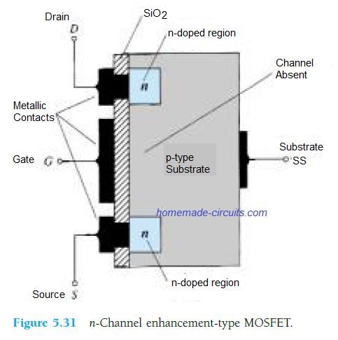
This substrate on some occasions is attached internally with the source pin in a depletion-type MOSFET, while in some instances it is terminated as a fourth lead for enabling an external control of its potential level.
The source and drain terminals are as usual joined using metallic contacts to n-doped regions.
However, it may be important to visualize that in Fig. 5.31 the channel between the two n-doped regions is missing.
This may be considered as the fundamental dissimilarity between a depletion-type and an enhancement-type MOSFET's internal layout, that is an absence of an inherent channel which is supposed to be a part of the device.
The SiO2 layer can be seen still prevalent, which ensures an isolation between the metallic base of the gate terminal and the region between the drain and source. However, here it can be witnessed standing separated from the p-type material section.
From the above discussion we can conclude that a depletion and enhancement MOSFET internal layout may have some similarities, except the missing channel between drain/source for an enhancement type of MOSFET.
Basic Operation and Characteristics
For an enhancement type MOSFET when a 0 V is introduced at its VGS, due to the missing n-channel (which is known to carry a lot of free carriers) causes a current output to be zero, which is quite unlike of a depletion type of MOSFET, having ID = IDSS.
In such a situation due to a missing path across drain/source terminals, large amounts of carriers in the form of electrons are unable to accumulate at drain/source (because of the n-doped regions).
Applying some positive potential at VDS, with VGS set at zero volts and the SS terminal shorted with the source terminal, we actually find a couple of reverse biased p-n junctions between the n-doped regions and the p-substrate to enable any notable conduction across drain to source.
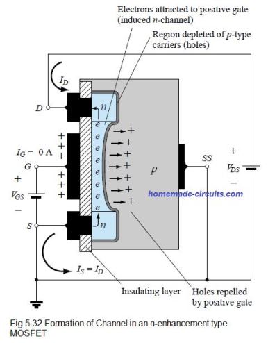
In Fig. 5.32 shows a condition where VDS and VGS are applied with some positive voltage higher than 0 V, allowing the drain and gate to be at a positive potential with respect to the source.
The positive potential at the gate pushes the holes in the p-substrate along the edge of the SiO2 layer departing the location and entering deeper into the regions of the p-substrate, as shown in the above figure. This happens because of the like charges that repel each other.
This results in a depletion region being created close to the SiO2 insulating layer that is void of holes.
Despite of this, the p-substrate electrons which are the minority carriers of the material are pulled towards the positive gate and start gathering in the region close to the surface of the SiO2 layer.
Due to the insulation property of the SiO2 layer negative carriers allow the negative carriers from getting absorbed at the gate terminal.
As we increase the level of VGS, the electron density close to the SiO2 surface also increase, until finally the induced n-type region is able to allow a quantifiable conduction across drain/source.
The VGS magnitude that causes an optimal increase in the drain current is termed as the threshold voltage, signified by the symbol VT. In datasheets you will be able to see this as VGS(Th).
As learned above, due to the absence of a channel at VGS = 0, and "enhanced" with the positive gate-to-source voltage application, this type of MOSFET are known as enhancement-type MOSFETs.
You will find that both depletion- and enhancement-type MOSFETs exhibit enhancement-type regions, but the term enhancement is used for the latter because it specifically works using an enhancement mode of operation.
Now, when VGS is pushed over the threshold value, the concentration of the free carriers will boost in the channel where it's induced. This causes the drain current to increase.
On the other hand, if we keep the VGS constant and increase the VDS (drain-to-source voltage) level, this will ultimately cause the MOSFET to reach its saturation point, as normally would also happen to any JFET or a depletion MOSFET.
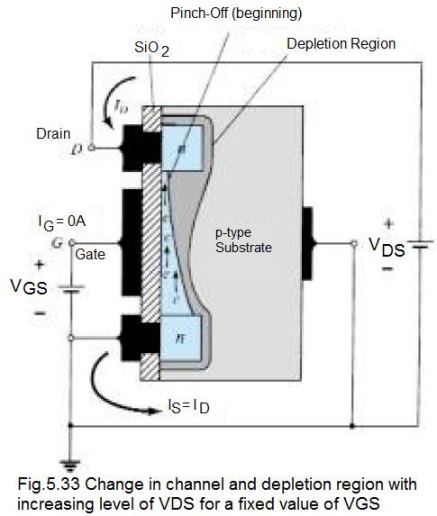
As shown in Fig. 5.33 the drain current ID gets leveled off with the aid of a pinching-off process, indicated by the narrower channel towards the drain end of the induced channel.
By applying applying Kirchhoff’s voltage law to the MOSFET's terminal voltages in Fig. 5.33, we get:
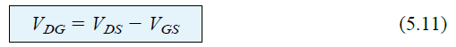
If VGS is kept constant to a specific value, for example 8 V, and VDS is raised from 2 to 5 V, the voltage VDG by Eq. 5.11 could be seen dropping from -6 to -3 V, and the gate potential getting less and less positive with respect to the drain voltage.
This response prohibits the free carriers or electrons from getting pulled towards this region of the induced channel, which in turn results in a drop in the effective width of the channel.
Ultimately, the channel width decreases to the point of pinch-off , reaching a saturation condition similar to what we already learned in our earlier depletion MOSFET article.
Meaning, increasing the VDS any further with a fixed VGS does not affect the saturation level of ID, until the point where a breakdown situation is reached.
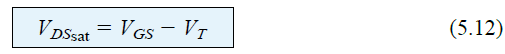
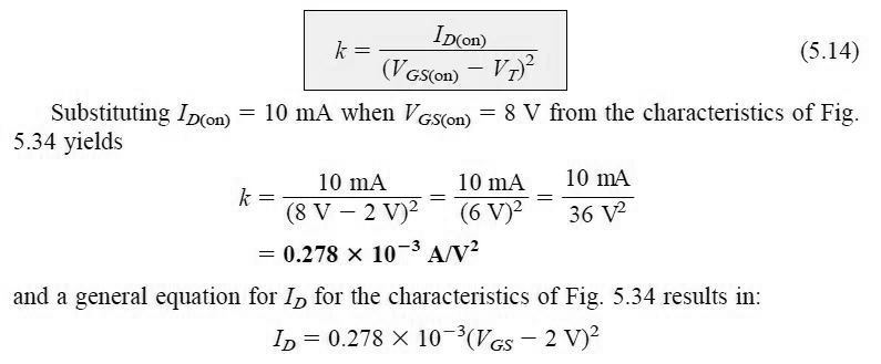
Looking at the Fig 5.34 we can identify that for a MOSFET as in Fig.5.33 having VGS = 8 V, saturation takes place at a VDS level of 6 V. To be precise the VDS saturation level is associated to the applied VGS level by:
No doubt, it thus implies that when the VT value is fixed, increasing the level of VGS will proportionately cause higher levels of saturation for VDS through the locus of saturation levels.
Referring to the characteristics shown in the above figure, the VT level is 2 V, which is evident by the fact that the drain current has fallen to 0 mA.
Therefore typically we can say:
When VGS values are less than the threshold level for enhancement-type MOSFET, its drain current is 0 mA.
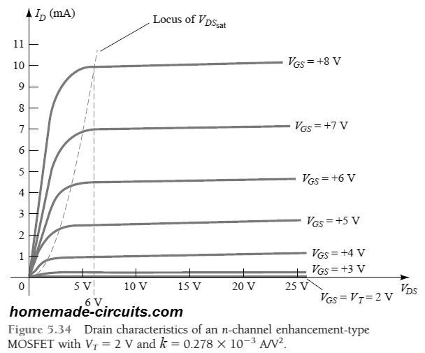
We can also clearly see in the above figure that as long as the VGS is raised higher from VT to 8 V, the corresponding saturation level for ID also increases from 0 to 10 mA level.
Moreover we can further notice that the space between the VGS levels increases with an increase in the value of VGS, causing an infinitely rising increments in drain current.
We find the drain current value is related to the gate-to-source voltage for VGS levels that's greater than VT, through the following nonlinear relationship:
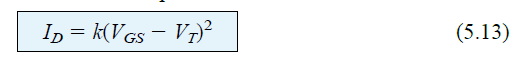
The term which is shown squared bracket is the term which is responsible for the nonlinear relatinship between ID and VGS.
The term k is a constant and is a function of the MOSFET layout.
We can find out the value of this constant k through the following equation:
where the ID(on) and VGD(on) each are values specifically depending on the characteristic of the device.
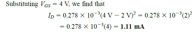
In the next Fig. 5.35 below we find the drain and transfer characteristics are arranged one beside the other to clarify the transfer process across one another.
Basically, it is similar to the process explained previously for JFET and depletion-type MOSFETs.
However, for the present case we have to remember that the drain current is 0 mA for VGS VT.
Here ID may see a noticeable amount of current, which will increase as determined by Eq. 5.13.
Note, while defining the points over the transfer characteristics from the drain characteristics, we only consider the saturation levels. This restricts the region of operation to VDS values higher than the saturation levels as established by Eq. (5.12).
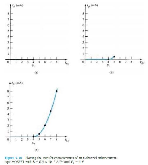
p-Channel Enhancement-Type MOSFETs
The structure of a p-channel enhancement-type MOSFET as shown in Fig. 5.37a is just the opposite of that showing up in Fig. 5.31.
Meaning, now you find that an n-type substrate and p-doped regions beneath the drain and source joints.
The terminals continue to be as established, but each of the current directions and the voltage polarities are reversed.
The drain characteristics can look like as given in Fig. 5.37c, having increasing amounts of current caused by a continuously more negative magnitudes of VGS.
The transfer characteristics would be the mirror impression (around the ID axis) of the transfer curve of Fig. 5.35, having ID increasing with more and more negative values of VGS above VT, as displayed in Fig. 5.37b. Equations (5.11) through (5.14) are similarly appropriate to p-channel devices.
Additional Useful Information Regarding Depletion Type, Enhancement Type FETs
Now in this section we will further discuss deeply about Field Effect Transistor (FET). This one is not the Junction Field Effect Transistor (JFET) that you already know.
This device we call Metal Oxide Semiconductor Field Effect Transistor (MOSFET). It is also called Insulated Gate Field Effect Transistor (IGFET).
Why MOSFET Is Special
MOSFET is very special semiconductor device because its gate input is fully separated from main current carrying channel. So this gives big advantage in many applications.
MOSFET is used in many electronic circuits because of this special construction. In fact, MOSFET is most common type of insulated gate FET. This is mainly because it is very versatile and very effective in many conditions.
Inside The MOSFET
Inside MOSFET we see that the Gate is separated from main n-channel or p-channel by one very thin insulating layer. This material is usually silicon dioxide and you may also know it as glass.
This insulating layer makes electrical insulation. Because of that we call it “Metal Oxide” Gate electrode.
We can think this very thin insulated metal Gate electrode is like one plate of a capacitor.
High Input Resistance
Because of this design the controlling Gate is electrically isolated. So MOSFET gets very high input resistance, sometimes in Mega-ohms range, which looks almost like infinity.
This feature is very important in MOSFET working. It makes MOSFET different from JFET and makes it work like voltage controlled device with insulated Gate.
Current Flow In MOSFET
As we know, the gate of MOSFET is electrically isolated from main path between Drain and Source. So then no current can flow into gate.
Same like JFET, the MOSFET also works like voltage controlled resistor.
So this means current flowing through channel between Drain and Source depends directly on input voltage which we apply at Gate.
Static Charge Problem
Same like JFETs, MOSFETs also have very high input resistance. So they can collect large static charge.
Because of this MOSFET can get damaged very easily if we do not handle them carefully or if we do not protect them.
Terminals Of MOSFET
Same like JFETs, MOSFETs also have three terminals. These are Gate, Drain and Source.
In this family we have two types: P-channel MOSFET (PMOS) and N-channel MOSFET (NMOS). We can use them in different applications as needed.
Two Types Of MOSFET
But now we must understand that MOSFETs are of two main types.
Depletion Type: This type needs one specific Gate-Source voltage (VGS) to switch device OFF. We can compare it with one switch that is Normally Closed.
Enhancement Type: This type needs Gate-Source voltage (VGS) to switch device ON. We can compare it with one switch that is Normally Open.
Below are the symbols and fundamental construction for both the MOSFET variants.
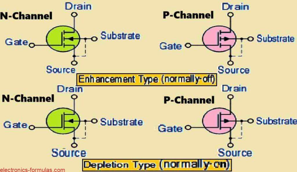
Substrate Terminal In MOSFET
Now when we see the four MOSFET symbols shown above, we also see one extra terminal and this is called Substrate. We must note that this Substrate is not normally used as input or output connection.
So its main job is to work like grounding point for the substrate and we have to remember this.
This Substrate makes a connection to main semiconductive channel through a diode junction and that junction links to the body or metal tab of the MOSFET, so you can imagine that.
Substrate Connected To Source
Now in most discrete MOSFET, this Substrate lead is already connected inside to the Source terminal. So, when this internal connection exists and especially in enhancement type MOSFET then we do not show the Substrate in the symbol, so it looks simple and clear.
Channel Line In MOSFET Symbol
Inside the MOSFET symbol, the line which goes between the Drain (D) and the Source (S) is showing the semiconductive channel of the transistor.
Now when this channel line is solid and not broken, then it means it is Depletion mode MOSFET, that is normally ON, so drain current can flow even when there is no Gate bias potential.
But when this channel line is dotted or broken, then it means it is Enhancement mode MOSFET, that is normally OFF so zero drain current will flow when there is no Gate potential applied.
Arrow Direction And Channel Type
Also we must check the arrow which points toward the channel line, because it tells us whether the conductive channel is made from P-type material or from N-type material.
Fundamental Structure and Symbol of a MOSFET
How MOSFET Is Different
Now when we investigate the Metal Oxide Semiconductor Field Effect Transistor (MOSFET), we see that it is very different from Junction Field Effect Transistor (JFET).
In both Depletion and Enhancement MOSFET, we control flow of charge carriers by electric field which comes from gate voltage.
So in n-channel MOSFET, the electrons are moving, but in p-channel MOSFET, the holes are moving. The change happens inside semiconductive channel which is between drain and source terminals.
A MOSFET has one gate electrode which is kept on top of very thin insulating layer. Under this layer, we see two very small n-type areas below the drain and source electrodes.
This full arrangement is very important because without this structure the device cannot work.
Why MOSFET Gate Is Special
In last tutorial we explained how we bias the gate of Junction Field Effect Transistor (JFET) so that it reverse-biases the pn-junction.
But in insulated gate MOSFET, such limits do not apply. This gives us flexibility. So we can bias the gate of MOSFET with positive (+ve) or with negative (-ve) voltage and this makes MOSFET more useful.
Because of this special nature, MOSFET is very good for use like electronic switch or making logic gates. In many cases, when there is no bias, these devices normally do not conduct.
Also MOSFET is voltage-controlled device, so its gate input resistance is very high and it needs very little or almost no control current for working.
Now we see that p-channel and n-channel MOSFET come in two major types: enhancement and depletion. This gives us choice so we can select the right type for our application. That is why MOSFET is very versatile in modern electronics.
Understanding The Depletion-Mode MOSFET
Now when we analyze MOSFET, we find Depletion-mode MOSFET. This type is less common than Enhancement-mode, but it has special features.
This MOSFET is normally "ON". That means it is conducting even when there is no gate bias voltage.
So in this case we can see that channel keeps conducting when gate-source voltage (VGS) is zero. That shows it is a "normally-closed" device. The circuit symbol of depletion MOS transistor shows solid channel line which means channel is normally closed and conducting.
Now let us see n-channel depletion MOS transistor. When we supply negative gate-source voltage (-VGS), then the free electrons inside channel reduce, so channel gets depleted and transistor becomes "OFF". This is how the name depletion-mode comes.
In the same way, when we study p-channel depletion MOS transistor, we see that positive gate-source voltage (+VGS) removes free holes from channel, so it becomes "OFF".
If we talk in other way, then in n-channel depletion-mode MOSFET, if we apply positive gate-source voltage (+VGS), then electrons inside channel increase, so more current flows. But when we apply negative gate-source voltage (-VGS), then electrons reduce and current also reduces.
For p-channel type it is same rule but in reverse manner.
So finally we may compare depletion-mode MOSFET to a "normally-closed" switch. This shows that its different working style in electronic circuits.
Circuit Symbols of Depletion-mode N-Channel MOSFET
Now let us see how depletion-mode MOSFET is built. The construction of depletion-mode MOSFET is almost same as JFET transistors, so we can compare both. In this type, the drain-source channel already has conduction and this is because of electrons and holes present inside n-type or p-type channel.
The doping in the channel makes a pathway with low resistance between Drain and Source and this happens even when there is no Gate bias, so current can already move.
Understanding The Enhancement-Mode MOSFET
Now let us go ahead and understand another type, which is enhancement-mode MOSFET and many people call it eMOSFET also. This type is more popular and widely used, but it works in opposite way compared to depletion-mode type.
In enhancement-mode MOSFET, the channel is weakly doped or sometimes fully undoped, so in normal condition it is non-conductive. Because of this the device stays OFF when gate bias voltage VGS is zero. The circuit symbol of enhanced MOS transistor also shows this with broken channel line, so it means the channel is normally open and non-conductive.
N-Channel Enhancement MOSFET
Now in case of n-channel enhancement MOS transistor, we see that drain current starts to flow only when we apply a gate voltage VGS which is higher than one particular threshold voltage VTH. This threshold voltage tells us the exact point where conductance begins, so we call this device a transconductance device.
Now the moment we put positive gate voltage (+VGS) to an n-type eMOSFET, it pulls more electrons toward oxide layer around the gate. So at this time the channel thickness increases, or we can say it is enhanced and this allows bigger current to flow. This is why we call it enhancement-mode device because gate voltage improves the channel and makes it more conductive and this also gives better efficiency in electronic applications.
Now when we increase positive gate voltage in n-channel enhancement-mode MOSFET, then the channel resistance goes down. Since the resistance goes down, then drain current ID increases through the channel.
So in simple words, in n-channel enhancement-mode MOSFET, a positive gate-source voltage +VGS turns transistor ON but zero or negative gate-source voltage -VGS keeps it OFF. Because of this we can compare enhancement-mode MOSFET with a normally-open switch, since it needs certain gate voltage to start conduction.
P-Channel Enhancement MOSFET
But now let us see the opposite type, which is p-channel enhancement MOS transistor. Here also, whenever gate-source voltage VGS is zero, then the device remains OFF and channel stays open.
The moment we apply a negative gate voltage -VGS to a p-type eMOSFET, then the channel conductivity increases, so the transistor turns ON.
So for p-channel enhancement-mode MOSFET, a positive gate-source voltage +VGS turns transistor OFF and a negative gate-source voltage -VGS turns transistor ON.
This special way of working shows us how enhancement-mode MOSFETs are versatile and useful in many different electronic circuits.
Circuit Symbols of Enhancement-mode N-Channel
How Enhancement-Mode MOSFET Works As Switch
Now let us see about Enhancement-mode MOSFET. We can consider them as very efficient electronic switches.
This happens because they have very low ON resistance and they also have very high OFF resistance, so they can pass or block current very strongly.
Also we cannot forget that they have infinitely high input resistance. This happens because of their isolated gate structure, so no current flows inside gate.
So we can see that Enhancement-mode MOSFET becomes very useful in integrated circuits and we use them in real world.
Use In CMOS
Now in CMOS logic gates we use both PMOS and NMOS and they do logical operations together.
The word CMOS means Complementary MOS, so it shows us that we are using both PMOS and NMOS transistors in one design.
This complementary style makes circuit more powerful, more efficient and more flexible, so we can use them in many different electronic applications.
Understanding The MOSFET As Amplifier
Now let us also see how MOSFET can work as amplifier. Just like JFET, we can use MOSFET to make single-stage Class A amplifier circuits.
Among these, enhancement-mode n-channel MOSFET common source amplifier works best and it is used the most.
Now even though depletion-mode MOSFET amplifier looks similar to JFET amplifier, we must remember that MOSFET has much higher input impedance.
This high input impedance is mainly decided by gate biasing resistive network and this network is made using resistors R1 and R2.
Now let us also remember one important point. The output signal from enhancement-mode common source MOSFET amplifier becomes inverted.
So when gate voltage VG is low, then transistor becomes OFF and then output voltage VD or Vout becomes high.
But on the other side, when gate voltage VG is increased then transistor becomes ON and then output voltage VD or Vout becomes low.
Analyzing an Enhancement-mode N-Channel Amplifier Circuit
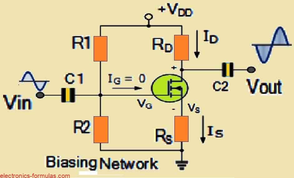
- VG = [R2/(R1 + R2)]VDD
- ID = VS/RS
DC Biasing Of Common Source MOSFET Amplifier
Now when we look at the DC biasing of the common source MOSFET amplifier circuit, we find that it looks very similar to the biasing method we use in JFET amplifier, so we can compare both.
In this arrangement, we make the biasing in Class A mode and we do this by making a voltage divider network with resistors R1 and R2, so we can fix the correct operating point of amplifier.
Now we can also see that the AC input resistance of the common source MOSFET amplifier is RIN = RG = 1 MΩ. This is very high input resistance and it is good because it reduces the loading effect on the earlier stage in the circuit.
MOSFET Basic Nature
Now MOSFET is a Metal Oxide Semiconductor Field Effect Transistor and it is a three-terminal active device.
These devices are made using special semiconductor materials and that gives them unique ability that they can act like insulator or they can act like conductor and that depends on the small signal voltage which we apply.
Because of this unique property, MOSFET can move between two different states, so it can do two main jobs. One is switching in digital electronics and the other is amplification in analog electronics.
Now MOSFET can do this in three regions and each region has its own voltage condition, so let us see them step by step.
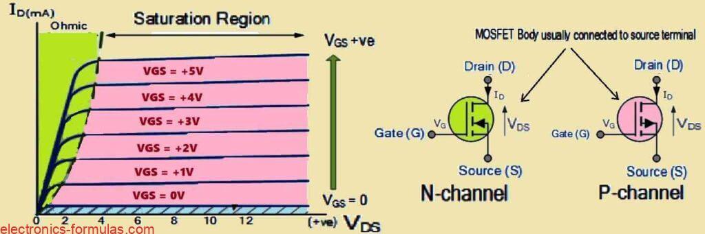
Cut-Off Region
In cut-off region when VGS is less than Vthreshold, then we find that gate-source voltage is much lower than transistor threshold voltage.
So as a result, MOSFET becomes fully OFF and drain current ID becomes zero. In this state, the transistor works like an open switch and this is true regardless of the value of drain-source voltage VDS.
Linear Or Ohmic Region
Now in this region when VGS is more than Vthreshold but VDS is less than VGS, then the MOSFET goes in linear or constant resistance area.
So in this case, MOSFET behaves like voltage controlled resistor and its resistance value is set by the gate voltage VGS. This gives us very fine control over current flow, so it is useful.
Saturation Region
Now once VGS reaches Vthreshold and VDS becomes more than VGS, then the MOSFET moves into saturation region.
Here the transistor works like continuous current source and it is fully ON. The drain current ID reaches the highest value possible. In this condition, MOSFET behaves like closed switch, so it allows maximum current to flow.
Important Conclusions
Now we know that MOSFET is famous because it has very high input gate resistance. This property makes the gate voltage control the current across the source and drain channel very efficiently.
But we must be careful, since this high input impedance and high gain also makes MOSFET very sensitive to static electricity. So, if we do not handle or protect it properly, then it can get damaged easily.
Because of all these advantages, MOSFET is best for working as electronic switch or as common source amplifier. Also power consumption of MOSFET is very low, so it is very efficient.
So typical use of MOSFET we can see in microprocessors, memory systems, calculators, CMOS logic gates and many more circuits.
MOSFET Symbol Understanding
When we check the symbols of MOSFETs, we can see that if the symbol has dotted or broken line inside, then it means it is normally OFF enhancement type. That means when VGS is zero then there is no current through the channel.
But if the symbol shows continuous line, then it means it is normally ON depletion type. That shows that current can flow through the channel even when the gate voltage is zero.
Now for p-channel MOSFET, the symbols look same for both types but here the arrow is pointing outward. This makes it easy to identify them and we can also summarize their working in a switching table.
| MOSFET type | VGS = +ve | VGS = 0 | VGS = -ve |
| N-Channel Depletion | ON | ON | OFF |
| N-Channel Enhancement | ON | OFF | OFF |
| P-Channel Depletion | OFF | ON | ON |
| P-Channel Enhancement | OFF | OFF | ON |
Understanding N-Type Enhancement-Mode MOSFET
Now let us see the case of n-type enhancement-mode MOSFET. We find that if we apply a positive gate voltage then the transistor turns “ON” and this allows current to flow through the channel so it becomes conducting.
But since if we apply a zero voltage at the gate then the transistor stays in switched “OFF” state, so no current can pass through the device and it blocks the flow.
Understanding P-Channel Enhancement-Mode MOSFET
Now in the same way for p-channel enhancement-mode MOSFET also, we see that if we apply a negative gate voltage then the transistor switches “ON” and current can pass through the channel.
But if we apply zero gate voltage then the transistor goes into “OFF” state and no current flows, so it remains blocked.
Threshold Voltage
Now the exact point where the MOSFET starts to conduct current through the channel is called the threshold voltage VTH and this value is very important because it decides the operation of the device.
References:
Depletion and enhancement modes
https://en.wikipedia.org/wiki/MOSFET
https://hi.wikipedia.org/wiki/%E0%A4%AE%E0%A5%89%E0%A4%B8%E0%A4%AB%E0%A5%87%E0%A4%9F