In this post I will explain how to build and test a homemade yet very professional looking high power EV battery charger circuit using H-bridge fixed-frequency AC inverter topology, driving a series-resonant LC tank.
Let us go through the step by step working of the circuit stages and other important details:
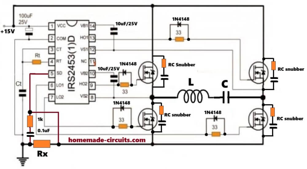
Transmitter Circuit Diagram
The Transmitter or the Wireless EV Battery Charger Coil
You can calculate the value using this Calculator Tool
This transmitter is a full H-bridge fixed-frequency AC inverter driving a series-resonant LC tank where L and C are in series.
The idea here is to generate high-frequency AC and feed it into a resonant primary coil so the LC tank develops high circulating current and energy can be transferred magnetically to the receiver coil.
This circuit is not ZVS, it is actually a forced-drive resonant H-bridge, so timing matters (deadtime adjustment), snubbers matter, and shutdown protection also is mandatory.
Power Supplies Used
There are two different power domains used here. One is the control supply at +15 V which feeds the IRS2453 and also feeds the gate driver bootstrap circuits, and this supply is isolated from the coil power.
That is why you see a 100 µF capacitor near VCC and 10 µF bootstrap capacitors on VB1–VS1 and VB2–VS2. The second supply is the DC bus for the H-bridge which is the high power coil source, it can be 48 V, 96 V, 160 V depending on design, and it feeds the drains of all four MOSFETs. This DC bus is what gets converted into high-frequency AC across the LC tank.
IRS2453 Working
The IRS2453 is doing only one main job which is generating four complementary gate signals with dead-time for a full H-bridge.
Internally it creates LO1 and HO1 for the left half-bridge and LO2 and HO2 for the right half-bridge, so electrically diagonal MOSFET pairs switch alternately and an AC voltage appears across the bridge output nodes.
Oscillator Section Rt And Ct
The RT and CT pins set the switching frequency and this frequency must match the LC resonant frequency.
So first you calculate the LC resonance using our EV calculator and then you choose RT and CT such that the IRS2453 oscillates at that same frequency.
This way the H-bridge excites the LC tank at resonance, current rises naturally, and reactive losses stay low.
Shutdown SD Pin And Protection
The Rx resistor senses excessive current indirectly and when the voltage across Rx rises beyond the threshold then the SD pin is driven high and the IRS2453 shuts down both half-bridges instantly. This protects the MOSFETs, the LC tank, and the DC bus supply.
The RC filter on the SD pin using 1 k and 0.1 µF is very important. One end of the 1 k resistor goes to the SD pin, the other end goes to the sensing node from Rx, and from the SD pin to COM a 0.1 µF capacitor is connected.
This filters noise spikes, prevents false shutdown from switching noise, and allows only real over-current events to trigger shutdown.
Gate Drive Network 33 Ω And Diode
Each MOSFET gate uses a 33 Ω resistor in series and a 1N4148 diode in parallel with that resistor. The resistor limits gate charging current while the diode allows faster discharge or charge depending on orientation, improving switching symmetry and reducing cross-conduction risk.
At these frequencies this network is mandatory.
Bootstrap Capacitors VB–VS
Each high-side MOSFET needs its gate driven above the DC bus, which is why there is a 10 µF capacitor between VB1–VS1 and another 10 µF between VB2–VS2, with 1N4148 diodes charging these capacitors from VCC. Without these bootstrap components the high-side MOSFETs will not turn ON properly.
Full H-Bridge MOSFET Arrangement
Four MOSFETs are arranged in a classic H-bridge where the upper two are high-side and the lower two are low-side.
In one cycle the upper-left MOSFET and lower-right MOSFET turn ON so current flows through the LC tank in one direction, and in the next cycle the upper-right MOSFET and lower-left MOSFET turn ON so the current reverses direction. Because of this the LC tank sees pure AC and not pulsed DC.
LC Tank Connection Very Important
The LC tank is connected in series with coil L in series with capacitor C, and the entire LC network connected between the two bridge midpoints.
This is critical because at resonance the impedance becomes minimum, the current becomes very high, voltage across L and C individually becomes large and a strong magnetic field is produced in the coil. This behavior is exactly what wireless power transfer needs.
RC Snubbers Across MOSFETs
Each MOSFET has an RC snubber connected from drain to source. These snubbers absorb voltage spikes caused by coil leakage inductance, limit dv/dt and protects the MOSFETs during hard switching. Since this design is not ZVS, snubbers are mandatory.
Why This Works Well For Wireless Charging
This transmitter produces controlled AC at a fixed frequency and drives the LC tank at resonance, generating a strong alternating magnetic field with stable frequency.
Power can be controlled using the DC bus voltage or duty control, and it pairs well with a resonant receiver coil followed by a synchronous or diode rectifier and a DC-DC charger stage, as explained below.
Receiver Coil and the Charger Circuit
Receiver Coil (Secondary Coil)
You can calculate the value using this Calculator Tool
Use a flat spiral coil, similar to transmitter coil, but keep it a bit smaller. Diameter can be little less, turns also fewer, but inductance same as transmitter coil...
Remember this coil must be air-cored. No ferrite for now... This coil picks up AC voltage induced from transmitter field, and that is all we want from this coil...
Receiver Resonance Capacitor
To improve power transfer, receiver coil must resonate also, otherwise power will stay weak.
Next, connect capacitor Cs in SERIES with receiver coil. One end of coil goes to capacitor, then to output node.
So electrically it is like:
Ls — Cs — AC output
Why series on receiver?? Because series-series compensation gives strong coupling, better current transfer and calculation stays simple. This also matches our transmitter concept, so things stay aligned.
Choose Cs so that receiver resonant frequency is close to transmitter frequency.
Same formula:
f = 1 / (2π √(Ls × Cs))
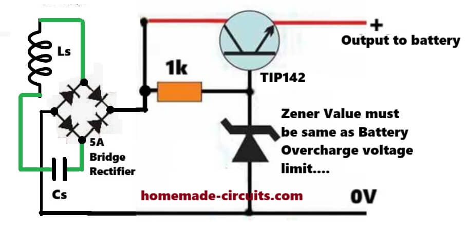
AC to DC Rectifier (Full Bridge)
Now you have high-frequency AC after LC.
Add a bridge rectifier, using fast diodes, UF4007, MUR, or Schottky if voltage is low. Connect LC output to AC inputs of bridge. Bridge + goes to DC+....Bridge – goes to DC–.
At this point the AC becomes pulsating DC, simple conversion.
DC Smoothing Capacitor
After rectifier, connect a large electrolytic capacitor across DC+ and DC–. Also add a small film capacitor, around 0.1 µF, in parallel.
This smooths DC, reduces ripple, protects load a bit. At this point you have unregulated DC, and nothing controlled yet.
Voltage Limiting
Wireless systems can overshoot voltage when load is light or alignment suddenly improves, so voltage can jump fast.
So add this, it is mandatory.
Add Zener plus transistor emitter follower regulator clamp. This limits maximum voltage properly for safe battery charging, and furthermore you can also add an auto cut off circuit for ensuring the battery is never over charged.
Without this, battery or electronics can get damaged.
Current Limiting / Charging Control
Now decide charging method.
For demonstration or DIY work, insert a DC-DC buck converter. Set constant current and battery voltage limit.
This converts wireless DC into safe charging DC. This stage isolates battery behavior from resonance madness, which is important.
Battery Connection
Finally connect battery. Battery + goes to buck output +. Battery – goes to buck output –.
Optionally add reverse polarity diode and a fuse, just for safety.
IMPORTANT NOTES
Receiver resonance must match transmitter. If mismatched, power collapses or heating increases, sometimes both.
Receiver voltage can be VERY high, even at low power. So use high-voltage capacitors and do not connect battery directly.
Alignment sensitivity is real. Closer coils mean higher voltage and higher current. The Rx + SD protection on transmitter saves the design here.